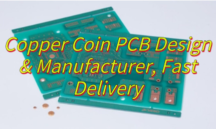
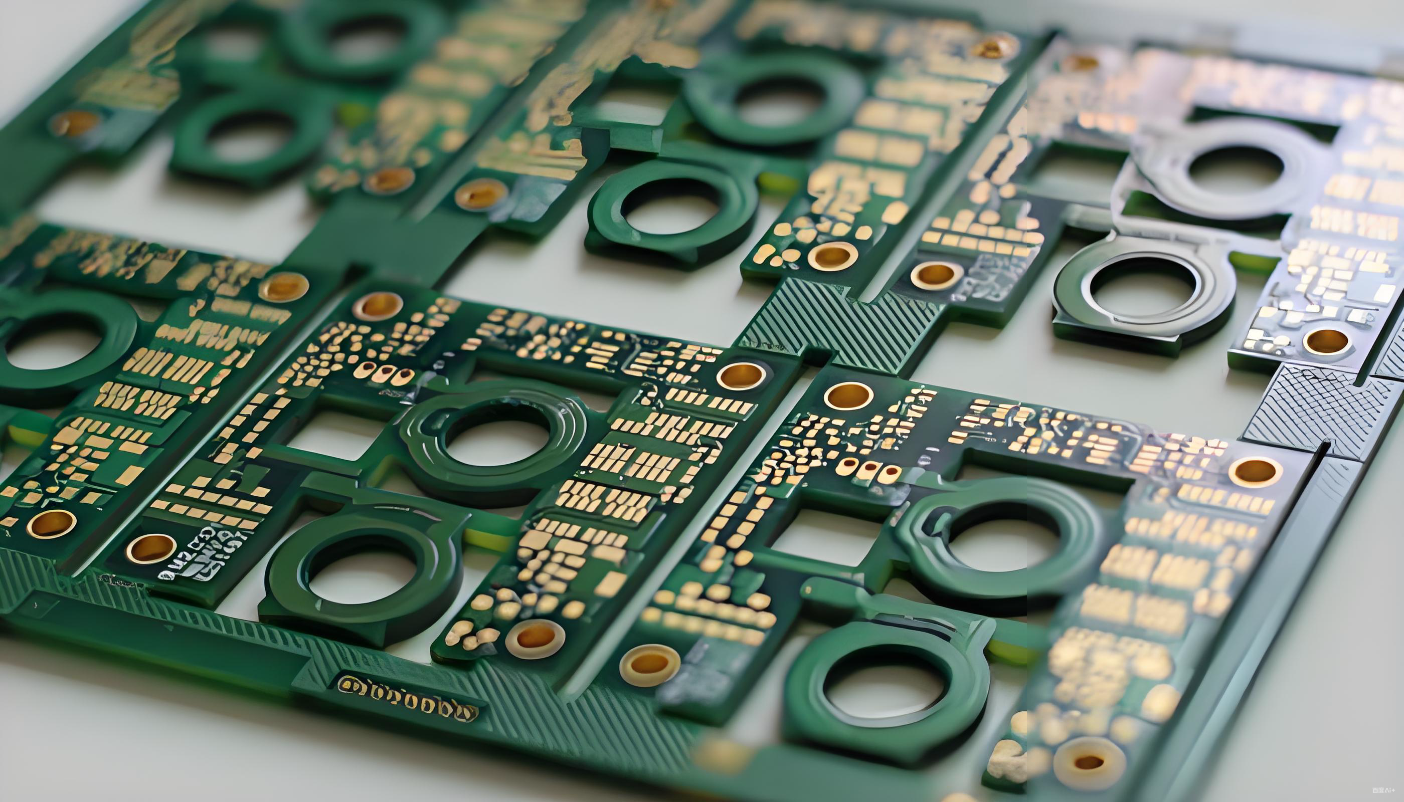
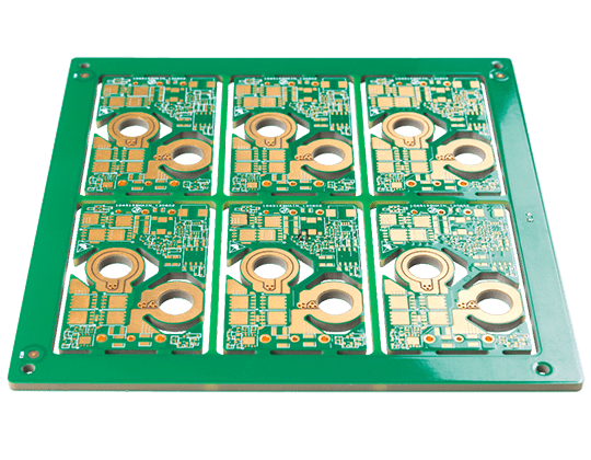
A buried copper coin PCB manufacturer helps engineers create a short, solid-metal heat path through a multilayer circuit board. Instead of forcing concentrated heat through FR-4 and a field of small thermal vias, the design places a machined copper insert directly below or near the hot component. The result is localized thermal management without converting the entire assembly to a metal-core construction.
Buried copper coin technology is especially useful when a compact product combines high heat density with multilayer routing, controlled impedance, HDI features, or a backside heatsink interface. EBest Circuit (Best Technology) manufactures custom PCB and PCBA projects and can review whether a buried, embedded, or press-fit copper structure matches the intended board construction. Contact sales@bestpcbs.com to discuss your layer stack, hot component, copper coin geometry, quantity, and assembly requirements.
What Is a Buried Copper Coin PCB?
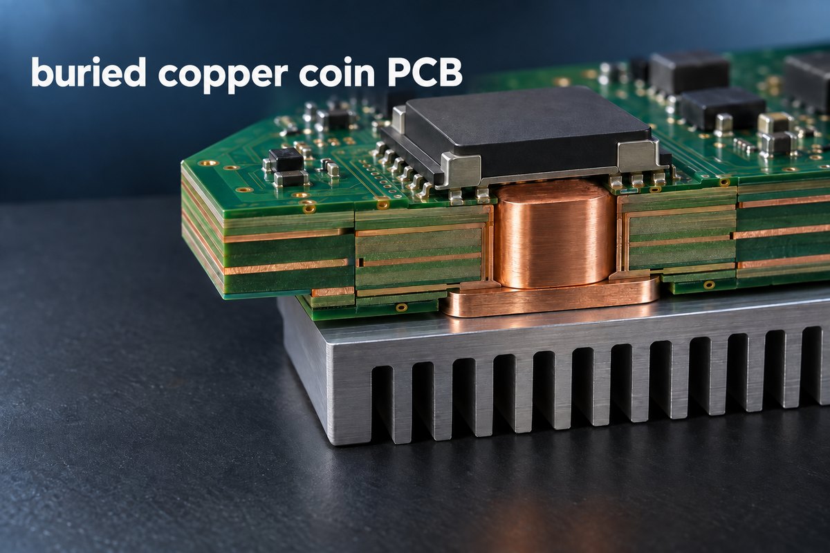
A buried copper coin PCB contains a solid copper insert inside the PCB stackup, normally below a component or thermal pad that produces concentrated heat. Three details define the structure:
- Position: The coin may sit completely inside the multilayer build or extend toward one or both outer surfaces.
- Layer connection: It may connect an outer layer to an internal copper plane, join selected internal layers, or remain electrically isolated and serve only as a thermal path.
- Shape: “Coin” does not mean round. Common forms include rectangular, square, T-shaped, stepped, and custom-machined inserts.
The geometry follows the heat-source area, available routing space, intended layer connection, and mechanical interface on the other side of the PCB.
Manufacturers do not always use “buried,” “embedded,” and “press-fit” in exactly the same way. A cross-sectional drawing is therefore more useful than the name alone because it shows whether the coin is fully enclosed, exposed at one surface, exposed at both surfaces, or inserted into a finished cavity.
How the Buried Copper Coin Transfers Heat
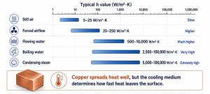
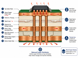
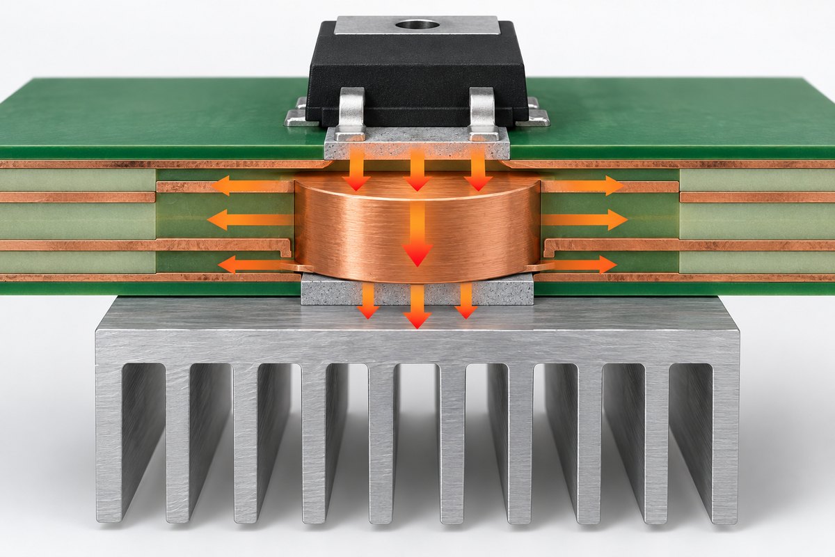
Heat follows every available path away from a component. In an ordinary multilayer PCB, heat may travel laterally through the surface copper, downward through thermal vias, and then into inner planes, a backside copper area, or a heatsink. This approach works well for many components, but the path contains interfaces and materials with much lower thermal conductivity than solid copper.
A copper coin replaces part of that path with a continuous copper body. When the component pad, copper coin, thermal interface material, and heatsink are aligned, heat can move through a much larger solid-metal cross-section. The coin can also spread heat into connected copper planes before it reaches the opposite side of the board.
The improvement does not come from copper alone. It comes from the complete path:
- The component must transfer heat efficiently into the top surface or connected copper layer.
- The coin must have enough contact area at the heat source.
- Intended copper layers must connect to the coin without narrow thermal bottlenecks.
- The opposite side must transfer heat into a chassis, cold plate, heatsink, or other cooling structure.
- Thermal interface material and mounting pressure must support the intended contact.
For this reason, a large coin does not automatically guarantee a low component temperature. Junction-to-case resistance, solder coverage, contact flatness, interface material, airflow, and heatsink capacity remain part of the thermal system. The PCB coin solves the board-level section of the heat path; it does not replace complete thermal analysis and product testing.
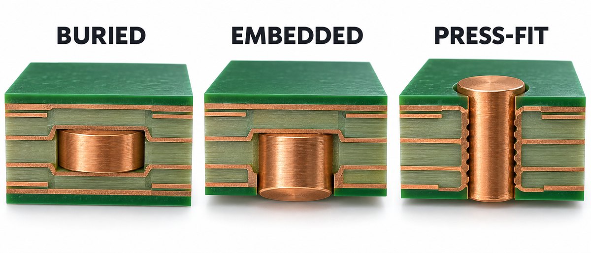
Buried, Embedded, and Press-Fit Copper Coin Structures
Copper coin constructions are commonly grouped by when the insert is added and how it sits inside the board.
Buried copper coin: The insert is incorporated within the multilayer build and does not necessarily pass through the complete board thickness. It can connect selected layers while leaving routing space above or below it. This structure is useful when the thermal path must begin at an internal or subsurface layer, or when an outer layer needs to remain available for routing or component features.
Embedded copper coin: The coin is built into the PCB during multilayer fabrication and may be exposed at one or both surfaces. It can form a mounting or thermal contact surface while remaining integrated with the surrounding laminate. Some suppliers also use “embedded” as the general category that includes buried coins.
Press-fit copper coin: A machined copper part is inserted into a prepared PCB opening with controlled interference. This construction can create a direct path through the board without embedding the coin during lamination. Hole geometry, coin tolerance, insertion force, retention, and surface height all influence the finished result.
Conductive adhesive can also be used for certain copper inserts, depending on the structure and factory capability. Each method changes the mechanical interface, achievable layer connections, thermal contact, manufacturing sequence, and cost. The construction drawing should identify the actual cross-section rather than relying only on one of these category names.
Copper Coin Shapes and Layer Connections
The coin shape determines how heat moves between the component, PCB layers, and external cooling surface.
- Straight rectangular coin: Creates a simple vertical path when the hot pad and backside cooling area have similar dimensions. The upper and lower contact areas remain aligned.
- T-shaped coin: Connects two differently sized interfaces. A narrow upper section can fit beneath a small component pad, while a wider lower section spreads heat toward a larger heatsink or housing contact area. The orientation can also be reversed.
- Stepped coin: Stops at a selected depth or creates different contact areas at different layers. It can connect two internal planes without reaching the component side, or connect a top pad to an inner power plane while leaving lower layers available for routing.
- Connected or isolated coin: Selected layers may connect directly, through plating, or through defined copper features around the insert. Other layers use clearance to remain electrically isolated.
- Thermal-only or electrical-and-thermal coin: The insert can transfer heat only, or it can also carry current or connect to ground. An electrical function must be reflected in the schematic, netlist, clearance, and test plan.
A wider coin generally provides more contact area and heat spreading but occupies more routing space and may interrupt internal planes. A smaller coin preserves board area but reduces the available heat-flow cross-section. The final shape must balance the thermal interface with routing, stackup, component placement, and mechanical packaging.
Buried Copper Coin PCB Manufacturing Process
The exact sequence depends on whether the coin is buried during lamination, embedded with an exposed surface, bonded, or press-fitted after the PCB structure is formed. A typical buried or embedded process follows five main stages:
- Machine the copper coin. The insert is produced to the specified shape and thickness. Its surface may also be prepared for resin bonding, plating, or a defined copper connection.
- Create the matching PCB cavity. The relevant core, prepreg, or subassembly is machined so the coin can occupy its intended position in the stackup.
- Position and laminate the structure. The coin is placed during layup, and the multilayer panel is pressed under a controlled cycle. Prepreg resin flows around the insert and fills the intended interface.
- Establish the finished surface. After lamination, planarization or controlled machining may be used to achieve the specified exposed area and surface height.
- Complete PCB fabrication. The panel continues through the applicable drilling, plating, imaging, etching, solder-mask, surface-finish, routing, and inspection operations.
The copper insert and laminate respond differently to heat and pressure, so cavity geometry, resin volume, stack symmetry, and coin restraint influence the laminated result. If the coin forms a solderable pad, its finished surface must match the assembly design. If it contacts a heatsink or chassis, its usable contact area and height must suit that interface.
For a press-fit construction, the PCB opening and copper part are manufactured separately and then joined by controlled insertion. This avoids embedding the coin during lamination but makes opening dimensions, insertion force, retention, and surface height important. In either approach, the product is a combined PCB, copper-part, and assembly structure—not a standard PCB with an unrelated metal piece added later.
Where Buried Copper Coin PCBs Are Used
Buried copper coin PCBs are used where a small number of components create concentrated heat and the product still requires the routing density or layer count of a conventional multilayer board.
RF and telecommunications equipment: Power amplifiers, radio units, base-station electronics, and other RF assemblies may place a copper coin beneath a high-power device while preserving controlled-impedance routing around it.
Power conversion: DC-DC converters, power supplies, inverters, charging equipment, and power-distribution modules can use copper coins beneath switching devices, power packages, or localized high-current areas.
Industrial and motor-control electronics: Servo drives, motor controllers, robotics controllers, and compact industrial modules may need a direct path from a hot device to a chassis or cold plate.
High-output LED systems: Dense LED modules and illumination controllers can use a copper insert where one device or cluster produces a localized hot spot that exceeds the capability of ordinary vias and surface copper.
Automotive and transportation electronics: Compact power and communication modules may combine high heat density, vibration, restricted airflow, and a housing-based cooling path. The complete construction must still be validated for the applicable operating environment.
Aerospace and defense electronics: Space-constrained RF and power assemblies may use localized solid-copper heat paths when weight, routing density, mechanical design, and reliability requirements justify the additional PCB complexity.
Copper coins are less attractive when heat is spread uniformly across the entire board, when ordinary thermal vias already meet the temperature target, or when the product lacks a useful destination for the extracted heat. In those situations, thicker copper, a metal-core PCB, a larger heatsink, improved airflow, or a different component layout may be more economical.
Buried Copper Coin PCB vs. Thermal Vias and Metal-Core PCBs
Thermal vias, copper coins, and metal-core PCBs solve different thermal layouts.
Thermal vias are easy to include beneath many exposed-pad components and fit normal multilayer manufacturing. They transfer heat through multiple plated barrels into internal or backside copper. They are generally the first option when the heat load and available pad area are compatible with a via array.
A buried copper coin concentrates a larger solid-copper cross-section at one hot location. It is useful when a via field would occupy too much pad area, provide insufficient through-thickness conduction, or interfere with the required package and stackup. It also allows the rest of the PCB to remain a conventional multilayer or HDI construction.
A metal-core PCB uses an aluminum or copper base to spread heat across a much larger portion of the board. It is well suited to many LED, power, and high-temperature assemblies, but the dielectric between the circuit copper and metal base remains part of the thermal path. Multilayer routing and plated-through interconnection can also be more constrained than on a conventional FR-4 multilayer board.
The choice is therefore not simply “which material conducts heat best?” Thermal vias favor simplicity and cost; copper coins favor intense localized heat transfer in a complex multilayer board; metal-core PCBs favor broader heat spreading across the assembly. Some products combine these methods with heavy copper, thermal interface materials, heatsinks, cold plates, or enclosure cooling.
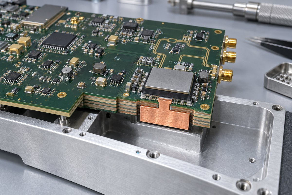
A Practical Buried Copper Coin PCB Example
Consider an eight-layer RF control board with a power amplifier near one edge.
- Board requirements: The amplifier connects to controlled-impedance RF traces on the top layer, while digital control and power routing occupy several inner layers. A machined aluminum housing below the PCB is the main cooling surface.
- Why not a metal-core PCB: A full metal base would complicate the multilayer routing and interconnection required by the RF and control circuits.
- Why not thermal vias alone: A large via field would consume much of the exposed-pad area and still rely on multiple plated barrels for vertical heat transfer.
- Selected structure: One T-shaped copper coin sits beneath the amplifier. Its narrow upper section matches the component’s thermal land, while its wider lower section increases contact area toward the housing.
- Layer and housing connection: Selected ground layers connect to the coin for lateral heat spreading, while signal layers clear the copper body. A thin thermal interface material connects the finished coin surface to the housing after assembly.
The value of this structure is not simply “more copper.” The T-shape connects a small heat source to a larger cooling surface without sacrificing the multilayer routing required by the circuit.
This example is illustrative rather than universal. Actual coin size, surface height, layer connections, finish, interface material, and cooling performance must follow the component power, package data, thermal simulation, housing design, and prototype results.
Why Choose EBest Circuit for Buried Copper Coin PCB Manufacturing?
A buried copper coin PCB requires the copper insert, PCB cavity, multilayer stackup, layer connections, surface height, and assembly interface to work together. EBest Circuit (Best Technology) supports these projects with coordinated engineering, PCB fabrication, component sourcing, and PCBA services.
- One coordinator backed by three engineers: Each project is supported by one business coordinator and three engineers, helping customer questions move quickly between PCB, PCBA, component, and process teams.
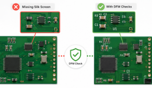
- DFM review by experienced engineers: Engineers with up to 20 years of PCB, PCBA, and product-development experience can review the copper coin structure, cavity, stackup, connected and isolated layers, surface finish, and assembly interface. Customers can receive a DFM review and applicable process recommendations before production.
- Integrated PCB and PCBA services: EBest Circuit combines PCB manufacturing, component sourcing, PCBA assembly, and testing, reducing the need to coordinate the copper coin PCB and subsequent assembly with separate suppliers.
- Prototype and low-volume support: Prototype and low-volume production can support engineering verification before the design moves to a larger production quantity.
- Factory and quality-system support: EBest Circuit operates PCB and PCBA manufacturing facilities under quality systems including ISO 9001, ISO 13485, IATF 16949, and AS9100D.
With 20 years of PCBA experience, EBest Circuit has served more than 10,000 engineers and over 1,800 customers. If you are developing an RF amplifier board, power converter, motor controller, LED system, or another high-heat-density product, send your PCB data, stackup, and copper coin drawing to sales@bestpcbs.com. The team will review the manufacturing requirements and prepare a project-specific quotation.
FAQs About Buried Copper Coin PCB
Is a buried copper coin always completely enclosed inside the PCB?
Not necessarily. Terminology varies among manufacturers. Some buried coins are fully enclosed, while others stop at or become exposed on a selected surface. The cross-section and stackup should define the actual structure.
Can a copper coin carry electrical current as well as heat?
Yes, when it is intentionally connected to a circuit net or ground structure. In that case, current capacity, layer connections, clearances, netlist data, and electrical testing must be considered together with thermal performance.
Is a copper coin better than a thermal-via array?
It can provide a more direct solid-copper path for a concentrated heat source, but it is more complex and costly to manufacture. Thermal vias remain suitable for many components. The correct choice depends on heat density, package geometry, routing, stackup, cooling interface, and cost target.
Can buried copper coins be used in HDI or rigid-flex PCBs?
They can be combined with some high-layer-count, HDI, and rigid-flex constructions, but the feasible structure depends on the individual factory, stackup, cavity, via arrangement, flex location, and lamination sequence. The complete build should be reviewed before release.
What information is most important for a copper coin quotation?
The most useful starting information is the PCB data, stackup, coin cross-section and dimensions, intended layer connections, component and heatsink interfaces, material and finish, quantity, and target application. These details allow the manufacturer to identify the appropriate production route and confirm project-specific capability.
Planning a buried copper coin PCB? Send your PCB files, stackup, copper coin drawing, intended layer connections, quantity, and assembly requirements to sales@bestpcbs.com. EBest Circuit will review the manufacturing requirements and prepare a project-specific quotation.