Largest printed circuit board manufacturers in China are PCB companies with strong production scale, advanced process capability, stable quality systems, and broad customer coverage. This article explains how large PCB manufacturers are ranked, lists 10 major PCB companies in China, and shows how buyers can choose between large-volume PCB makers and custom PCB manufacturers.
Why do buyers search for the largest printed circuit board manufacturers before sending an RFQ?
- They do not know which PCB company is truly reliable.
- They worry that small suppliers cannot handle complex PCB requirements.
- They see many “top PCB manufacturers” lists but no clear comparison logic.
- They are unsure whether a large PCB factory accepts prototype or custom projects.
- They need proof: certifications, capacity, PCB types, PCBA support, and overseas service.
A better supplier selection process should connect company size with real project fit.
- Check ranking factors, not only company names.
- Compare PCB types, process limits, certifications, and lead time.
- Decide whether the project needs high-volume production or flexible customization.
- Review PCBA, component sourcing, and testing capability when needed.
- Choose a PCB manufacturer that matches the product stage and technical risk.
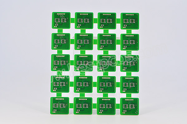
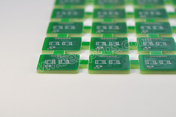
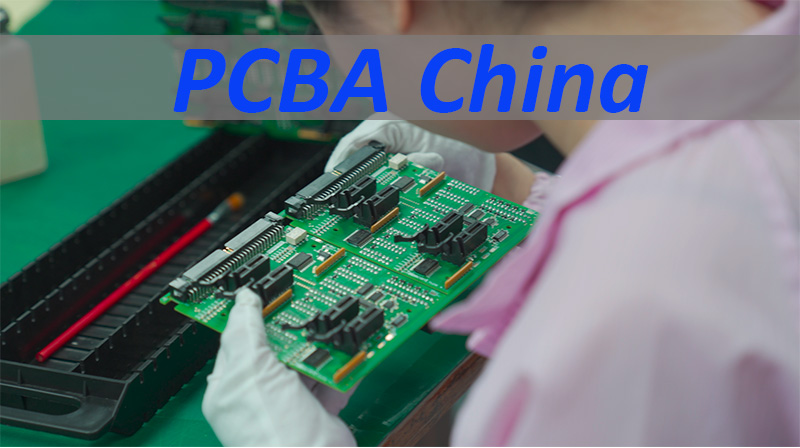
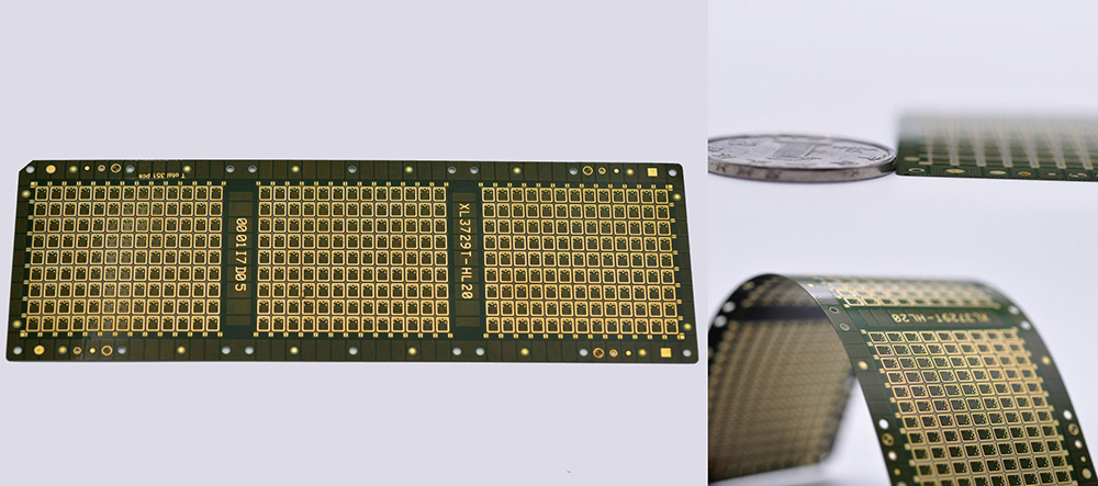
EBest Circuit (Best Technology) is a China-based PCB and PCBA manufacturer supporting custom PCB fabrication, PCB prototype, mass production, component sourcing, PCB assembly, and turnkey PCB solutions. Our capabilities cover FR4 PCB, Metal Core PCB, Ceramic PCB, HDI PCB, flexible PCB, rigid-flex PCB, high-frequency PCB, heavy copper PCB, and PCBA. For project review or quotation, contact sales@bestpcbs.com.
What Does “Largest Printed Circuit Board Manufacturers” Mean?
The largest printed circuit board manufacturers are usually judged by revenue, production capacity, customer base, factory scale, technical capability, and global supply coverage. However, “largest” does not always mean “best for every project.”
A company may be very large because it serves smartphone, server, automotive, telecom, or AI hardware programs. That does not automatically mean it is the best choice for a small-batch ceramic PCB, an urgent prototype, or a custom PCBA order.
| Ranking Factor | Why It Matters |
|---|---|
| Revenue | Market scale |
| Capacity | Volume support |
| PCB Types | Technical range |
| Certifications | Quality proof |
| Customers | Industry trust |
| Overseas Support | Export readiness |
The global PCB market is large and still growing. ResearchAndMarkets estimated the PCB market at $67.9 billion in 2023 and projected it to reach $92.4 billion by 2029, which explains why buyers pay close attention to major PCB manufacturing regions and large suppliers.
For buyers, the practical meaning is simple: use “largest” as a starting point, not the final decision.
How Are the Largest PCB Manufacturers in China Ranked?
The largest PCB manufacturers in China can be ranked in different ways. Some lists focus on revenue. Others focus on output, factory area, domestic ranking, global ranking, or a specific product category such as HDI PCB, FPC, IC substrate, server PCB, or automotive PCB.
A clean ranking method should include:
- Business scale: revenue, capacity, and customer base.
- Product capability: multilayer PCB, HDI PCB, FPC, rigid-flex PCB, heavy copper PCB, high-frequency PCB.
- Quality system: ISO, IATF, AS9100, UL, RoHS, REACH, or medical-related systems.
- Industry coverage: automotive, communication, data center, medical, industrial, consumer electronics.
- Engineering support: DFM, stack-up review, impedance control, PCBA, testing, and overseas service.
This is why PCB manufacturer ranking should not be read like a simple winner list. A high-volume factory may be excellent for server boards but less flexible for small custom projects. A custom PCB manufacturer may not be the largest, but it may provide better engineering response, MOQ flexibility, and special-board support.
Top 10 Largest Printed Circuit Board Manufacturers in China
The following list is a practical B2B reference of large and well-known printed circuit board manufacturers in China. The order may vary by year, revenue source, and ranking method, so buyers should use it as a supplier research starting point rather than a fixed audited ranking.
| Company | Strong Area | Best Fit |
|---|---|---|
| Shennan Circuits | PCB + IC substrate | High-reliability electronics |
| Dongshan Precision / Multek | PCB, FPC, rigid-flex | High-density projects |
| Victory Giant Technology | AI server PCB | High-speed, high-volume |
| Kinwong | Multilayer PCB | Global PCB supply |
| WUS Printed Circuit | Server, AI, automotive | HPC and data center |
| Suntak Technology | Multilayer, HDI | Large-volume PCB |
| Aoshikang Technology | High-precision PCB | Server, auto, telecom |
| Fastprint Circuit Tech | Prototype, small batch | Engineering projects |
| Founder PCB | Multilayer, HDI | Communication, smart devices |
| Guangdong Ellington | Double-sided, multilayer | High-density PCB |
- Shennan Circuits: Its core business covers printed circuit boards, packaging substrates, and electronic assembly, making it one of China’s more technology-driven PCB companies.
- Dongshan Precision / Multek: Multek supports rigid PCB, FPC/FPCA, PCB, and rigid-flex products. Its rigid PCB capability includes high-layer-count and HDI structures.
- Victory Giant Technology: Victory Giant is recognized as a major Chinese PCB manufacturer and is strongly associated with AI server and high-performance computing PCB demand.
- Kinwong: Kinwong reported 2024 annual revenue of $1.762 billion and describes itself as one of the world’s largest printed circuit board suppliers.
- WUS Printed Circuit: WUS manufactures PCBs for high-speed servers, accelerator modules, automotive domain controllers, AI, HPC, autonomous driving, medical, industrial, and navigation applications.
- Suntak Technology: Suntak reports large annual capacity and positions itself as a listed high-tech company producing circuit boards for communications, servers, computers, medical electronics, industrial HDI, automotive electronics, mobile phones, and optoelectronics.
- Aoshikang Technology: Aoshikang focuses on R&D, production, and sales of high-precision PCBs used in data centers, servers, automotive electronics, communications, and consumer electronics.
- Fastprint Circuit Tech: Fastprint is headquartered in Shenzhen, listed on the Shenzhen Stock Exchange, and operates manufacturing campuses in Guangzhou, Yixing, and the UK.
- Founder PCB: Founder PCB is a PCB company headquartered in Zhuhai, Guangdong, with a long operating history in multilayer and HDI PCB manufacturing.
- Guangdong Ellington: Guangdong Ellington focuses on high-precision, high-density double-sided and multilayer printed circuit boards.
Why Are Many of the Largest PCB Manufacturers Based in China?
Many of the largest PCB manufacturers are based in China because China has a complete electronics manufacturing ecosystem. PCB production depends on copper foil, laminate, drilling, plating, imaging, solder mask, surface finish, SMT, components, testing, packaging, and export logistics. China has dense supply-chain support for each step.
China’s PCB manufacturing advantage usually comes from:
- Strong electronics supply chains in the Pearl River Delta and Yangtze River Delta.
- Large demand from communication, automotive, consumer electronics, AI servers, and industrial equipment.
- Mature support for PCB materials, surface treatment, mechanical processing, and assembly.
- Wide factory choices, from high-volume PCB manufacturers to custom PCB manufacturers.
- Strong export experience for overseas electronics companies.
For buyers, this means China is not only a low-cost PCB sourcing region. It is also a technical manufacturing hub with large printed circuit board manufacturers, prototype PCB manufacturers, PCBA service providers, and special PCB factories.
Large PCB Manufacturers vs Custom PCB Manufacturers in China
Large PCB manufacturers and custom PCB manufacturers serve different needs. The largest printed circuit board manufacturers in China are often strong in scale, automation, large customers, and stable high-volume production. Custom PCB manufacturers are often more flexible in special boards, engineering support, prototype orders, and communication.
| Supplier Type | Best For | Possible Limitation |
|---|---|---|
| Large PCB manufacturers | High-volume production | Less flexible MOQ |
| Custom PCB manufacturers | Special PCB projects | Smaller scale |
| Prototype PCB manufacturers | Fast engineering samples | Limited mass volume |
| PCBA manufacturers | Finished assemblies | Needs BOM clarity |
A large factory is a good choice when the project has stable design files, large demand, and clear process requirements. A custom printed circuit board manufacturer is often better when the project needs HDI PCB, ceramic PCB, Metal Core PCB, heavy copper PCB, rigid-flex PCB, impedance control, unusual thickness, special materials, or PCBA support.
The right question is not “Which PCB manufacturer is the largest?” The better question is: “Which manufacturer fits this product?”
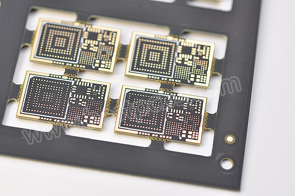
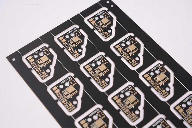
What PCB Types Do Top Printed Circuit Board Manufacturers in China Produce?
Top printed circuit board manufacturers in China usually produce a wide range of PCB types. The exact capability depends on each factory’s equipment, process control, materials, certifications, and target markets.
| PCB Type | Typical Application |
|---|---|
| FR4 PCB | General electronics |
| Multilayer PCB | Industrial, telecom |
| HDI PCB | Compact devices |
| Flexible PCB | Wearables, modules |
| Rigid-Flex PCB | Space-limited products |
| Metal Core PCB | LED, power modules |
| Ceramic PCB | High heat, power |
| Heavy Copper PCB | High-current systems |
| High-Frequency PCB | RF, communication |
| PCBA | Finished assemblies |
Large China PCB manufacturers often focus on high-volume multilayer boards, HDI boards, server boards, automotive boards, or consumer electronics. Custom PCB manufacturers may support more specialized structures, smaller quantities, or faster engineering feedback.
For buyers, PCB type is a key filter. A supplier strong in mobile-phone HDI may not be the best option for ceramic PCB. A factory strong in heavy copper may not be ideal for fine-pitch rigid-flex. The PCB type should guide supplier selection before price comparison begins.
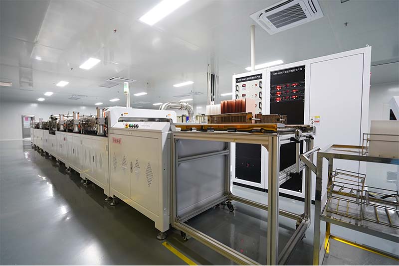
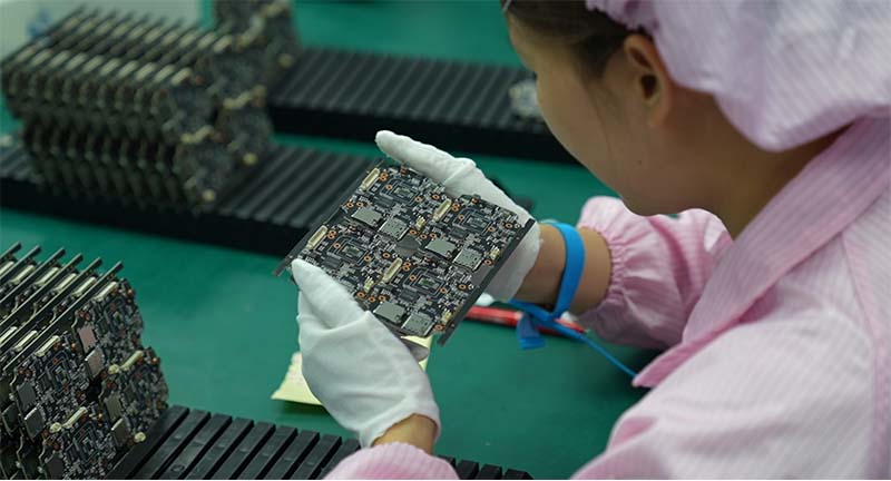
How EBest Circuit Supports Custom PCB and PCBA Manufacturing
EBest Circuit (Best Technology) is not positioned only as one of the largest printed circuit board manufacturers by revenue. Its value is stronger for customers who need custom PCB fabrication, special PCB technologies, PCB prototype, mass production, component sourcing, PCB assembly, and turnkey support.
| EBest Circuit Capability | Proof Point |
|---|---|
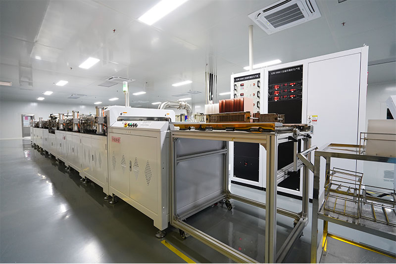
| Industry Experience | 20+ years |
| PCB Capacity | 260,000 sq ft/month |
| Board Variety | 1,000+ types/month |
| Countries Served | 40+ |
| Delivery Record | 97% on-time delivery |
| Certifications | ISO, IATF, AS9100D, UL |
EBest Circuit supports FR4 PCB, Metal Core PCB, Ceramic PCB, HDI PCB, flexible PCB, rigid-flex PCB, high-frequency PCB, heavy copper PCB, PCB prototype, mass production, component sourcing, and PCB assembly. The company also holds ISO 9001:2015, ISO 13485:2016, IATF 16949, AS9100D, UL, REACH, and RoHS certifications.
This makes EBest Circuit suitable for buyers who need more than a commodity PCB supplier. If your project involves custom board structure, thermal design, special materials, PCBA assembly, or overseas communication, EBest Circuit can support the project from PCB review to finished delivery.
How to Compare the Largest PCB Manufacturers in China
When comparing the largest PCB manufacturers in China, do not compare only the company name. Compare the project fit.
Use this simple checklist:
- PCB type: FR4, HDI, FPC, rigid-flex, Metal Core, Ceramic, heavy copper, high-frequency.
- Technical limits: layers, line width/space, hole size, copper thickness, impedance, board thickness.
- Quality proof: ISO, IATF, AS9100D, ISO 13485, UL, RoHS, REACH.
- Order type: prototype, low volume, medium volume, high volume.
- Support scope: PCB only, PCB + PCBA, sourcing, testing, box build.
- Lead time: normal lead time, urgent order support, sample response.
- Communication: English support, engineering feedback, quotation clarity.
The largest PCB manufacturer may be excellent for one program but unsuitable for another. A server PCB project may need high-layer-count and high-speed material capability. A medical device PCB may need ISO 13485-related quality control. A power module may require heavy copper, Metal Core PCB, or Ceramic PCB.
For overseas customers, communication and RFQ clarity are also important. A good supplier should clearly review Gerber files, BOM, stack-up, surface finish, quantity, tolerance, testing needs, and delivery schedule before quoting.
How to Choose the Right PCB Manufacturer Beyond Company Size
Company size is only one part of supplier selection. The right PCB manufacturer should reduce your project risk.
Choose based on these points:
| Buyer Need | What to Check |
|---|---|
| Prototype | Fast review and lead time |
| Mass production | Capacity and yield control |
| Special PCB | Process experience |
| PCBA | Assembly and sourcing |
| Regulated industry | Certifications |
| Overseas order | Export support |
| Urgent project | Delivery record |
If the project is stable, high-volume, and price-sensitive, a large PCB manufacturer may be the best fit. If the project needs special materials, custom stack-up, thermal design, ceramic PCB, heavy copper PCB, or turnkey PCBA, a custom PCB manufacturer may provide better support.
For many B2B buyers, the best PCB partner is not always the biggest company. It is the company that understands the board, the application, the quality requirement, and the production schedule.
FAQs About Largest Printed Circuit Board Manufacturers
What are the largest printed circuit board manufacturers in China?
They are large PCB companies with strong capacity, market presence, technical capability, and customer coverage. Examples include Shennan Circuits, Dongshan Precision/Multek, Victory Giant, Kinwong, WUS, Suntak, Aoshikang, Fastprint, Founder PCB, and Guangdong Ellington.
Are the largest PCB manufacturers always the best choice?
Not always. Large PCB manufacturers are strong in scale, but custom PCB manufacturers may be better for special materials, prototype projects, small batches, or PCB assembly support.
How are PCB manufacturers ranked?
PCB manufacturers may be ranked by revenue, output, production capacity, product type, technology level, customer base, certifications, or market influence.
What PCB types do China printed circuit board manufacturers produce?
Common PCB types include FR4 PCB, multi-layer PCB, HDI PCB, flexible PCB, rigid-flex PCB, Metal Core PCB, Ceramic PCB, high-frequency PCB, heavy copper PCB, and PCBA.
Why are many top PCB manufacturers in China?
China has a complete electronics supply chain, large production capacity, mature PCB processes, strong component and assembly support, and extensive export experience.
What should I prepare before asking for a PCB quote?
Prepare Gerber files, stack-up, material requirement, copper thickness, board thickness, surface finish, quantity, tolerance, testing requirement, and delivery target.
Can EBest Circuit support both PCB and PCBA?
Yes. EBest Circuit supports custom PCB fabrication, component sourcing, PCB assembly, inspection, testing, prototype, and mass production.
How do I choose between a large PCB manufacturer and a custom PCB manufacturer?
Choose based on PCB type, order quantity, technical risk, certifications, lead time, MOQ, assembly needs, and communication quality.
In conclusion, largest printed circuit board manufacturers in China are important reference points for buyers who want to understand supplier scale, technical capability, and PCB manufacturing strength. This article explained how large PCB manufacturers are ranked, listed 10 major PCB companies in China, reviewed common PCB types, and showed how buyers can choose beyond company size.
EBest Circuit (Best Technology) supports customers who need custom PCB fabrication, special PCB technologies, PCB prototype, mass production, component sourcing, PCB assembly, and turnkey support. With 20+ years of experience, 260,000 sq ft monthly PCB capacity, 1,000+ board types per month, 40+ countries served, 97% on-time delivery, and certifications including ISO 9001, ISO 13485, IATF 16949, AS9100D, UL, REACH, and RoHS, EBest Circuit is a practical partner for custom PCB and PCBA projects. For PCB quotation or project review, send your Gerber files, PCB specifications, quantity, and assembly requirements to sales@bestpcbs.com.