





Differential pair PCB design works when two coupled traces carry opposite-polarity signals through a controlled geometry and an uninterrupted return environment. Good results depend on the complete channel, not on matching two visible trace lengths or copying a width-and-gap rule from another stackup.
Translate the interface requirement into impedance geometry, route the pair without avoidable discontinuities, set a defensible length-matching limit, and release enough data for fabrication and verification. For an early manufacturability check on a real layout, send the stackup, target impedance, Gerber or ODB++ data, and relevant interface requirements to sales@bestpcbs.com for a free DFM review.

What Is a Differential Pair in PCB Design?
A differential pair is a matched signal path in which the receiver responds mainly to the voltage difference between two conductors. The two traces are usually named positive and negative, but the essential behavior is the equal-and-opposite signal relationship, not the labels. The pair should be treated as one transmission structure from transmitter pins through vias, connectors, and PCB routing to the receiver pins.
In differential pair PCB design, coupling between the two traces can help the receiver reject noise that appears similarly on both conductors. That benefit is conditional. Unequal geometry, different reference-plane exposure, asymmetric vias, stubs, or unequal loading can convert part of the differential energy into common-mode energy. A visually neat pair can therefore perform poorly if its electrical environment is not symmetric.
The controlled properties are the pair’s target differential impedance, trace geometry, reference plane, transition structure, allowed discontinuities, and skew budget. Their limits come from the interface specification and system timing analysis, then become stackup, layout, and fabrication controls.
How Do Differential Pairs Improve Signal Integrity in High-Speed PCBs?
Differential signaling improves noise tolerance when both traces experience closely matched electrical conditions. A receiver subtracts one input from the other, so noise coupled equally into both traces is partly rejected. The opposite currents also produce fields that can partially cancel at a distance, which can reduce radiated coupling compared with a poorly controlled single-ended route.
The benefit is not automatic for a high-speed PCB differential pair. Common-mode rejection deteriorates when one trace crosses a plane split, sees a different via field, passes closer to a noisy aggressor, or accumulates substantially different delay. Mode conversion can then increase emissions, receiver jitter, and eye closure even if continuity and nominal impedance appear acceptable.
Evaluate signal integrity across the full channel because the launch, connector, package, vias, routing, terminations, and receiver all contribute. Apply the same return-path and transmission-line checks described for controlled signal transmission PCB design.
How Is Differential Pair PCB Impedance Calculated from the Stackup?
Differential impedance is calculated from the pair geometry, conductor properties, and surrounding dielectric structure. It is not determined by trace width alone. The calculation must use the actual routing layer and the intended fabricated stackup, including the reference-plane relationship.
The following inputs are the minimum useful basis for a differential pair impedance calculation:
- Trace geometry: define finished conductor width, pair spacing, copper thickness, and whether the traces are external microstrip or internal stripline.
- Dielectric geometry: define the finished distance from the signal layer to each relevant reference plane, not merely the prepreg or core catalog thickness before processing.
- Material model: use a design dielectric constant and loss model appropriate to the laminate, frequency range, and solver method rather than treating one catalog Dk value as universal.
- Fabrication effects: account for etching, trapezoidal conductor shape, copper plating where applicable, resin flow, and solder mask on external layers when these effects are material to the target.
| Input | Electrical effect | Release or verification action |
| Trace width | Changes each conductor’s single-ended impedance and its interaction with the partner trace | State whether the value is design width or expected finished width |
| Pair spacing | Changes mutual coupling and therefore differential impedance | Define edge-to-edge or center-to-center convention explicitly |
| Plane distance | Changes field concentration and impedance sensitivity | Confirm the finished dielectric thickness with the fabricator |
| Dielectric properties | Affect impedance, delay, and loss | Identify the approved material family and design-property basis |
| Copper profile and thickness | Affect effective geometry and conductor loss | Include finished copper requirements and relevant foil constraints |
A solver result is therefore conditional on its inputs. If the fabricator adjusts width to meet impedance, the released drawing should make that permission explicit and retain a controlled record of the approved stackup and resulting geometry.
The impedance calculation record should identify the solver assumptions, differential target, and exact stackup revision. This prevents a valid result from being reused after a material or layer-geometry change makes it obsolete.
How Should You Use a PCB Differential Pair Impedance Calculator?
Use a PCB differential pair impedance calculator for early geometry exploration, then confirm the production geometry with the fabricator’s stackup and field-solver method. Different calculators can disagree because they use different closed-form equations, conductor models, dielectric assumptions, and solder-mask treatment.
- Lock the interface requirement: obtain the target impedance and any permitted tolerance from the applicable interface specification or system requirement; do not choose a familiar value by habit.
- Enter one real stackup: use the intended routing layer, reference planes, finished dielectric distances, copper thickness, design Dk basis, width, and edge-to-edge spacing.
- Run sensitivity checks: vary width, spacing, dielectric thickness, and material properties within realistic fabrication ranges to identify which input dominates the result.
- Compare methods carefully: if two tools disagree, compare their input definitions and models before averaging their outputs; the disagreement is evidence that the assumptions need review.
- Close the fabrication loop: submit the target and preliminary geometry for stackup confirmation, then update the layout and controlled-impedance drawing to match the approved production construction.
An online calculator is most useful as a screening tool. A 2D field solver or fabricator impedance model better represents multilayer geometry and manufacturing effects, but even that result must remain tied to the same material and stackup revision used for production.
How Do You Select Differential Pair Trace Width and Spacing?
Select differential pair trace width and spacing together because both affect impedance, coupling, loss, routing density, and manufacturability. There is no universally correct width-to-gap ratio. A geometry that works on one layer may miss the target after a stackup, copper, or material change.
Width is often constrained by loss, current density, breakout space, and fabrication capability. Differential pair spacing controls mutual coupling but also affects how strongly the pair depends on its partner compared with the reference plane. Very tight spacing can make etch variation more influential and may complicate neck-down areas; wide spacing reduces pair coupling and increases the need for consistent reference-plane behavior.
- Start with the stackup: choose the routing layer and reference plane before optimizing width and spacing.
- Prioritize the target: solve for the required impedance while preserving manufacturable geometry and acceptable channel loss.
- Control transitions: define how far neck-down may extend near pads, vias, or connectors and include those regions in channel review.
- Check process sensitivity: select geometry that remains acceptable across realistic finished-width and dielectric-thickness variation.
Treat differential pair spacing as a stackup-specific design result, not a reusable rule of thumb. Record the final geometry by impedance class and layer so that layout, CAM review, and coupon verification refer to the same definition.
How to Route Differential Pair Traces in PCB?
Route the two conductors as one continuous electrical structure with consistent geometry, reference, and transition symmetry. The route should be planned before dense single-ended signals consume the cleanest corridors.
- Confirm endpoints and constraints: identify the transmitter and receiver pin assignments, polarity, target impedance, routing layer, allowed via structure, and timing budget from controlled design inputs.
- Plan the return environment: choose a path over a continuous reference plane and avoid splits, voids, antipad discontinuities, and reference changes that force return current to detour.
- Route the pair together: maintain the approved width and spacing through the main path, keeping the two traces exposed to similar nearby copper, components, and aggressors.
- Minimize discontinuities: keep stubs short, limit unnecessary vias, and avoid long neck-down regions; each discontinuity should have a clear routing or breakout reason.
- Match transitions: use symmetric via structures and comparable pad, antipad, and escape geometry for both conductors; review connector and package launches as part of the channel.
- Correct local skew near its source: add only the delay required by the interface budget and avoid dense serpentine patterns that introduce extra coupling or impedance disturbance.
- Verify the finished route: run geometry and connectivity checks, inspect reference continuity and coupling context, and use channel simulation when edge rate, loss, or discontinuity severity makes it necessary.
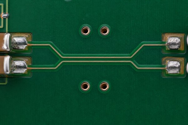
Accept the route only after checking geometry and reference continuity across the complete channel, including breakout and transition regions where the traces cannot remain perfectly parallel.
Which Differential Pair PCB Layout Guidelines Control Vias and Reference Planes?
The most consequential differential pair PCB layout guidelines keep both conductors symmetric through layer transitions and preserve a short return path between reference planes. A via transition changes capacitance, inductance, coupling, and return-current geometry, so it cannot be treated as a neutral connection.
- Use paired transitions: keep signal-via type, barrel length, pad stack, antipad, and stub condition equivalent for the two traces.
- Provide return continuity: when the reference changes between planes, place suitable stitching paths nearby according to the reference-net and stackup design.
- Control via stubs: evaluate unused barrel length against channel bandwidth; backdrilling or alternative via structures are design choices, not universal requirements.
- Avoid plane voids: do not route across splits, cutouts, large antipad fields, or sparse reference copper without analyzing the return-path effect.
- Review coupled neighborhoods: maintain adequate separation from unrelated high-speed routes, clocks, switching nodes, and board edges based on coupling analysis rather than one generic spacing multiple.
For a complex differential pair PCB layout, inspect the launch and transition geometry in 3D or with a suitable electromagnetic model when a simple cross-section solver cannot represent the discontinuity. Judge the transition against the channel requirement rather than its apparent symmetry in a 2D screenshot.
How Much Differential Pair Length Matching Is Actually Required?
Differential pair length matching should be based on allowed intra-pair skew, not on a universal length difference. The permitted mismatch depends on the interface, signal edge rate, receiver tolerance, package skew, connector skew, and the propagation delay of the actual stackup.
Intra-pair matching controls the time difference between the positive and negative conductors of one pair. Inter-pair matching controls timing among separate lanes or pairs. These are different constraints and should not share one rule unless the interface specification explicitly makes them identical.
Convert the electrical skew budget into a physical-length budget using the propagation delay for the routed layer, then subtract known package, connector, and breakout contributions. Correct mismatch close to the location that created it. Long, tightly folded meanders can add self-coupling and local impedance disturbance, so a nominally perfect length report does not guarantee a better channel.
The layout release should identify which nets use intra-pair matching, which groups require inter-pair matching, the source of each limit, and whether the CAD tool measures pad-to-pad routing, pin-to-pin delay, or another defined path. This prevents a tolerance from being applied to the wrong electrical quantity.
What Causes Differential Pair Signal Integrity Failures?
Differential pair signal integrity failures usually arise from discontinuity, asymmetry, excessive loss, crosstalk, or an incorrect constraint source. A diagnosis should connect the observed symptom to a physical mechanism and a measurement or simulation that can distinguish it from other causes.
| Observed symptom | Likely mechanism | Useful verification | Corrective direction |
| Reflection or eye closure near a transition | Via, connector, neck-down, or plane discontinuity | TDR localization and channel simulation | Refine the transition geometry and return path |
| Unexpected emissions or common-mode energy | Pair asymmetry, skew, or unequal reference exposure | Common-mode conversion analysis and near-field probing | Restore symmetry and remove the source of unequal delay |
| Intermittent margin across builds | Geometry or material sensitivity near the limit | Coupon data, cross-section results, and lot correlation | Adjust nominal geometry or tighten the relevant controlled input |
| Crosstalk that changes with activity | Insufficient separation or long parallel exposure to aggressors | Victim-aggressor simulation or oscilloscope correlation | Increase isolation, change layer assignment, or shorten exposure |
| Calculator and production results disagree | Different stackup, Dk, copper, or geometry definitions | Input-by-input model comparison and coupon review | Reconcile the production stackup and finished geometry basis |
When reviewing a failing differential pair PCB, begin with the channel map and locate where geometry, reference, or symmetry changes. This narrows the investigation more effectively than changing multiple routing rules at once.
What Should You Include in a Differential Pair PCB Manufacturing Package?
Release a differential pair PCB as a controlled impedance construction with explicit net classes, stackup assumptions, fabrication authority, and verification requirements. Gerber data alone may show the artwork, but it does not reliably communicate the electrical intent or which dimensions the fabricator may tune.
- Impedance schedule: list each differential impedance class, target, tolerance source, routing layer, and representative net names.
- Stackup definition: identify copper layers, reference planes, finished dielectric thicknesses, approved material family, and the design-property basis used for modeling.
- Geometry convention: state finished or design trace width, edge-to-edge spacing, copper thickness, and any permitted fabricator adjustment.
- Coupon plan: define whether a representative impedance coupon is required, which structures it covers, and what report or data should be returned.
- Verification method: identify the agreed TDR or other measurement approach, reporting format, and project-specific acceptance basis.
- Change control: require review when material, stackup, copper, trace geometry, or impedance-adjustment assumptions differ from the approved construction.
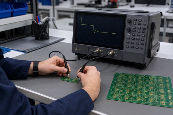
Ask for the production stackup and impedance report to be revision-linked to the order. For high-risk channels, cross-section data and representative coupon results can help separate artwork errors from fabrication variation. These records also make later repeat orders and engineering changes easier to compare.
Frequently Asked Questions About Differential Pair PCB Design
Q1: Is differential impedance always twice the single-ended impedance?
A1: No, coupling changes the relationship. When the traces are electromagnetically coupled, the differential impedance depends on both each trace’s impedance and their mutual interaction. The result approaches a simple two-times relationship only under limited weak-coupling conditions. Use the pair geometry and actual stackup in an appropriate calculator or field solver.
Q2: Should a differential pair remain at the same spacing everywhere?
A2: Keep the approved spacing through the main route, but controlled local exceptions may be necessary. Pads, vias, connectors, and breakout regions can force geometry changes. Minimize their length, keep both sides symmetric, and include electrically significant transitions in simulation or review instead of assuming the main-route impedance represents the entire channel.
Q3: Can differential pairs cross a split in the reference plane?
A3: A plane split is normally a return-path discontinuity and should be avoided. Crossing it can enlarge the current loop, increase radiation, and create mode conversion. If a design constraint makes a reference transition unavoidable, engineer a defined return path and validate the transition rather than routing across an uncontrolled void.
Q4: Does polarity swapping fix a routing problem?
A4: Polarity inversion is interface-dependent and does not repair poor channel geometry. Some receivers support polarity reversal, but that feature must be confirmed in the device or interface documentation. Even when allowed, the two traces still require symmetric transitions, continuous references, controlled impedance, and an acceptable skew budget.
Q5: Should differential pair meanders be placed anywhere there is space?
A5: Place only the required correction near the source of mismatch. Dense or long meanders can couple to themselves, disturb impedance, and add more delay than a simple geometric estimate suggests. Keep adequate spacing between adjacent serpentine segments and verify the result against the electrical skew budget.
Q6: Is a 90-ohm or 100-ohm target suitable for every interface?
A6: No, the target must come from the applicable interface specification. Those values are common examples across different interface families, not interchangeable defaults. Confirm the differential target, tolerance, reference test condition, and whether connector or package effects are included before creating the PCB rule.
Q7: Does equal CAD length guarantee equal electrical delay?
A7: Equal reported length does not guarantee equal delay. The traces can experience different dielectric environments, reference discontinuities, vias, connector paths, or local coupling. For demanding channels, evaluate electrical delay and skew across the complete path rather than relying only on a geometric length column.
Q8: When is backdrilling worth considering?
A8: Consider backdrilling when unused via stubs materially reduce channel margin. The decision depends on data rate, edge content, via length, board thickness, connector topology, and the measured or simulated channel response. It is not required for every differential pair and should be specified with achievable stub and registration limits.
Q9: Why can an impedance coupon pass while the product channel still fails?
A9: A coupon represents selected fabrication geometry, not every product discontinuity. It may confirm the line construction while the product still contains problematic launches, vias, plane voids, connectors, or routing asymmetry. Use coupon data to verify fabrication, then diagnose the full product channel separately.
Q10: What files help a fabricator review a controlled differential pair design?
A10: Provide the artwork and the electrical construction requirements together. Useful inputs include Gerber or ODB++, NC drill data, stackup, impedance schedule, net names, width-and-spacing convention, material requirements, coupon request, and any permission to adjust geometry. Add assembly or connector information when it affects the channel review.
Conclusion
A reliable differential pair begins with an interface-derived electrical requirement and ends with a revision-controlled manufacturing record. Calculate impedance from the real stackup, route both conductors through the same electrical environment, distinguish intra-pair from inter-pair matching, and verify production with the evidence appropriate to the channel risk.
If your design is approaching layout release, send the Gerber or ODB++, stackup, impedance schedule, target interfaces, quantities, and requested verification records to sales@bestpcbs.com. EBest Circuit can review the controlled-impedance fabrication inputs and return project-specific DFM questions and quotation requirements without replacing the interface owner’s final electrical validation.
You may also like




Tags: Differential Pair Impedance, Differential Pair Length Matching, Differential Pair PCB Layout, Differential Pair PCB Routing