Copper skin depth describes how far alternating current penetrates into a conductor at a particular frequency. At high frequency, current density falls with depth instead of remaining uniform through the copper. This means thicker PCB copper can reduce DC resistance without producing the same proportional reduction in RF conductor loss.
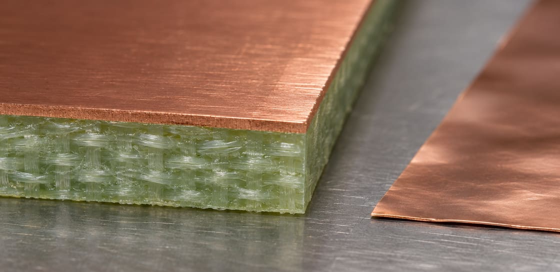
Use this guide when comparing copper thickness or foil for an RF line. It explains the calculation, gives a frequency table and separates skin depth from the other effects that determine the loss of the finished transmission line.
What does one skin depth mean?
In the ideal good-conductor model, current-density amplitude falls to 1/e, about 37% of its surface value, at one skin depth. Current does not stop at a sharp boundary. The field and current distribution continue to decay into the metal.
Skin depth is therefore not a layer of copper that can be peeled away or a fixed property independent of frequency. It is a calculated length for stated material properties and excitation conditions.
Which inputs define the copper calculation?
The model uses frequency, conductivity and permeability. For the following teaching calculations, assume smooth bulk copper with conductivity 5.8 × 10^7 S/m, relative permeability approximately 1, and μ0 approximately 4π × 10^-7 H/m. These are illustrative near-room-temperature model inputs, not guaranteed foil specifications.
Here f is frequency in hertz (Hz), σ is conductivity in siemens per meter (S/m), and μ is permeability in henries per meter (H/m). The calculated skin depth δ and conductor thickness t must use the same length unit when comparing t/δ.
Use δ = √[1 ÷ (π f μ σ)]. Conductivity can change with temperature and material condition. If the application depends on a supplier’s actual foil properties, use those values and retain the model assumptions.
Calculate a frequency table before choosing thickness
For the stated smooth-copper assumptions, the calculated values are approximately:
| Frequency | Skin depth | Interpretation |
| 1 MHz | 66.1 µm | Can exceed thin foil thickness |
| 10 MHz | 20.9 µm | Comparable with some PCB foil |
| 100 MHz | 6.61 µm | Smaller than 35 µm copper |
| 1 GHz | 2.09 µm | Surface effects become prominent |
| 10 GHz | 0.661 µm | Surface texture deserves review |
These are calculated penetration depths, not insertion-loss predictions. Rogers’ copper-foil technical article provides a corresponding high-frequency skin-depth table and discusses foil surface effects.
Why frequency changes the result by a square-root law
With conductivity and permeability held constant, skin depth is proportional to 1/√f. Raising frequency by a factor of 100 reduces the calculated depth by a factor of 10. Moving from 100 MHz to 10 GHz therefore changes 6.61 µm to approximately 0.661 µm in the example.
Do not extrapolate a linear relationship such as “ten times the frequency means one tenth the depth.” Check the units before calculating: 1 GHz is 10^9 Hz, not 10^6 Hz.
Compare DC resistance with high-frequency conductor loss
DC and high-frequency current distribution lead to different thickness trade-offs.
| Question | DC or low frequency | High-frequency line |
| Used cross-section | More nearly the full thickness | Nonuniform distribution |
| Extra thickness | Can reduce resistance strongly | Benefit depends on t/δ and geometry |
| Surface texture | Not a skin-depth issue | Can affect conductor loss |
| Verification | Resistance and thermal checks | Line model and loss measurement |
The comparison does not mean copper thickness becomes irrelevant at RF. It means the DC cross-sectional-area argument cannot be used alone to predict RF improvement.
A worked comparison of 35 and 70 µm copper
At 1 GHz, the example skin depth is 2.09 µm. Copper thicknesses of 35 and 70 µm are roughly 17 and 33 skin depths. Both are well beyond a single penetration depth, so doubling thickness does not justify claiming that conductor loss will be halved.
A real line also changes when thicker copper alters its cross-section. If width and dielectric spacing stay unchanged, impedance may change. Compare the complete line geometry rather than treating copper weight as an isolated loss-control knob.
Why the current is not spread equally over every surface
The signal and return geometry determines the electromagnetic fields around a PCB trace. Current can concentrate on the face toward a reference plane and near edges; the exact distribution depends on the structure. Do not assume equal current on the top, bottom and sidewalls.
Keysight’s Momentum documentation distinguishes conductor-loss models with different surface-current assumptions. Choose a model appropriate to the line rather than dividing the total copper perimeter into equal current shares by hand.
What copper roughness changes
When texture dimensions become relevant to the field penetration scale, a smooth-conductor model may underpredict loss. But a roughness statistic is not itself a universal loss multiplier. The foil face, treatment, measurement and roughness model must correspond to the real copper-to-dielectric interface.
Do not compare an Rz number directly with an Rq-based model input or a fitted surface parameter without checking the definitions. Keep the foil specification with the stackup and use representative line data when the loss budget is tight.
Why surface finish needs its own model
The exposed copper may carry another conductive layer or finish, while buried copper has a different interface. A plated layer can have different conductivity and magnetic behavior from bulk copper. The effect depends on layer thickness, frequency and current distribution.
Do not apply the bulk-copper table unchanged to every finish stack or assume that all the RF current flows only in a named outermost layer. Use a multilayer conductor model or applicable measured evidence for the actual construction.
Do not confuse skin depth with total transmission loss
A line loses and reflects energy through more than conductor resistance. Dielectric loss, launches, vias, mismatch and radiation can also contribute. A better conductor surface will not necessarily remove a loss dominated by another mechanism.
Keep the observation ports and fixtures consistent when comparing coupons. The BestPCBs fixture-de-embedding guide concerns separating fixture effects from the line under test; it is a measurement step, not a skin-depth correction.
When thicker copper still makes sense
Thicker copper can still be useful for DC current, heat spreading or another mechanical and electrical requirement even when the RF conductor-loss benefit is limited. Balance those needs against the trace geometry, fabrication process and impedance target.
For a mixed power-and-RF board, evaluate the power path and RF path as separate design tasks. A copper change that helps the supply path can require a revised RF line width and a new stackup review.
Verify the proposed foil and geometry together
Compare candidate lines with the same electrical target, operating band and reference conditions. Include actual copper thickness, foil surface, finish and dielectric construction. If the candidates use different dimensions to maintain impedance, preserve those dimensions in the comparison.
For a Best Technology RF stackup review, send the frequency band, impedance and loss targets, proposed foil and finished copper geometry to sales@bestpcbs.com. Use the skin-depth calculation to ask better questions, then verify the complete line rather than treating the table as a production result.
FAQ
Does current flow only within one skin depth?
No. In the ideal model, current-density amplitude decays continuously into the conductor and is about 37% of its surface value at one skin depth. There is no hard cutoff. A one-depth illustration can explain concentration near the surface but should not be mistaken for a boundary containing all current.
Can I use the same table for copper at a different temperature?
Only as an approximation if the change is acceptable for the task. Conductivity changes with temperature, which changes the calculated depth and conductor resistance. Use material properties appropriate to the operating condition when a quantitative loss or thermal decision depends on the result.
Does doubling copper thickness halve RF loss?
Not generally. That simple scaling resembles a DC area argument, whereas high-frequency current is distributed nonuniformly. When thickness is already many skin depths, additional thickness does not produce the same proportional gain. Include the changed trace geometry and impedance when comparing the complete line.
Is skin depth the same as dielectric penetration?
No. Skin depth here describes the decay of current and fields into a conductive metal. Transmission-line fields also occupy the surrounding dielectric, but that is a different part of the model. Keep conductor properties separate from dielectric constant and loss tangent when calculating the PCB line.
Can I apply the copper formula to a nickel-containing finish?
Not by keeping the copper properties unchanged. A finish introduces another material and layer thickness, and its electrical or magnetic behavior may differ. Use the properties and structure of the actual stack in a suitable model rather than labeling the whole conductive path as bulk copper.
Does a thinner skin depth always mean a board will fail?
No. It identifies a frequency-dependent conductor behavior, not a pass/fail limit. The design passes or fails against the applicable impedance, loss, thermal and link requirements. A line can operate successfully with a small skin depth if its complete construction meets those requirements.
Can a DC resistance measurement validate my RF loss model?
It can verify a low-frequency resistance input, but it does not validate the surface-current distribution, roughness correction or high-frequency fixture. Use a suitable line measurement over the relevant band as well. Keep DC resistance evidence and RF insertion-loss evidence as separate checks.
Should I choose the smoothest available foil for every PCB?
Not automatically. Surface profile, adhesion treatment, dielectric compatibility, cost and the actual loss budget all matter. A less demanding line may not need a premium foil. Select the construction against the design requirements and confirm the supplier’s exact foil and process rather than relying on a generic smoothness label.