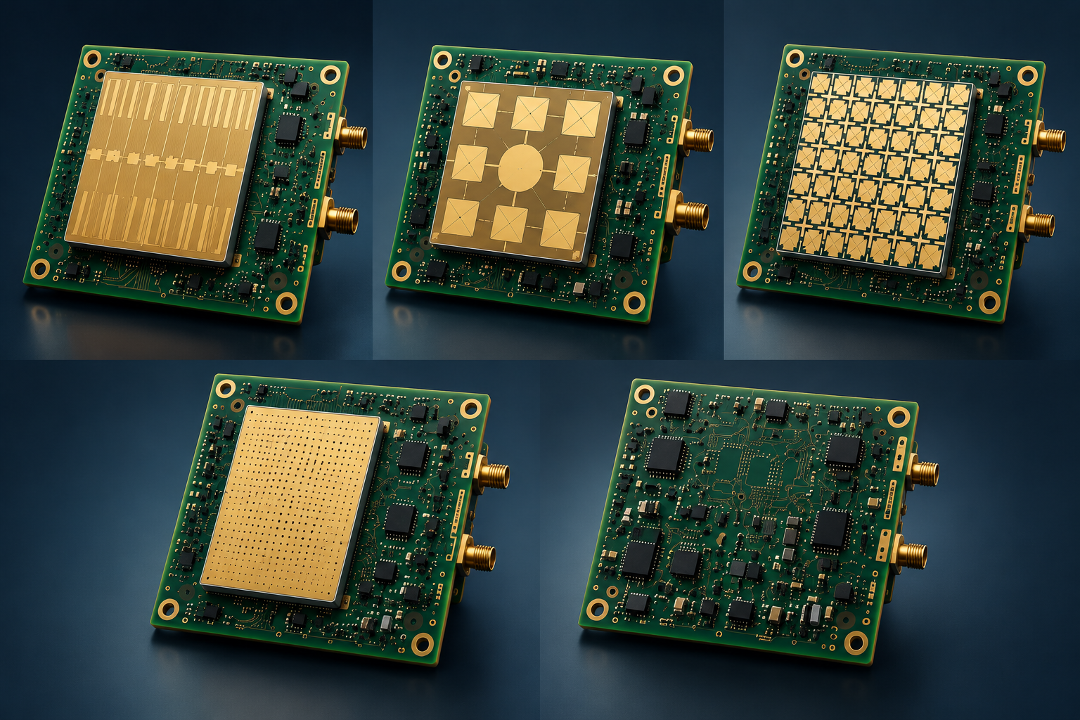
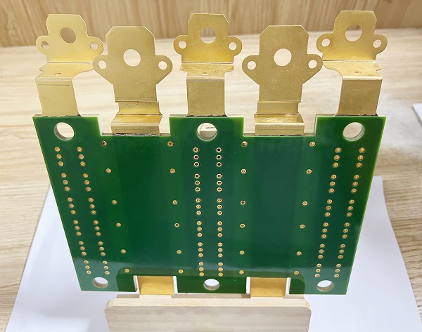
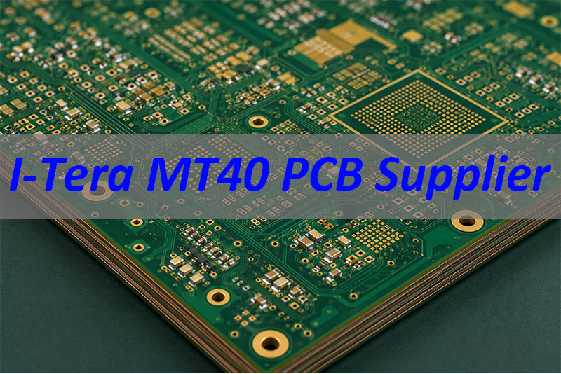
An I-Tera MT40 PCB supplier supports multilayer PCB projects that require Isola I-Tera MT40 material for low-loss, high-speed, RF-related, or radar electronic applications. This article explains how I-Tera MT40 is used in radar, RF-related, and high-speed multilayer PCB projects, and how EBest Circuit (Best Technology) supports manufacturability review, PCB fabrication, PCBA assembly, testing, and production traceability.
EBest Circuit (Best Technology) supports I-Tera MT40 multilayer PCB projects based on customer-provided Gerber files, stack-up requirements, impedance tables, drawings, BOM, and assembly needs. Our support includes DFM review, PCB layout support when complete customer inputs are available, stack-up manufacturability review, controlled impedance PCB fabrication, PCBA assembly, component sourcing, testing coordination, and MES-based production traceability. If you are working on an I-Tera MT40 radar PCB, RF-related PCB, or high-speed multilayer board, you can send your files and requirements to sales@bestpcbs.com for engineering review.
What Is I-Tera MT40 Multilayer PCB?
An I-Tera MT40 multilayer PCB is a printed circuit board made with Isola I-Tera MT40 laminate and prepreg in a multilayer structure. It is usually used when the board needs lower signal loss, better impedance stability, and more predictable performance than standard FR4.
In simple words, it is a multilayer PCB for demanding signal transmission.
It is commonly used when the project needs:
- Low-loss signal transmission
High-speed and RF-related signals can weaken as they travel through PCB traces. I-Tera MT40 helps reduce signal loss compared with many standard FR4 materials. - Stable impedance control
Radar, RF, and high-speed boards often require controlled impedance. Material, dielectric thickness, copper thickness, trace width, and stack-up must work together. - High-layer-count routing
Radar or communication boards may need many signal, ground, and power layers. 12-layer, 16-layer, or 20-layer structures are common in complex systems. - Reliable multilayer manufacturing
I-Tera MT40 can be used in multilayer stack-ups where stable lamination, material consistency, and repeatable production matter.
For example, a 20-layer PCB with Isola I-Tera MT40 material used in a radar project should first be understood as:
a 20-layer low-loss multilayer PCB for radar electronics.
Depending on the real circuit and structure, it may also be described as:
- Radar PCB if it supports radar signal or radar control functions;
- RF-related PCB if it includes RF or microwave signal sections;
- High-speed PCB if the main function is high-speed digital signal transmission;
- HDI PCB only if it includes HDI features such as laser microvias, blind vias, buried vias, or sequential lamination.
The material name alone does not decide the final category. The real classification depends on the application and board structure.
EBest Circuit (Best Technology) can review I-Tera MT40 multilayer PCB projects from a manufacturability perspective, including stack-up, impedance requirements, via structure, material use, surface finish, and testing needs.
Why Use I-Tera MT40 for High-Speed Multilayer PCB?
I-Tera MT40 is used in high-speed multilayer PCB projects because signal performance becomes harder to control as speed, frequency, layer count, and routing density increase.
For radar, RF-related, and high-speed electronic systems, the PCB material can directly affect signal behavior.
Key reasons to use I-Tera MT40 include:
- Lower dielectric loss
Lower loss helps signals pass through the PCB with less attenuation. This is useful for radar modules, communication boards, and long high-speed signal paths. - Stable Dk and Df performance
Stable dielectric properties help support more predictable impedance and signal transmission. - Suitable for multilayer structures
I-Tera MT40 is available as laminate and prepreg, which makes it suitable for multilayer stack-ups. - Good fit for controlled impedance boards
Many I-Tera MT40 projects require single-ended or differential impedance control. This material is often selected when impedance stability matters. - More practical processing than some special RF materials
Compared with some PTFE-based materials, I-Tera MT40 can be more practical for multilayer PCB fabrication.
For customers, the value is not just “using a better material.” The real value is using the material correctly.
A successful I-Tera MT40 multilayer PCB depends on:
- practical stack-up;
- controlled impedance;
- stable lamination;
- accurate drilling;
- reliable copper plating;
- proper surface finish;
- electrical testing;
- clear production documentation.
EBest Circuit (Best Technology) can review customer-provided files before production and help reduce avoidable risks in high-layer-count PCB fabrication and assembly.
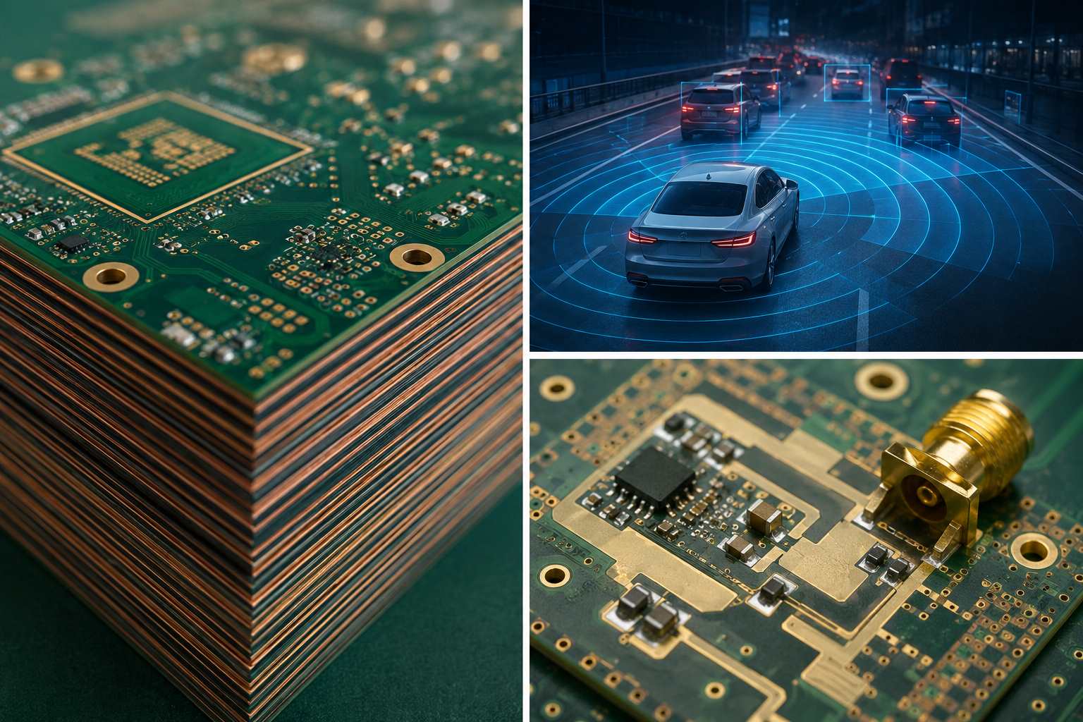
What Applications Need I-Tera MT40 Multilayer Boards?
I-Tera MT40 multilayer boards are often used in projects where signal quality, low loss, and high layer count matter. These applications usually require more manufacturing control than ordinary FR4 PCB projects.
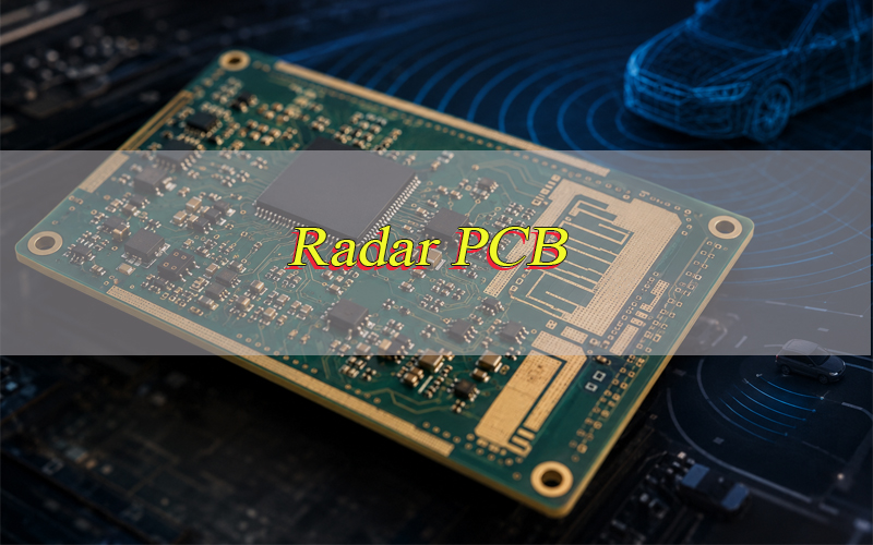
Radar Electronics
Radar electronics is one of the strongest application areas for I-Tera MT40 multilayer PCB.
Typical radar-related uses include:
- automotive radar modules;
- industrial radar sensing systems;
- radar control boards;
- RF signal processing boards;
- mixed RF and digital radar electronics.
Radar boards may combine RF signal paths, high-speed digital control sections, power layers, ground reference layers, and shielding structures in one multilayer PCB. This is why stack-up, impedance, material loss, and manufacturing consistency must be reviewed carefully.
A 20-layer I-Tera MT40 radar PCB is a good example. It is not just a “20-layer board.” It is a low-loss multilayer PCB where material choice, layer structure, via design, and impedance control all influence production quality.
Communication Equipment
Communication products often need dense routing, high-speed channels, and stable impedance.
Typical applications include:
- network equipment;
- base station electronics;
- optical communication control boards;
- signal processing boards;
- high-speed communication modules.
For these boards, multilayer structures help separate signal, power, and ground layers. I-Tera MT40 helps support lower loss in high-speed paths.
RF and Microwave Modules
I-Tera MT40 can be used in RF-related PCB projects when the design requires lower loss and controlled signal behavior.
Typical applications include:
- RF control boards;
- microwave support boards;
- antenna-related circuits;
- mixed RF and digital boards;
- high-frequency signal modules.
For RF-related boards, fabrication consistency matters. Dielectric thickness, copper profile, impedance, via design, and surface finish should all be reviewed before production.
High-Speed Digital Systems
High-speed digital systems may use I-Tera MT40 when standard FR4 cannot meet the signal loss target.
Typical applications include:
- server boards;
- backplanes;
- high-speed connector boards;
- FPGA boards;
- processor boards;
- SerDes signal boards.
In these projects, the board may not be called an RF PCB. It may be better classified as a high-speed low-loss multilayer PCB.
Industrial, Medical, Automotive, and Aerospace Electronics
High-reliability industries may use I-Tera MT40 when products require stable performance, better signal control, and reliable manufacturing.
Typical applications include:
- industrial control modules;
- medical electronic control boards;
- automotive electronics;
- aerospace communication boards;
- high-reliability signal control modules.
EBest Circuit (Best Technology) supports these projects through PCB fabrication, PCBA assembly, DFM review, testing coordination, and production traceability.
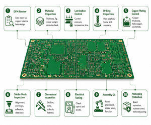
What Should Be Checked Before Manufacturing I-Tera MT40 Multilayer PCB?
Before manufacturing an I-Tera MT40 multilayer PCB, the supplier should not only check whether the material is available. The key is to confirm whether the board can be manufactured reliably.
Important items include:
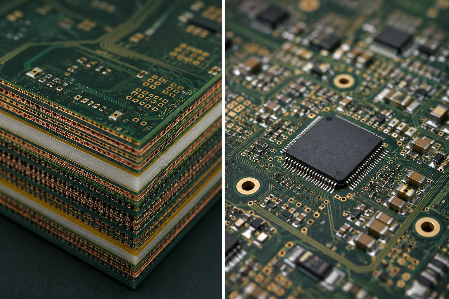
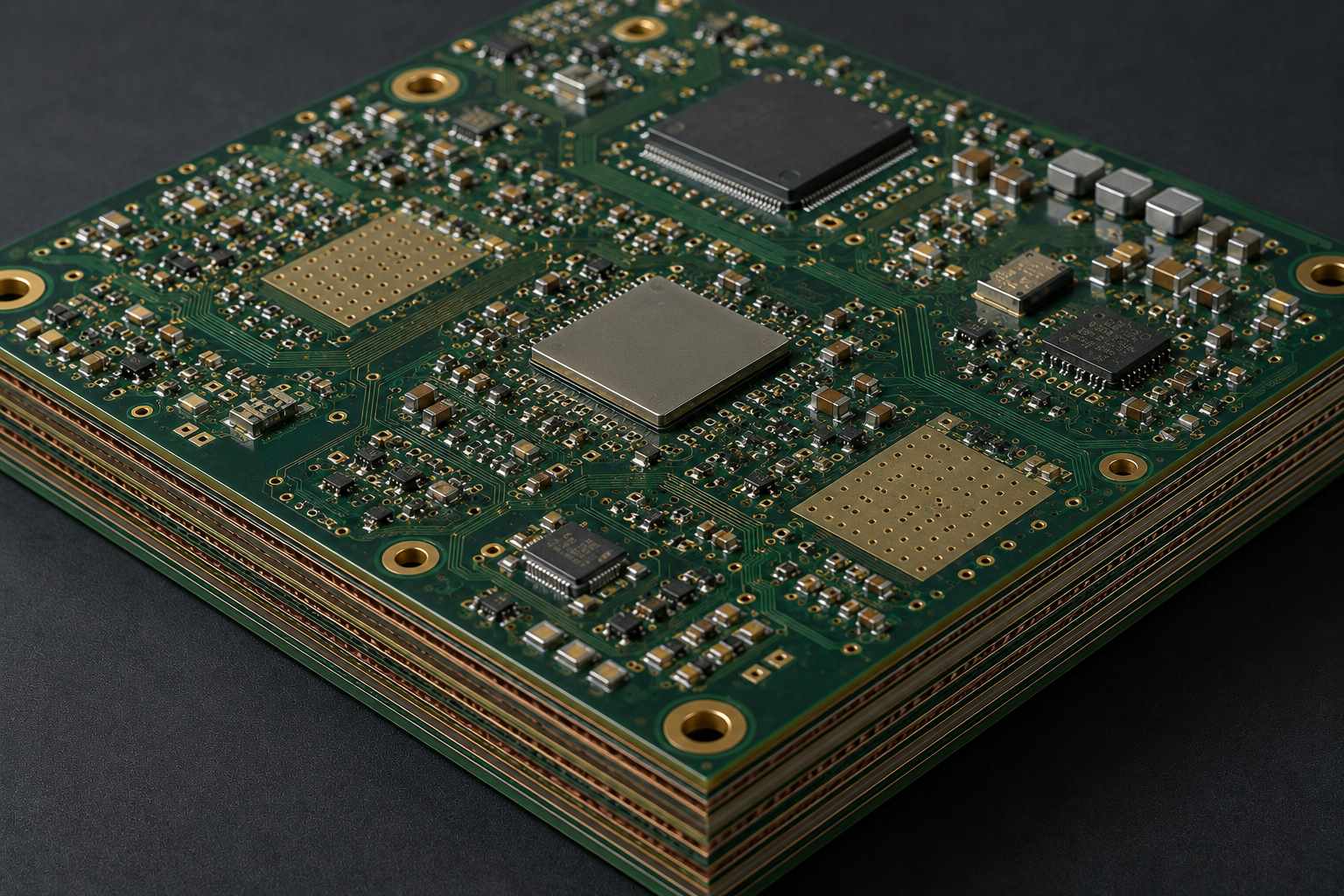
1. Layer Count
First confirm the layer count.
Common examples include:
- 8-layer I-Tera MT40 PCB;
- 12-layer I-Tera MT40 PCB;
- 16-layer I-Tera MT40 PCB;
- 20-layer I-Tera MT40 PCB;
- higher-layer-count multilayer PCB.
The higher the layer count, the more important these factors become:
- lamination control;
- layer-to-layer registration;
- board thickness control;
- drilling accuracy;
- copper plating reliability;
- impedance consistency.
For radar and high-speed applications, a high-layer-count board should be treated as a precision multilayer project, not a routine PCB job.
2. Stack-Up Manufacturability
Stack-up affects both electrical performance and manufacturing stability.
The supplier should review:
- core thickness;
- prepreg thickness;
- signal layer arrangement;
- ground reference layers;
- power layer arrangement;
- copper thickness;
- final board thickness;
- structure symmetry;
- dielectric spacing.
EBest Circuit (Best Technology) can review customer-provided stack-ups from a manufacturing perspective. We do not replace the customer’s product design, RF design, or circuit design work. Our role is to check whether the proposed stack-up is practical for PCB fabrication and assembly.
3. Controlled Impedance
Most I-Tera MT40 radar, RF-related, and high-speed boards need controlled impedance.
The review should include:
- target impedance;
- single-ended impedance;
- differential impedance;
- trace width;
- trace spacing;
- dielectric thickness;
- copper thickness;
- reference plane;
- tolerance requirement.
If the impedance target is not clearly defined, the board may be difficult to control during production. Customers should provide an impedance table whenever possible.
4. Via Structure
Via structure affects manufacturing difficulty, reliability, and cost.
The supplier should confirm whether the board uses:
- through holes;
- blind vias;
- buried vias;
- laser microvias;
- via-in-pad;
- resin plugging;
- copper filling;
- stacked vias;
- staggered vias.
This is also where the HDI question becomes clear.
A 20-layer I-Tera MT40 radar PCB is not automatically HDI.
It becomes HDI only when the customer’s design uses HDI structures such as laser microvias, blind/buried vias, or sequential lamination.
For this article, HDI is not the main topic. It is only a manufacturing structure that may appear in some I-Tera MT40 multilayer projects.
5. Drilling and Plating Quality
High-layer-count I Tera MT40 PCB requires stable drilling and plating.
Important checks include:
- minimum drill size;
- aspect ratio;
- hole wall quality;
- desmear process;
- copper plating thickness;
- annular ring;
- drill-to-copper clearance;
- reliability class.
Poor drilling or plating can cause serious reliability issues, especially in thick multilayer boards used for radar or high-speed applications.
6. Surface Finish
Surface finish should match assembly and product requirements.
Common options include:
- ENIG;
- ENEPIG;
- immersion silver;
- OSP;
- hard gold for connector areas.
For radar and RF-related boards, surface finish should also be reviewed for signal behavior, assembly method, storage conditions, and reliability requirements.
7. Testing Requirements
Testing should be defined before production.
Common tests and inspections include:
- electrical test;
- impedance test;
- AOI;
- X-ray inspection when needed;
- microsection analysis when required;
- solderability test;
- final visual inspection;
- functional testing after PCBA when required.
EBest Circuit (Best Technology) can support testing coordination based on the customer’s board requirements and application needs.
Can I-Tera MT40 Be Used in Hybrid Stackups?
Yes. I-Tera MT40 can be used in hybrid stackups when only certain layers need low-loss performance. This can help balance signal performance, material cost, and multilayer manufacturability.
Possible hybrid structures include:
- I-Tera MT40 for radar or RF-related signal layers
These layers handle sensitive signal paths where low loss and impedance stability matter. - FR4 or High-Tg FR4 for control or power layers
These layers may not need the same low-loss performance, so standard materials may be enough. - Other RF materials for special high-frequency sections
Some projects may combine different material systems based on frequency, signal type, and customer requirements.
Hybrid stackups should be reviewed carefully before production.
Key checks include:
- material compatibility;
- CTE behavior;
- lamination cycle;
- resin flow;
- dielectric thickness;
- impedance control;
- board warpage;
- reliability requirement.
EBest Circuit (Best Technology) can review hybrid stack-up manufacturability based on customer-provided drawings, stack-up, impedance table, and production requirements.
I-Tera MT40 vs FR4, Rogers, and PTFE for Multilayer PCB
Different PCB materials are used for different design needs. I-Tera MT40 is often selected when customers need better signal performance than standard FR4, while still keeping multilayer PCB manufacturing practical.
| Material | Best For | Key Point |
|---|---|---|
| Standard FR4 | Common multilayer PCB | Cost-effective, but higher loss |
| High-Tg FR4 | Reliable multilayer PCB | Better thermal resistance, not always low-loss |
| I-Tera MT40 | High-speed low-loss multilayer PCB | Balanced signal performance and processability |
| Rogers | RF and microwave PCB | Strong RF performance, higher cost |
| PTFE | Very high-frequency PCB | Good RF behavior, more difficult processing |
When Standard FR4 Is Enough
FR4 is suitable for many standard multilayer boards.
It may be enough when:
- signal speed is not very high;
- loss is not the main concern;
- cost control is the priority;
- impedance requirements are not too strict.
When High-Tg FR4 Is Better
High-Tg FR4 is suitable when thermal reliability matters more.
It is often used when:
- assembly temperature is higher;
- product reliability requirement is stricter;
- the board needs better heat resistance than standard FR4.
When I-Tera MT40 Makes Sense
I-Tera MT40 makes sense when signal performance is more important.
It is often used when:
- signal loss must be reduced;
- impedance control is critical;
- the board has radar or RF-related signal sections;
- the board has high-speed digital signals;
- the stack-up has many layers;
- the project needs a balance between performance and manufacturability.
When Rogers or PTFE May Be Needed
Rogers or PTFE materials may still be better for some specialized RF and microwave circuits.
They may be considered when:
- the frequency is very high;
- RF performance is the top priority;
- the customer has specified the material;
- the board requires a dedicated RF material system.
The right question is not simply “which material is best?”
The better question is:
Which material fits the radar signal, frequency range, stack-up, cost target, and manufacturing requirement?
EBest Circuit (Best Technology) can review customer-specified material requirements from a manufacturing perspective and provide PCB fabrication support based on manufacturability, material availability, and production needs.
Why Choose EBest Circuit as Your I-Tera MT40 PCB Supplier?
Choosing an I-Tera MT40 PCB supplier is not only about finding a company that can quote the material. For radar, RF-related, and high-speed multilayer boards, the supplier should understand high-layer-count PCB manufacturing, stack-up control, impedance, drilling, plating, testing, and assembly requirements.
EBest Circuit (Best Technology) supports customers in these practical areas:
I-Tera MT40 Multilayer PCB Fabrication
We can support I-Tera MT40 multilayer PCB fabrication based on customer drawings, Gerber files, stack-up, impedance table, and project requirements.
Typical project types include:
- high-speed multilayer PCB;
- radar multilayer PCB;
- low-loss PCB;
- RF-related PCB;
- controlled impedance PCB;
- high-layer-count PCB;
- hybrid stack-up PCB.
DFM and Stack-Up Manufacturability Review
Before production, our engineering team can review:
- stack-up manufacturability;
- line width and spacing;
- drill-to-copper clearance;
- via structure;
- copper balance;
- solder mask clearance;
- controlled impedance requirements;
- surface finish;
- final board thickness;
- testing requirements.
This review focuses on PCB manufacturing feasibility. It does not replace the customer’s product design, RF design, or circuit design work.
PCB Layout Support Based on Customer Inputs
EBest Circuit (Best Technology) can support PCB layout work when the customer provides the required design inputs, such as:
- schematic;
- netlist;
- component placement requirements;
- mechanical constraints;
- impedance requirements;
- routing rules;
- connector position requirements;
- keep-out areas;
- assembly requirements.
Our role is to help prepare or adjust manufacturable PCB layout files based on the customer’s design inputs. We do not position this service as full PCB design, circuit design, RF design, or product design.
Support for Multiple PCB Types
Besides I-Tera MT40 multilayer PCB, EBest Circuit (Best Technology) can support:
- FR4 PCB;
- High-Tg PCB;
- HDI PCB;
- heavy copper PCB;
- RF PCB;
- rigid-flex PCB;
- aluminum PCB;
- copper substrate PCB;
- ceramic PCB;
- multi-layer PCB;
- PCBA assembly projects.
This is useful for customers who have different board types within the same product platform.
PCBA Assembly and Component Sourcing
Many customers need more than bare PCB fabrication. They also need assembly and supply chain support.
EBest Circuit (Best Technology) can support:
- PCB fabrication;
- component sourcing;
- SMT assembly;
- through-hole assembly;
- assembly process review;
- testing coordination;
- prototype to batch production.
Testing and MES Traceability
For high-reliability projects, testing and traceability are important.
We can support:
- electrical testing;
- impedance testing;
- AOI inspection;
- X-ray inspection when needed;
- functional testing coordination;
- production quality documentation;
- MES-based production traceability.
These capabilities are valuable for radar, communication, industrial control, medical electronics, automotive electronics, aerospace, RF-related, and high-speed digital projects.
If you need an I-Tera MT40 multilayer PCB supplier for radar or high-speed applications, pls feel free to send your Gerber files, stack-up, BOM, impedance table, and requirements to sales@bestpcbs.com. Our team can review manufacturability, material requirements, assembly needs, testing requirements, and quotation details.
FAQs About I-Tera MT40 PCB Supplier
1. Is I-Tera MT40 suitable for multilayer PCB?
Yes. I-Tera MT40 is suitable for multilayer PCB designs that need low loss, controlled impedance, and stable high-speed signal performance.
2. Can I-Tera MT40 be used for radar PCB?
Yes. I-Tera MT40 can be used for radar-related multilayer PCB projects when the board requires low-loss material, controlled impedance, and stable signal transmission.
3. Can I-Tera MT40 be used for 20-layer PCB?
Yes. A 20-layer PCB using I-Tera MT40 can be manufactured as a high-speed low-loss multilayer PCB. If it is used in radar electronics, it can also be described as a 20-layer radar multilayer PCB. Final feasibility depends on stack-up, via structure, impedance requirement, board thickness, and manufacturing capability.
4. Is I-Tera MT40 PCB an RF PCB or high-speed PCB?
It depends on the application. If the board is used for RF or microwave circuits, it can be called RF PCB. If it is used for high-speed digital signals, it is better called high-speed PCB. If it is used in radar electronics, radar PCB or radar multilayer PCB may be more accurate.
5. Is a 20-layer I-Tera MT40 PCB automatically HDI?
No. A 20-layer board is a multilayer PCB. It becomes HDI only when the customer’s design includes HDI features such as laser microvias, blind vias, buried vias, stacked vias, or sequential lamination.
6. Can I-Tera MT40 be used with FR4 in hybrid stackups?
Yes. I-Tera MT40 can be used with FR4 or High-Tg FR4 in hybrid stackups when only certain layers need low-loss performance. The hybrid structure should be reviewed for material compatibility, lamination behavior, impedance control, and reliability.
7. What files are needed for an I-Tera MT40 multilayer PCB quotation?
Please provide:
- Gerber files;
- stack-up;
- fabrication drawing;
- impedance table;
- drill file;
- BOM if assembly is needed;
- surface finish requirement;
- copper thickness;
- board thickness;
- testing requirements;
- application notes if available.
8. Can EBest Circuit provide PCB design for I-Tera MT40 projects?
EBest Circuit (Best Technology) does not provide full PCB design, circuit design, RF design, or product design services. We can support PCB layout work when the customer provides the required design inputs, and we can review manufacturability for PCB fabrication and assembly.
9. Can EBest Circuit support I-Tera MT40 PCB fabrication and assembly?
Yes. EBest Circuit (Best Technology) can support I-Tera MT40 multilayer PCB fabrication, DFM review, stack-up manufacturability review, controlled impedance, PCBA assembly, component sourcing, testing coordination, and production traceability.
10. How can I get engineering support for an I-Tera MT40 PCB project?
Send your Gerber files, stack-up, impedance table, BOM, drawings, and requirements to sales@bestpcbs.com. EBest Circuit (Best Technology) will review PCB manufacturability, material requirements, assembly needs, testing requirements, and quotation details.
To sum up, an I Tera MT40 PCB supplier should provide more than a material-based quotation. For radar, RF-related, and high-speed multilayer boards, the real value is manufacturing control: stack-up manufacturability review, impedance control, lamination stability, drilling quality, copper plating reliability, testing, assembly support, and production traceability.
If your project is a 12-layer, 16-layer, 20-layer, or higher-layer PCB using Isola I-Tera MT40 material, it should be treated as a high-speed low-loss multilayer PCB from the beginning. If it is used in radar electronics, the supplier should pay extra attention to impedance, signal layers, via structure, material stability, and testing requirements. If it also includes laser microvias, blind vias, buried vias, or stacked vias, it may need HDI-level manufacturing review, but HDI is only part of the structure, not the main category.
EBest Circuit (Best Technology) supports I-Tera MT40 multilayer PCB projects from manufacturability review to PCB fabrication, PCBA assembly, testing, and production support. Send your files and project requirements to sales@bestpcbs.com for a practical review before production.