Any layer HDI PCB is designed for compact electronics that cannot be routed with standard multilayer PCB or ordinary HDI PCB. It supports stacked copper-filled microvias, fine-line routing, thin dielectric layers and complex layer-to-layer interconnection, making it suitable for fine-pitch BGA, high-speed modules and miniature electronic products.
For engineers, the main concern is whether the stackup, microvia structure, impedance control and material selection are manufacturable. For buyers, the key concerns are quotation accuracy, prototype lead time, batch consistency and supplier reliability. A professional manufacturer should solve both design risk and purchasing risk before fabrication starts.
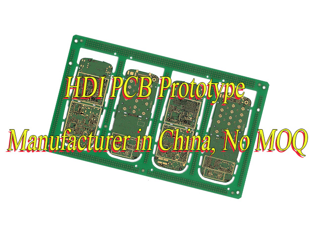
Are you worried about these problems in any layer HDI PCB projects?
- Delivery delays: Complex stackup review, sequential lamination, laser drilling, material lead time and repeated DFM corrections may slow down prototype and batch production.
- Hidden costs: Extra charges may appear after quotation, including copper-filled via processing, impedance control, material upgrades, additional inspection, stencil revision or SMT assembly adjustment.
- Quality instability: Stacked microvia cracks, weak copper filling, BGA soldering defects, warpage, impedance deviation or unstable surface finish may cause electrical failure, rework or field return risk.
As a China source factory with 20+ years PCB manufacturing experience, EBest Circuit provides solutions to above problems as below:
- Delivery predictability: Early stackup review, material planning, engineering confirmation and production tracking help reduce repeated changes before fabrication.
- Cost transparency: Quotation can cover PCB fabrication, prototype production, copper-filled microvias, surface finish, SMT assembly, testing, packaging and export documentation.
- Quality reliability: AOI, X-ray, flying probe test, impedance test, microsection, thermal stress test and functional testing help control HDI PCB quality from prototype to batch production.
Welcome to contact us if you have any request for any layer HDI PCB manufacturing and assembly: sales@bestpcbs.com.
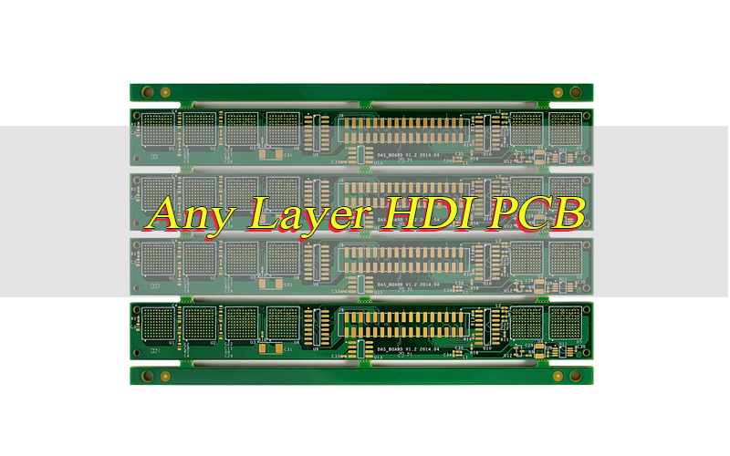
What Is Any Layer HDI PCB?
Any layer HDI PCB is an advanced HDI PCB structure that uses laser microvias to connect almost every layer of the circuit board. It is also called ELIC PCB, which means Every Layer Interconnect PCB.
This structure uses stacked copper-filled microvias, thin dielectric layers, fine traces and sequential lamination. It is designed for compact products where standard multilayer PCB or standard HDI PCB cannot provide enough routing space.
The main value of any layer HDI PCB is simple: it helps place more circuits in a smaller board area. It also shortens signal paths and supports complex layer-to-layer routing for fine-pitch BGA, high-speed chips and miniature electronic devices.
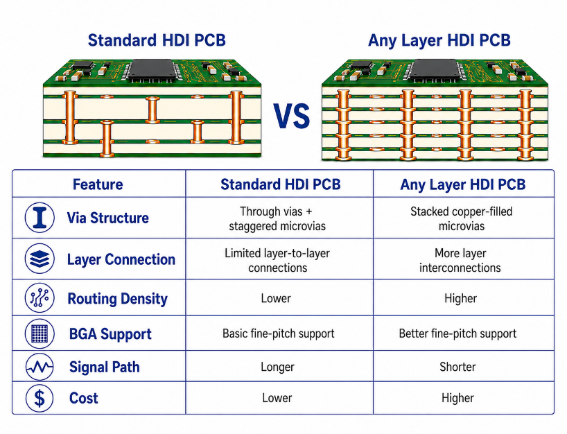
Any Layer HDI vs Standard HDI PCB: What Is the Difference?
The main difference is routing freedom. Standard HDI PCB usually uses limited blind vias, buried vias or build-up structures such as 1+N+1 and 2+N+2. Any layer HDI PCB uses stacked copper-filled microvias, so signals can move between layers more directly.
Standard HDI is usually better for medium-density products with controlled cost. Any layer HDI PCB is better for compact, high-density and high-speed products where routing space is limited. It costs more, but it gives stronger BGA escape capability, shorter signal paths and better miniaturization potential.
| Item | Standard HDI PCB | Any Layer HDI PCB |
|---|---|---|
| Via structure | Limited blind vias and buried vias | Stacked copper-filled microvias |
| Layer connection | Partial layer interconnection | Almost every layer can be interconnected |
| Common stackup | 1+N+1, 2+N+2 | ELIC / every layer interconnect |
| Routing density | Medium to high | Very high |
| BGA support | Suitable for larger or moderate-pitch BGA | Better for fine-pitch BGA and CSP |
| Signal path | May need longer routing | Shorter layer-to-layer transition |
| Board size | May require larger PCB area | Helps reduce PCB size |
| Lamination cycles | Fewer cycles | More sequential lamination cycles |
| Manufacturing difficulty | Moderate | High |
| Cost level | Lower | Higher |
| Reliability focus | General HDI process control | Stacked microvia reliability |
| Best use | Medium-density electronics | Compact, high-density and high-speed electronics |
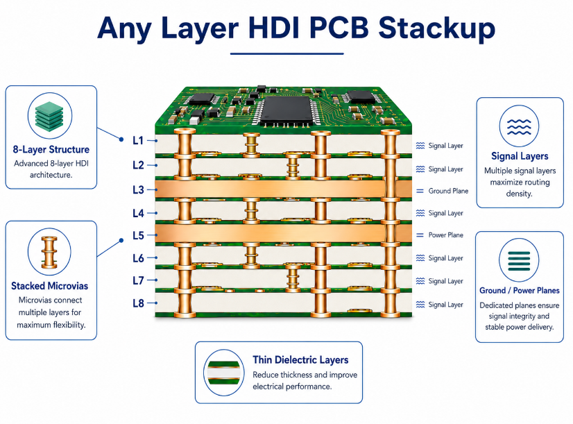
What Is the Stackup Structure of Any Layer HDI PCB?
Any layer HDI PCB stackup is built with multiple copper layers, thin dielectric layers and stacked copper-filled microvias. Unlike standard HDI, the microvias can be built layer by layer, allowing almost every layer to connect with another layer.
A typical stackup may have 6 layers, 8 layers, 10 layers, 12 layers or more. Each build-up layer is laser drilled, copper filled, planarized and laminated again. This repeated process creates a compact vertical interconnection structure.
A good stackup should balance signal layers, ground planes, power planes, dielectric thickness, copper thickness and microvia placement. If the stackup is too aggressive, the board may face plating stress, lamination misalignment, warpage or low yield.
| Stackup Type | Example Structure | Typical Use |
|---|---|---|
| 6-layer any layer HDI | L1-L2-L3-L4-L5-L6 with stacked microvias | Compact modules, small BGA |
| 8-layer any layer HDI | Every layer connected through filled microvias | IoT, RF and wearable devices |
| 10-layer any layer HDI | Signal, power and ground layers combined | Medical and industrial control boards |
| 12-layer any layer HDI | Dense signal layers with controlled impedance | Automotive and communication modules |
| 14+ layer any layer HDI | Complex high-speed multilayer structure | Advanced computing and high-reliability systems |
In real projects, the stackup should be confirmed before layout starts. This helps avoid unbuildable microvia structures, unstable impedance and unnecessary cost increases.
What Thickness Options Are Available for Any Layer HDI PCB?
Common any layer HDI PCB thickness ranges from 0.4 mm to 2.0 mm, depending on layer count, stackup design and mechanical requirements. Ultra-thin boards are used for compact devices, while thicker boards are selected for connectors, rigidity and stronger mechanical support.
Thickness must be reviewed together with microvia depth, copper weight, dielectric thickness and assembly warpage risk. A thinner board helps miniaturization, but it can increase handling difficulty during lamination, routing, SMT assembly and reflow. For stable batch production, thickness should balance space, reliability and process yield.
| Thickness | Typical Use | Design Note |
|---|---|---|
| 0.4 mm | Wearables, compact modules | Higher handling control |
| 0.6 mm | Sensor boards, small electronics | Good miniaturization |
| 0.8 mm | IoT modules, RF boards | Balanced option |
| 1.0 mm | Industrial compact electronics | Better rigidity |
| 1.2 mm | Communication modules | Stable assembly |
| 1.6 mm | Control boards, embedded systems | Common thickness |
| 2.0 mm | High-strength designs | More mechanical support |
What Microvia Size Is Used in Any Layer HDI PCB?
Typical any layer HDI PCB microvia diameter is 0.075 mm to 0.15 mm, while pad diameter is often 0.20 mm to 0.30 mm. The final value depends on dielectric thickness, laser drilling capability, plating quality and reliability requirements.
Smaller microvias provide higher routing density, but they also increase manufacturing difficulty. For stacked microvias, copper filling, plating uniformity and thermal stress control are critical. Before layout is finalized, the microvia size should be reviewed with the PCB manufacturer to avoid low yield, weak interconnection or later redesign.
| Parameter | Typical Value |
|---|---|
| Laser microvia diameter | 0.075–0.15 mm |
| Microvia pad diameter | 0.20–0.30 mm |
| Microvia depth | 0.05–0.10 mm |
| Preferred aspect ratio | ≤0.75:1 |
| Via filling | Copper filled |
| BGA via-in-pad | Available |
For high-reliability projects, microvia design should not be pushed to the smallest possible size without purpose. The better approach is to choose the smallest structure that still leaves safe manufacturing margin.
What Minimum Trace Width and Spacing Can Any Layer HDI PCB Support?
Any layer HDI PCB commonly supports 50–75 μm trace width and spacing, depending on copper thickness, material, etching control and yield target. Some advanced fine-line HDI PCB projects may use tighter values, but the actual capability must be confirmed case by case.
Fine lines help route dense BGA and reduce board size. However, very narrow spacing increases the risk of etching variation, impedance deviation, solder mask bridge issues and lower production yield. For mass production, the design should not only pursue the smallest value but also leave enough process margin.
| Item | Typical Value |
|---|---|
| Standard fine line | 75/75 μm |
| Advanced fine line | 50/50 μm |
| BGA escape routing | 50–75 μm |
| Copper thickness | 12–35 μm |
| Impedance tolerance | ±10% typical |
| Solder mask bridge | Project-dependent |
Therefore, minimum trace width should be selected based on real product goals. A slightly wider rule may improve yield, reduce cost and make batch production more stable.
What Materials Should Be Selected for Any Layer HDI PCB?
Any layer HDI PCB materials should be selected based on signal speed, dielectric thickness, thermal stress and lamination reliability. Standard FR4 may work for low-speed compact boards, while high-speed, RF or high-reliability projects often require high-Tg, low-Dk or low-Df laminate.
Material selection affects laser drilling quality, copper adhesion, CAF resistance, dimensional stability, impedance control and reflow reliability. Before production, EBest Circuit can review material availability, stackup symmetry, Tg, Dk, Df and lead time to reduce prototype delays and batch variation.
| Material Factor | Recommended Focus |
|---|---|
| Tg | ≥170°C for higher reliability |
| Dk | Stable value for impedance control |
| Df | Lower value for high-speed loss control |
| CTE | Lower Z-axis expansion |
| CAF resistance | Important for fine spacing |
| Dimensional stability | Important for registration |
| Lead time | Important for prototype schedule |
For global OEM projects, material selection should also consider long-term supply stability. A material that is technically suitable but difficult to source may delay future batch production.
How to Design Any Layer HDI PCB?
Any layer HDI PCB design should start with stackup planning, not routing. The stackup affects BGA escape, microvia depth, impedance control, material selection, cost and manufacturing reliability.
Step 1: Confirm component density and BGA pitch.
Fine-pitch BGA, CSP and dense connectors decide whether via-in-pad, stacked microvias and fine-line routing are needed. The BGA escape plan should be confirmed before detailed layout.
Step 2: Define the stackup with the PCB manufacturer.
Layer count, dielectric thickness, copper thickness, signal layers, ground planes and power planes should be reviewed together. This helps prevent impedance mismatch, poor lamination balance and unbuildable microvia structures.
Step 3: Use manufacturable microvia rules.
Typical laser microvia diameter is 0.075–0.15 mm, and the preferred microvia aspect ratio is usually ≤0.75:1. Avoid unnecessary tall stacked vias because they increase plating stress and reliability risk.
Step 4: Control trace width and spacing.
Common fine-line capability is 50–75 μm. Very tight lines improve routing density, but they may reduce production yield. For batch production, the design should keep enough manufacturing margin.
Step 5: Protect high-speed signal paths.
Keep critical signals close to continuous ground reference planes. Avoid return path gaps, excessive layer transitions and poorly controlled differential pair spacing.
Step 6: Balance copper distribution.
Uneven copper distribution may cause lamination pressure imbalance and board warpage. Copper balance should be checked across signal layers, power layers and ground layers.
Step 7: Review assembly risk before fabrication.
Via-in-pad flatness, BGA pad size, solder mask bridge, stencil design and reflow warpage should be checked early. A good HDI design must be easy to manufacture and stable during SMT assembly.
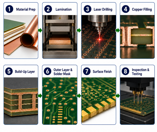
How Does the Any Layer HDI PCB Manufacturing Process Work?
Any layer HDI PCB manufacturing uses repeated lamination, laser drilling, copper filling and plating to build every layer interconnection. Each build-up cycle must be accurately controlled because small errors may affect microvia alignment and final reliability.
Step 1: Material preparation and inner layer imaging.
The process starts with laminate, copper foil and prepreg preparation. Inner layers are imaged, etched and inspected to confirm circuit accuracy before lamination.
Step 2: Inner core lamination.
The inspected inner layers are laminated under controlled temperature, pressure and time. Stable lamination is important because later microvia alignment depends on dimensional stability.
Step 3: Laser microvia drilling.
Laser drilling creates small microvias between adjacent layers. The process must control via diameter, depth and position accuracy.
Step 4: Desmear, plating and copper filling.
After drilling, the microvias are cleaned, plated and copper filled. Copper filling creates a solid vertical connection and prepares a flat surface for stacked microvia construction.
Step 5: Planarization and next build-up layer.
The filled microvias are planarized. Then the next dielectric and copper layer are laminated. The same drilling, filling and plating process is repeated layer by layer.
Step 6: Outer layer imaging and solder mask.
After the full stackup is completed, the outer circuit is formed. Solder mask is applied to protect copper areas and define soldering pads.
Step 7: Surface finish and profiling.
ENIG, ENEPIG or other surface finishes are applied based on assembly and reliability requirements. The board is then routed or profiled to final size.
Step 8: Final inspection and testing.
Electrical testing, AOI, X-ray, microsection, impedance testing and reliability inspection are used to confirm that the HDI board meets project requirements.
How Does Any Layer HDI PCB Improve Signal Integrity?
Any layer HDI PCB improves signal integrity by shortening signal paths and reducing unnecessary through-hole via stubs. In high-speed circuits, long traces, poor return paths and via stubs may cause reflection, crosstalk, insertion loss and timing problems.
With stacked microvias, signals can move between layers more directly. This helps designers keep critical traces close to ground planes, reduce loop area and create cleaner return paths. It is especially useful for fine-pitch BGA, RF modules and compact high-speed circuits.
However, HDI structure alone does not guarantee good signal integrity. The stackup must still control dielectric thickness, impedance, copper roughness, differential pair spacing, via transition and reference plane continuity.
Good signal integrity design should focus on:
- Shorter interconnect paths to reduce signal delay and loss.
- Continuous reference planes to keep return current stable.
- Controlled impedance to reduce reflection.
- Fewer through-hole via stubs to improve high-speed performance.
- Proper differential pair routing to control skew and crosstalk.
- Stable material selection to reduce dielectric loss.
- Clean power and ground structure to reduce noise coupling.
For high-speed any layer HDI PCB projects, signal integrity should be reviewed during stackup design. Waiting until prototype testing may lead to redesign, delayed delivery and higher total cost.
What Applications Commonly Use Any Layer HDI PCB?
Any layer HDI PCB is used in electronics where size, routing density and performance are critical. It is especially useful when the product contains fine-pitch BGA, high-speed chips, RF sections, dense connectors or strict mechanical space limits.
Common applications include:
- Smartphones, tablets and wearable electronics
- IoT modules and compact wireless devices
- Medical monitoring and diagnostic electronics
- Automotive sensor modules and control boards
- Communication modules and high-speed networking devices
- Industrial control boards with compact form factors
- Aerospace and defense electronics
- Camera modules and miniature embedded systems
These applications share one requirement: more reliable interconnections in a smaller PCB area. Therefore, the board should be reviewed as a complete product platform, not only as a bare PCB.
What Reliability Tests Are Required for Any Layer HDI PCB?
Any layer HDI PCB requires strict reliability testing because stacked microvias carry critical layer-to-layer connections. Testing should verify plating quality, microvia strength, impedance stability, solderability and assembly reliability.
Key reliability tests include:
- AOI inspection: Detects opens, shorts, line defects, spacing problems and etching errors before final shipment.
- Flying probe test: Verifies electrical continuity and isolation, especially for prototype and small-batch HDI PCB orders.
- Impedance test: Confirms whether controlled impedance traces meet the target tolerance, commonly ±10% depending on project requirements.
- X-ray inspection: Checks copper-filled microvias, via-in-pad areas and BGA solder joints after assembly.
- Microsection analysis: Verifies copper plating thickness, via filling quality, lamination structure and microvia connection reliability.
- Thermal stress test: Evaluates whether stacked microvias can survive heat exposure, reflow and temperature change.
- Solderability test: Confirms whether the surface finish can support stable SMT assembly and BGA soldering.
- Ionic contamination test: Checks board cleanliness to reduce leakage, corrosion and long-term reliability risk.
- Functional test: Verifies the assembled PCBA under real working conditions when assembly service is included.
For automotive, medical, aerospace or long-life industrial products, buyers should also confirm material traceability, inspection records, test reports and production process control before batch production.
How Much Does Any Layer HDI PCB Cost?
Any layer HDI PCB costs more than standard HDI PCB because it uses more lamination cycles, laser drilling, copper filling, tighter registration and advanced inspection. The final price depends on design difficulty, material choice, quantity, testing level and assembly scope.
Main cost factors include:
- Layer count: More layers increase material use, lamination time and inspection workload.
- Lamination cycles: Any-layer structures need repeated build-up processing, which increases production time and cost.
- Microvia structure: Stacked copper-filled microvias cost more than simple blind vias because plating and filling control are stricter.
- Trace width and spacing: Fine-line rules such as 50/50 μm require tighter process control and may reduce yield.
- Material grade: High-Tg, low-Dk or low-Df materials cost more than standard FR4, but they may be necessary for high-speed or high-reliability products.
- Surface finish: ENIG and ENEPIG are more expensive than HASL, but they are better for fine-pitch BGA and flat soldering pads.
- Testing requirements: X-ray, impedance testing, microsection and thermal stress testing increase cost but reduce quality risk.
- Assembly scope: SMT assembly, BGA soldering, stencil, functional testing and packaging should be included when calculating total project cost.
- Order quantity: Prototype cost per piece is higher because engineering review, tooling and setup costs are shared by fewer boards.
A fixed any layer HDI PCB pricelist is usually not accurate before DFM review. For a reliable quotation, buyers should provide Gerber or ODB++ files, stackup requirements, material preference, quantity, surface finish, impedance requirements and assembly scope.
What Services Can EBest Circuit Provide for Any Layer HDI PCB Projects?
EBest Circuit provides one-stop support for any layer HDI PCB projects, covering design, prototype, production, sourcing and assembly.
- PCB Design: Review stackup, microvia structure, BGA escape, fine-line routing and manufacturability before fabrication.
- PCB Prototype: Validate microvia reliability, impedance control, material selection and assembly risk before batch production.
- Mass Production: Support stable repeat orders with controlled process planning and production management.
- Component Sourcing: Help coordinate BOM, component matching and PCBA preparation.
- PCB Assembly: Provide SMT assembly, BGA soldering, X-ray inspection and functional testing.
- Engineering Support: Reduce redesign risk, DFM issues, hidden cost and prototype-to-production differences.
What Quality Certifications Support EBest Circuit’s HDI PCB Manufacturing?
EBest Circuit supports HDI PCB manufacturing with certified quality systems and global compliance requirements.
- ISO 9001:2015: Supports stable quality management and repeatable production control.
- IATF 16949: Supports automotive electronics projects with stricter process control and traceability.
- ISO 13485:2016: Supports medical electronics manufacturing quality requirements.
- AS9100D: Supports aerospace and high-reliability electronic projects.
- UL: Supports material safety, traceability and compliance review.
- RoHS: Supports restricted substance compliance for global electronics markets.
- REACH: Supports chemical compliance requirements for export projects.
These certifications help strengthen process control, material traceability, inspection records and long-term production stability for any layer HDI PCB manufacturing.
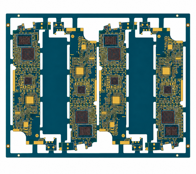
Any Layer HDI PCB Manufacturing Cases from EBest Circuit
Project Background
A wearable medical electronics project required a compact control board with a fine-pitch BGA, dense signal routing and strict size limits. The original design used standard HDI routing, but the available escape channels were not enough. The board also needed stable signal performance, reliable SMT assembly and repeatable production after prototype approval.
Project Requirements
The project required an 8-layer any layer HDI PCB with stacked copper-filled microvias, microvia-in-pad for BGA escape and controlled impedance routing. Key requirements included 0.10 mm laser microvias, 50/50 μm fine-line routing, ENIG surface finish, BGA X-ray inspection, impedance test coupons and functional testing after assembly.
EBest Circuit Solution
EBest Circuit reviewed the stackup, dielectric thickness, copper balance, BGA escape path and assembly risk before fabrication. The team adjusted the microvia structure to reduce unnecessary stacked via stress, optimized copper distribution to reduce warpage risk and confirmed the impedance model before production. PCB fabrication, component sourcing, SMT assembly, X-ray inspection and functional testing were coordinated in one project flow.
Output Results
The prototype passed 100% flying probe testing, BGA X-ray inspection and functional testing. Controlled impedance was verified within the project tolerance target of ±10%. The final board achieved stable BGA assembly, reduced routing congestion and supported a smoother transition from prototype to small-batch production. This case shows how early engineering review, HDI process control and assembly coordination can reduce redesign risk for complex any layer HDI PCB projects.
Why Choose EBest Circuit as China Any Layer HDI PCB Manufacturer?
EBest Circuit helps make any layer HDI PCB projects easier to move from design review to prototype, assembly and batch production. For complex HDI boards, the real value is not only fabrication capability, but also lower redesign risk, clearer cost control and more stable production quality.
- Reduce design and DFM risk: Stackup, microvia structure, BGA escape, fine-line routing, impedance control and assembly feasibility can be reviewed before production, helping reduce redesign and repeated engineering changes.
- Shorten prototype-to-production time: PCB design review, prototype fabrication, mass production, component sourcing and PCB assembly can be handled in one project flow, reducing communication gaps between different suppliers.
- Control total project cost: Early review helps identify risky microvia structures, material mismatch, excessive fine-line rules and unnecessary process upgrades before quotation is locked.
- Support urgent and batch orders: With strong monthly PCB production capability and expedited service, EBest Circuit can support urgent prototype demand and stable repeat production when project requirements are confirmed.
- Improve HDI PCB assembly reliability: SMT assembly, BGA soldering, X-ray inspection and functional testing help reduce solder voids, via-in-pad issues, reflow problems and final PCBA failure risk.
- Strengthen quality confidence: ISO 9001, IATF 16949, ISO 13485, AS9100D, UL, RoHS and REACH support process control, material traceability and compliance needs for global electronics projects.
- Work with one China source factory: PCB fabrication, HDI engineering support, component sourcing, assembly, testing and shipment can be coordinated together, reducing handoff risk and improving project control.
For any layer HDI PCB projects with fine-pitch BGA, stacked microvias, controlled impedance or compact layout requirements, EBest Circuit provides a practical manufacturing path from engineering review to finished PCBA.
FAQs About Any Layer HDI PCB
Q1: What files should be prepared before requesting an any layer HDI PCB quote?
A1: A useful quotation should include Gerber or ODB++ files, drill files, stackup drawing, impedance requirements, material preference, copper thickness, surface finish, quantity and assembly scope. If BOM and CPL files are available, the supplier can also review SMT assembly risk earlier.
Q2: Why is DFM review important before any layer HDI PCB production?
A2: DFM review helps find unbuildable stackups, risky microvia structures, tight spacing issues, poor copper balance and assembly risks before production. This reduces repeated engineering changes, hidden cost and prototype delay.
Q3: Can any layer HDI PCB be used for both prototype and mass production?
A3: Yes. The key is to keep stackup, material, microvia structure, impedance rules, surface finish and testing standards consistent from prototype to batch production. This helps reduce variation after sample approval.
Q4: What is the best surface finish for fine-pitch BGA on any layer HDI PCB?
A4: ENIG is commonly used because it provides flat pads, good solderability and stable BGA assembly support. ENEPIG may be selected for higher reliability or special bonding requirements. HASL is usually not preferred for dense HDI layouts.
Q5: Why does via-in-pad need copper filling in any layer HDI PCB?
A5: Via-in-pad normally needs copper filling and planarization to create a flat soldering surface. Without proper filling, solder may flow into the via, causing weak joints, voids or BGA assembly defects.
Q6: How can stacked microvia failure be reduced?
A6: Stacked microvia failure can be reduced by using proper aspect ratio, stable copper filling, controlled plating thickness, balanced stackup design and thermal stress testing. Avoiding unnecessary tall via stacks also helps improve reliability.
Q7: Is any layer HDI PCB suitable for high-speed interfaces?
A7: Yes, it can support high-speed interfaces when the stackup controls impedance, dielectric thickness, reference planes, copper roughness and via transitions. The design should be reviewed before prototype production to avoid signal integrity problems.
Q8: What is the main risk when choosing the lowest any layer HDI PCB price?
A8: The lowest price may hide risks such as weak microvia filling, limited inspection, unstable material sourcing, poor impedance control or assembly failure. For complex HDI boards, total project cost matters more than bare PCB unit price.
Q9: Can EBest Circuit support any layer HDI PCB assembly?
A9: Yes. EBest Circuit can support PCB fabrication, component sourcing, SMT assembly, BGA soldering, X-ray inspection and functional testing. This helps reduce handoff risk between PCB production and PCBA assembly.
Q10: What industries commonly require strict any layer HDI PCB traceability?
A10: Automotive, medical, aerospace, industrial control and communication electronics often require stricter traceability. Important records may include material lot data, production traveler records, inspection reports, microsection results and test documentation.
Q11: How can any layer HDI PCB lead time be shortened?
A11: Lead time can be shortened by confirming stackup, material, microvia rules, surface finish, testing plan and assembly files before order release. Clear files reduce DFM back-and-forth and help production start faster.
Q12: What should be checked before moving from prototype to batch production?
A12: Before batch production, check prototype test results, impedance reports, X-ray results, microsection records, solderability, functional testing and BOM stability. The approved prototype should match the planned mass production process.
Q13: Does any layer HDI PCB require special material selection?
A13: Yes. Material should match signal speed, Tg, Dk, Df, CTE, CAF resistance, thickness control and long-term availability. For high-speed or high-reliability products, standard FR4 may not always be the best option.
Q14: How do I know if my project really needs any layer HDI PCB?
A14: This structure is suitable when standard HDI cannot handle fine-pitch BGA escape, compact layout, high-density routing, short signal paths or strict product size limits. If standard HDI can meet the design, it may be more cost-effective.
Q15: What makes EBest Circuit suitable for any layer HDI PCB projects?
A15: EBest Circuit supports PCB Design, PCB Prototype, Mass Production, Component Sourcing and PCB Assembly. With 20+ years of PCB manufacturing experience, certified quality systems and one-stop project support, it can help reduce technical, production and assembly risk.
Get a Fast Quote for Your Any Layer HDI PCB Project
Any layer HDI PCB is a strong solution for compact products that require fine-pitch BGA routing, stacked copper-filled microvias, controlled impedance and reliable assembly. The key is not only making smaller vias, but building a manufacturable stackup that can stay stable through prototype, SMT assembly, inspection and batch production.
For purchasing, compare more than unit price. Review the supplier’s HDI engineering capability, microvia process control, material support, assembly service, testing method and quality documentation. If you need any layer HDI PCB design review, prototype production, PCB fabrication, component sourcing or assembly service, contact EBest Circuit for a clear quotation: sales@bestpcbs.com.