In the world of electronics, printed circuit boards (PCBs) play a vital role in connecting and powering various components. They are the backbone of every electronic device, from smartphones to industrial machinery. When it comes to designing a PCB for a project, the thickness of the copper layer is an important consideration. Heavy Copper PCB, also known as Thick Copper PCB, has become increasingly popular in charging automotives due to their unique features and benefits. In this article, we will discuss why consider heavy copper PCBs for your high current project.
What a Heavy Copper PCB is?
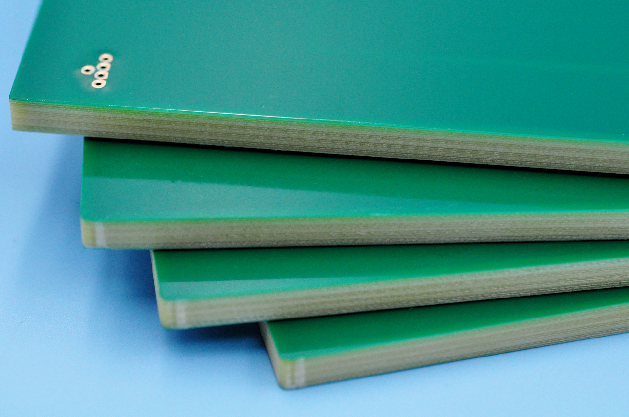
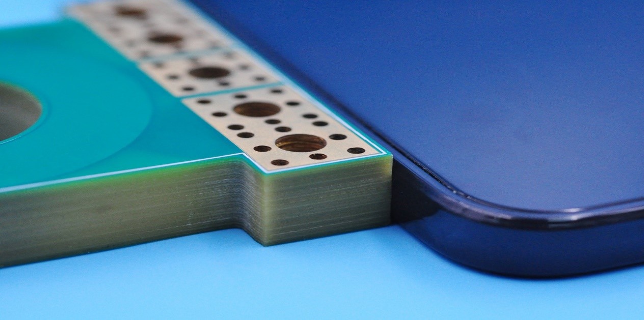
A heavy copper PCB is a circuit board with an unusually thick copper layer, usually exceeding 3 ounces per square foot (oz/ft²). By comparison, standard PCBs typically have a copper layer thickness of 1 oz/ft². Heavy copper PCBs are used in applications where high current is needed, or the board needs to withstand mechanical and thermal stress.
Benefits of Heavy Copper PCBs
- High Current Capacity
The thicker copper layer in a heavy copper PCB allows for a higher current capacity. This makes it ideal for high-power applications such as power supplies, motor controllers, and industrial equipment. Heavy copper PCBs can carry up to 20 amps or more, compared to the standard 5-10 amps of a regular PCB.
- Thermal Management
Heavy copper PCBs are known for their excellent thermal management capabilities. The thicker copper layer allows for better heat dissipation, reducing the risk of overheating and component failure. So that they can generate a lot of heat for the end-application.
- Durability
Heavy copper PCBs are more robust and durable than standard PCBs. The thicker copper layer provides better mechanical support, making them resistant to damage from vibration, shock, and bending. This makes them suitable for harsh environments and industrial applications.
- Increased Flexibility
Heavy copper PCBs offer increased design flexibility compared to standard PCBs. The thicker copper layer allows for more complex and compact designs, reducing the overall size of the board. This makes them ideal for applications where space is limited, that means you can make a very heavy copper while the size is very small.
- Better Signal Integrity
The thicker copper layer in heavy copper PCBs provides better signal integrity. This reduces the risk of signal loss and interference, resulting in more reliable and efficient circuit performance.
Copper thickness design for a Heavy Copper PCB?
Due to the thickness of copper in heavy copper PCB is thick then normal FR4 PCB, then it is easily to be warped if the copper thickness is not match each other in symmetrical layers. For example, if you are designing an 8 layers heavy copper PCB, then the copper thickness in each layer should follow L8=L1, L7=L2, L6=L3, L5=L4 standard.
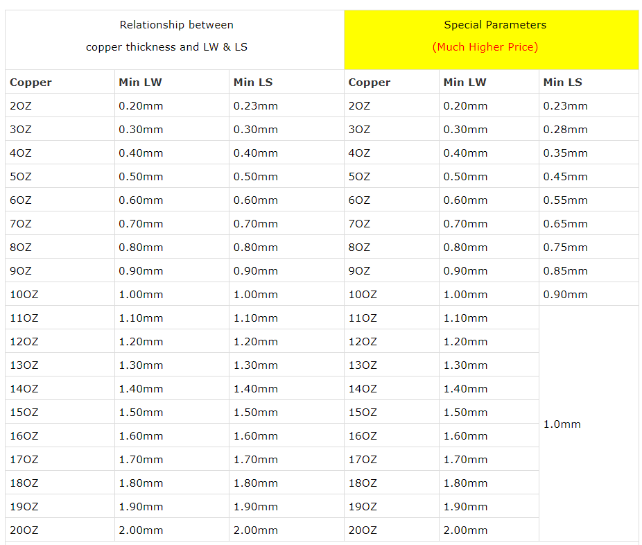
Additionally, the relationship between minimum line space and minimum line width also should be considered, follow the design rule will help to smooth production and shorten the lead time. Below are the design rules between them, LS refers to line space and LW refers to line width.
Drill hole rules for heavy copper board
A plated through hole (PTH) in printed circuit board is to connect top and bottom side to make them electricity. And when the PCB design has multi copper layers, the parameters of holes must be considered carefully, especially hole diameters.
In EBest Circuit (Best Technology), the minimum PTH diameter should be >=0.3mm while the copper ring annular should be 0.15mm at least. For wall copper thickness of PTH, 20um-25um as default, and maximum 2-5OZ (50-100um).
Basic parameters of Heavy Copper PCB
Here are some basic parameters of heavy copper PCB, hope this can help you to understand EBest Circuit (Best Technology)’s capability better.
- Base material: FR4
- Copper thickness: 4 OZ~30 OZ
- Extreme Heavy Copper: 20~200 OZ
- Outline: Routing, punching, V-Cut
- Solder mask: White/Black/Blue/Green/Red Oil (Solder mask printing is not easy in heavy copper PCB.)
- Surface finishing: Immersion Gold, HASL, OSP
- Max Panel size: 580*480mm (22.8″*18.9″)
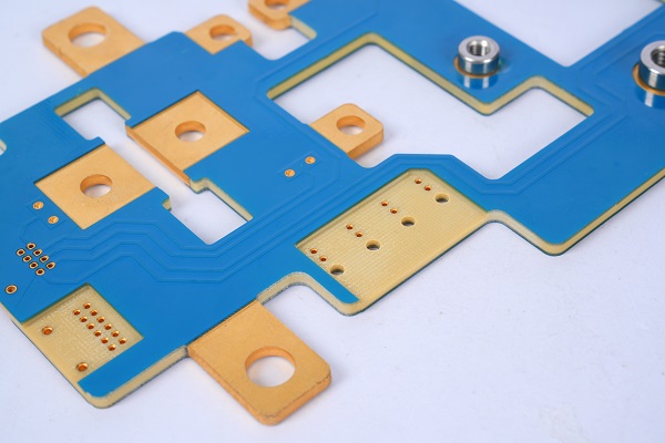
Applications of Heavy Copper PCBs
Heavy copper PCBs are used in a variety of applications, including:
- Power supplies
- Motor controllers
- Industrial machinery
- Automotive electronics
- Aerospace and defense systems
- Solar inverters
- LED lighting
Choosing the right PCB thickness is crucial for the success of any project. Heavy copper PCBs offer unique features and benefits that make them ideal for high-power and high-temperature applications. If you want to ensure the reliability and performance of your project, consider using heavy copper PCBs. EBest Circuit (Best Technology) has more than 16 years manufacturing experience in heavy copper PCBs, so we are so confident that we can be your most reliable supplier in China. Welcome to contact us at any time for any questions or any queries about PCBs.
You may also like


Tags: heavy copper pcb