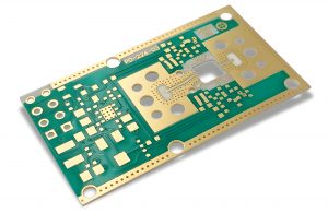
A high speed digital PCB depends on material loss, stackup control, impedance accuracy, clean routing, via structure, crosstalk control, reflection control and power integrity. These factors decide whether fast digital signals remain stable during prototype testing and mass production.
This guide explains practical design rules, layout checks, manufacturing controls, test methods and sourcing points for custom high-speed digital boards used in telecom, computing, industrial control, automotive electronics and IoT devices.
What Is a High Speed Digital PCB?
A high speed digital PCB is a circuit board where fast signal edges make traces behave like transmission lines. Trace width, spacing, dielectric thickness, copper roughness, via structure and reference planes all affect signal quality.
It is not defined only by clock frequency. A board may be high speed when rise time is short, data rate is high, or trace length becomes electrically significant. Common interfaces include USB, HDMI, Ethernet, PCIe, DDR, LVDS, MIPI and SerDes.
The core goal is stable timing, controlled impedance, clean waveform and low noise. Poor layout can cause ringing, crosstalk, EMI failure, random reset, unstable booting or communication errors.
Common applications include:
- Telecom routers, switches, gateways and 5G modules
- FPGA, processor and DDR memory boards
- Industrial control and robotics modules
- Automotive ADAS, infotainment and telematics boards
- Medical instruments and data acquisition systems
- AI edge computing and IoT gateway devices
How to Choose High Speed Digital PCB Materials?
Choose materials by data rate, trace length, loss budget, impedance target, temperature and cost. Standard FR-4 can support many moderate-speed designs. Long multi-gigabit channels usually require mid-loss or low-loss laminates.
Key material factors include Dk, Df, Tg, CTE, copper roughness, glass weave and dielectric thickness tolerance. For controlled impedance routing for high speed PCB projects, stable dielectric thickness and consistent Dk are essential.
| Material | Dk | Df | Tg | Typical Use |
|---|---|---|---|---|
| Standard FR-4 | 4.0–4.6 | 0.015–0.025 | 130–170°C | USB, Ethernet, MCU boards |
| High-Tg FR-4 | 3.8–4.4 | 0.012–0.020 | 170–180°C | Industrial digital boards |
| Mid-loss laminate | 3.4–3.8 | 0.006–0.012 | 170–200°C | PCIe, DDR, fast communication |
| Low-loss laminate | 3.0–3.6 | 0.002–0.006 | 180–220°C | SerDes and telecom boards |
| PTFE-based laminate | 2.1–3.2 | 0.0009–0.003 | 200°C+ | Very low-loss channels |
The right material is the lowest-risk laminate that meets signal loss, impedance and reliability targets. Do not select expensive materials blindly. Match the laminate to interface speed, channel length and production budget.
High Speed Digital PCB Stackup Design and Impedance Control
Stackup controls impedance, return path, EMI behavior, power distribution and batch consistency. Critical signal layers should stay close to solid ground planes or stable reference planes.
A good stackup keeps signal-reference coupling tight, avoids random plane splits, balances copper and supports impedance coupon testing. For dense BGA layouts, HDI stackup can reduce long breakout traces and unnecessary through vias.
| Layer Count | Common Structure | Typical Use | Impedance Target |
|---|---|---|---|
| 4L | Signal / GND / PWR / Signal | Simple high-speed modules | 50Ω, 90Ω, 100Ω |
| 6L | Signal / GND / Signal / PWR / GND / Signal | Ethernet, USB, compact controls | 50Ω, 90Ω, 100Ω |
| 8L | Signal / GND / Signal / PWR / GND / Signal / PWR / Signal | DDR, FPGA, processor boards | 40–60Ω, 85–100Ω |
| 10L+ | Multiple signal and plane pairs | PCIe, SerDes, telecom boards | Interface-specific |
Controlled impedance usually uses ±10% tolerance. Stricter designs may require ±5% tolerance after stackup approval, trace geometry review and impedance coupon confirmation.
Before layout release, confirm material type, dielectric thickness, copper weight, trace width, spacing, impedance target and coupon design with the PCB manufacturer.
High Speed Digital PCB Design Guidelines & Considerations
High speed digital PCB design should start from signal path planning, not from trace routing. A clean layout comes from correct placement, stackup, impedance, return path and power structure.
Step 1: Confirm interface requirements before layout.
List every high-speed interface, such as USB, Ethernet, PCIe, DDR, LVDS, MIPI or SerDes. Confirm impedance target, length matching rule, maximum trace length, reference layer and connector position before routing starts.
Step 2: Build the stackup with the PCB manufacturer.
Define layer count, dielectric thickness, copper weight and material type early. For controlled impedance routing for high speed PCB projects, stackup approval should happen before layout release, not after Gerber output.
Step 3: Place components by signal flow.
Put processor, memory, PHY, connector, clock and power circuits in a logical path. Shorter placement reduces trace length, via count, skew and routing congestion.
Step 4: Protect the return path.
Keep critical traces over solid reference planes. Avoid crossing split planes, voids, large cutouts or uncontrolled plane transitions. A broken return path can increase EMI, ringing and crosstalk.
Step 5: Route critical nets first.
Clock, DDR, differential pairs, SerDes and reset-sensitive nets should be routed before low-speed control signals. This keeps the most sensitive channels short, direct and clean.
Step 6: Review manufacturing and testing limits.
Check minimum trace width, spacing, via size, annular ring, impedance tolerance, solder mask clearance, BGA pitch and inspection method. A good design must match real PCB fabrication and assembly capability.
What Are the Best PCB Routing Rules for High Speed Digital Circuits?
High speed PCB routing rules should keep impedance stable, reduce noise and protect timing margin. The layout should make the signal path short, continuous and easy to manufacture.
- Keep critical traces short and direct.
Long traces increase loss, delay and noise exposure. Route clocks, DDR, PCIe, USB, Ethernet and other fast nets before low-speed signals. - Use continuous reference planes.
A high-speed signal should always have a nearby return path. Do not route critical traces across split planes, voids or large plane gaps. - Control trace width and spacing.
Follow the approved stackup and impedance table. Random neck-down areas can shift impedance and cause reflection. - Reduce unnecessary vias.
Each via adds inductance, capacitance and possible stub effects. Use layer changes only when they improve the total channel. - Separate noisy and sensitive nets.
Keep clocks, switching power nodes and high-current traces away from receivers, reset lines, analog circuits and crystal circuits. - Apply spacing rules by risk level.
Use 3W spacing for common high-speed separation and 5W or more for clocks, noisy buses or sensitive interfaces. - Avoid long parallel routing.
Long parallel sections increase crosstalk. If adjacent routing is unavoidable, increase spacing or shorten the parallel length. - Match length only where required.
Over-tuning can create extra coupling and impedance variation. Follow the datasheet instead of adding unnecessary serpentine traces.
How to Design Differential Pair Routing in High Speed PCB?
Differential pair routing in high speed PCB should keep two traces balanced from driver to receiver. Width, spacing, length, via transition and reference plane must stay consistent.
- Use the correct differential impedance.
Common targets are 85Ω, 90Ω or 100Ω, depending on the interface. PCIe, USB, Ethernet, HDMI, LVDS and MIPI should follow their own specification. - Keep both traces on the same layer.
Layer changes should be avoided where possible. If a transition is required, both lines should change layers together with symmetrical vias. - Keep spacing consistent.
Changing pair spacing changes differential impedance. Maintain the calculated gap from the approved stackup. - Control intra-pair skew.
Many designs use 5–10 mil as a practical target, but the device datasheet has priority. Skew should be corrected close to the mismatch point. - Avoid excessive serpentine tuning.
Long tuning patterns can add coupling and local impedance changes. Use short, smooth and compact tuning only when required. - Protect the reference plane.
The pair should not cross plane splits or voids. If the reference layer changes, add nearby ground stitching vias. - Keep pair-to-pair spacing larger.
Use 3W–5W spacing between different pairs to reduce crosstalk, especially near connectors and dense BGA areas.
What Via Design Rules Should Be Used in High Speed Digital PCB?
Via design for high speed digital PCB should reduce stub length, impedance discontinuity, insertion loss and return path interruption. In high-speed channels, a via is part of the signal path, not just a connection hole.
- Use fewer vias on critical signals.
Each via adds parasitic inductance and capacitance. Fewer transitions usually mean cleaner waveform and better signal margin. - Keep via transitions symmetrical.
For differential pairs, both traces should use the same via type, same layer transition and similar geometry. - Add nearby ground stitching vias.
When a high-speed signal changes layers, the return current also changes reference planes. Ground vias give return current a short path. - Reduce via stubs for fast channels.
Long through-hole stubs can cause reflection and resonance. Use blind vias, buried vias, microvias or back drilling when data rate and channel length justify the cost. - Confirm drilling and plating limits.
Check minimum via diameter, aspect ratio, annular ring, copper plating thickness and tolerance before layout release. - Use microvias carefully for fine-pitch BGA.
Microvias help escape dense devices, but reliability depends on stack structure, plating quality and lamination control. - Review via anti-pad design.
Anti-pad size affects impedance at the layer transition. For critical channels, the manufacturer should check via geometry together with the stackup.
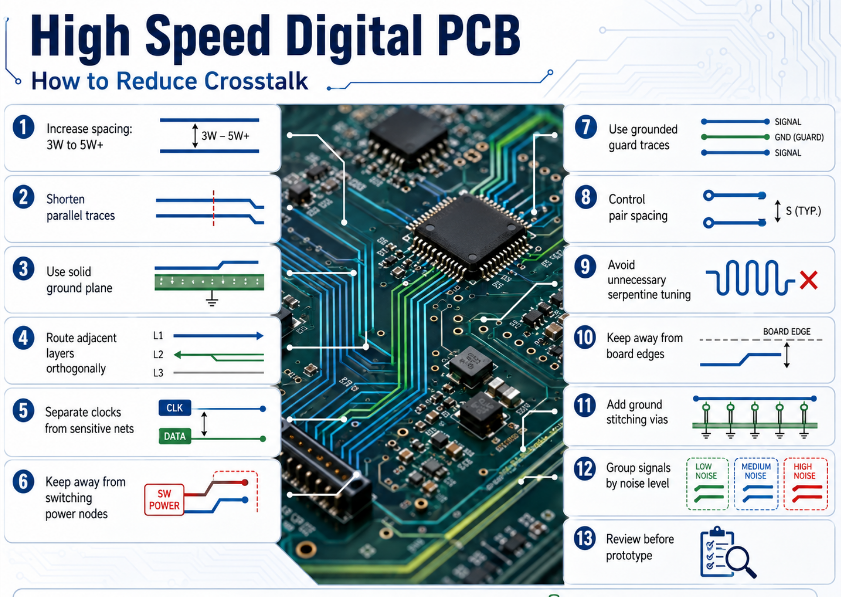
How to Reduce Crosstalk in High Speed Digital PCB?
Crosstalk in high speed digital PCB is reduced by controlling spacing, routing length, reference planes, signal grouping and return paths. The goal is to stop one fast signal from coupling noise into nearby traces.
- Increase spacing between high-speed traces.
Use 3W spacing as a common starting rule, where W is the trace width. For clocks, SerDes, DDR, reset lines or sensitive receiver signals, use 5W or more when board space allows. - Shorten parallel routing length.
Crosstalk becomes worse when two traces run side by side for a long distance. Keep parallel sections short, separate traces early and avoid long parallel routing near connectors, BGA escape areas and dense bus groups. - Keep a solid reference plane under critical traces.
High-speed signals should route over a continuous ground plane. Do not route them across split planes, voids, cutouts or changing reference areas. - Route adjacent signal layers in different directions.
If two high-speed routing layers are next to each other, route one layer horizontally and the other vertically where possible. This reduces broadside coupling between overlapping traces. - Separate clocks from data and control lines.
Clock signals switch continuously and can become strong noise sources. Keep clocks away from reset lines, interrupt lines, analog signals, crystal circuits and sensitive receiver inputs. - Avoid routing near switching power nodes.
Buck converter switch nodes, MOSFET gates, inductors and high-current pulse paths generate strong noise. Keep high-speed digital traces away from these areas. - Use ground shielding only when grounded correctly.
A guard trace can help in some layouts, but it must connect to ground with frequent stitching vias. A floating shield may increase coupling instead of reducing it. - Control differential pair spacing and pair-to-pair spacing.
Keep intra-pair spacing constant to maintain differential impedance. Increase spacing between different pairs, especially for PCIe, USB, Ethernet, HDMI, LVDS and MIPI interfaces. - Avoid unnecessary serpentine tuning.
Long serpentine traces can couple to themselves or nearby traces. Use compact tuning only where the interface requires length matching. - Keep high-speed traces away from board edges.
Traces near board edges can radiate more easily and may couple into cables, shields or nearby circuits. Keep critical clocks and fast buses away from edges when placement allows. - Use ground stitching vias near layer transitions.
When a high-speed signal changes layers, the return current also changes reference planes. Nearby ground stitching vias provide a shorter return path. - Group signals by speed and noise level.
Separate high-speed digital signals, low-speed control signals, analog signals and power switching circuits. Good grouping reduces routing conflict and unwanted coupling. - Check crosstalk before prototype release.
For dense BGA, DDR, SerDes or connector-heavy boards, review spacing, parallel length, layer order and reference planes before fabrication. Simulation is useful when signal margin is limited.
The practical rule is clear: keep fast traces spaced, short, well referenced and away from noisy circuits. For mass production, confirm stackup tolerance, trace spacing tolerance, connector breakout quality and impedance control with the PCB manufacturer.
How to Eliminate Signal Reflection in High Speed PCB?
Signal integrity in high speed digital PCB is improved by keeping impedance continuous from driver to receiver. Reflection happens when a fast signal meets sudden impedance change in the trace, via, connector or termination.
- Confirm controlled impedance before routing.
Use the manufacturer-approved stackup for trace width, spacing and dielectric thickness. Guessing trace width often creates mismatch. - Avoid long branches and T-routing.
Branches behave like stubs and reflect energy back into the main signal path. Use point-to-point routing where possible. - Control via stub length.
Through vias on thick boards can create unused barrel length. Back drilling or blind vias can reduce reflection in multi-gigabit channels. - Use correct termination.
Series, parallel or differential termination should follow the device datasheet. Wrong termination can cause overshoot, undershoot and ringing. - Keep connector transitions clean.
Connector footprint, breakout routing and reference plane design should be smooth. Poor transitions can close the eye diagram. - Avoid sudden geometry changes.
Sharp neck-down areas, large pad transitions and inconsistent spacing can shift impedance. Keep the channel geometry smooth. - Validate critical channels.
TDR, VNA, eye diagram or functional testing can confirm whether reflection is controlled after PCB fabrication and assembly.
How to Design Power Integrity (PI) and Decoupling Capacitor Placement?
Power integrity in high speed digital PCB keeps high-speed chips supplied with stable voltage during fast switching. Poor PI can cause jitter, reset, data errors, EMI problems and unstable communication.
- Place decoupling capacitors close to power pins.
High-frequency capacitors should be closest to the IC power and ground pins. The loop from capacitor to pin and back to ground must be short. - Use short and wide connections.
Narrow or long traces add inductance. Connect capacitors to planes with short traces and nearby vias. - Use proper capacitor value groups.
Common values include 0.01µF, 0.1µF, 1µF, 4.7µF, 10µF and 100µF, depending on chip current demand and regulator structure. - Keep power and ground planes tightly coupled.
Close plane spacing helps reduce power distribution impedance and improves high-frequency current delivery. - Place bulk capacitors near regulators and load groups.
Bulk capacitors support lower-frequency load changes. They should not replace small high-frequency capacitors near IC pins. - Avoid random capacitor stuffing.
More capacitors do not always improve PI. Wrong placement, high loop inductance or poor plane connection can reduce real effect. - Check regulator location and copper path.
High-current paths should be short and wide. FPGA, processor, DDR and communication chips should have enough copper area and vias. - Review thermal rise.
Power integrity and heat are connected. High current, thin copper and poor via design can increase voltage drop and temperature.
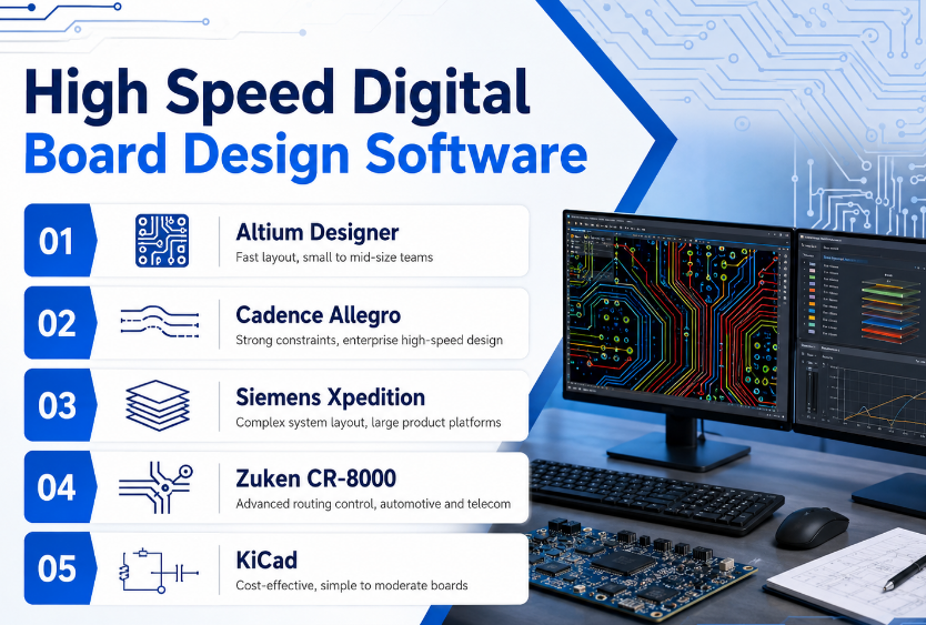
What PCB Design Software Is Best for High Speed Digital Board Design?
The best PCB design software should support constraint-driven layout, differential pair rules, length matching, impedance setup, stackup control and design rule checking.
| Software | Strength | Typical Fit |
|---|---|---|
| Altium Designer | Fast layout and usability | Small to mid-size teams |
| Cadence Allegro | Strong constraints and SI workflow | Enterprise high-speed design |
| Siemens Xpedition | Complex system layout | Large product platforms |
| Zuken CR-8000 | Advanced routing control | Automotive and telecom |
| KiCad | Cost-effective layout | Simple to moderate boards |
The tool should support net classes, differential pair setup, clearance rules, tuning rules, stackup manager, DRC and manufacturing output review.
Software alone does not guarantee performance. The layout rules must match real fabrication capability, material availability, impedance tolerance, assembly process and final test requirements.
FAQs About High Speed Digital PCB
Q1: When should a digital board be treated as a high speed digital PCB?
A1: A digital board should be treated as high speed when trace length becomes significant compared with signal rise time, or when interfaces such as PCIe, DDR, USB, Ethernet, HDMI, LVDS or SerDes are used. A fast edge at a lower frequency can still create transmission line behavior, reflection and EMI risk.
Q2: What should be checked during high speed digital PCB material selection?
A2: high speed digital PCB material selection should check Dk, Df, Tg, CTE, copper roughness, glass weave, dielectric thickness tolerance and laminate availability. For long multi-gigabit channels, lower Df and smoother copper can improve insertion loss and signal margin.
Q3: Why is high speed PCB stackup design important before routing?
A3: high speed PCB stackup design should be confirmed before routing because dielectric thickness, copper weight, reference plane location and material Dk directly affect impedance. Late stackup changes can force trace width changes, length adjustment and layout rework.
Q4: What impedance tolerance is common for high speed digital PCB manufacturing?
A4: Most controlled impedance boards use ±10% tolerance as a common production target. More demanding projects may request ±5% tolerance, but this requires tighter stackup control, stable material thickness, accurate etching and impedance coupon testing.
Q5: How does high speed digital PCB layout affect signal quality?
A5: high speed digital PCB layout affects signal quality through component placement, reference plane continuity, trace length, via count, pair spacing, crosstalk control and decoupling position. A clean layout reduces reflection, EMI risk and unstable communication.
Q6: Does solder mask affect high-speed trace impedance?
A6: Yes. Solder mask can slightly change impedance, especially on outer-layer microstrip traces. For tight impedance control, the PCB manufacturer should calculate final impedance with solder mask included, not only bare copper geometry.
Q7: Which surface finish is better for high speed digital PCB?
A7: ENIG is widely used because it provides good solderability, flat pads and stable assembly performance. OSP may reduce cost, while immersion silver may fit some high-frequency needs. The final choice should consider signal performance, shelf life, assembly method and reliability requirements.
Q8: Why do high-speed boards fail even when E-test passes?
A8: E-test checks open and short circuits, but it does not verify waveform quality, impedance continuity, crosstalk, reflection or power noise. Critical projects may require TDR, eye diagram, VNA, functional testing, X-ray inspection and thermal checks.
Q9: What is the role of TDR testing in high speed digital PCB?
A9: TDR testing measures impedance along a trace or coupon and shows where impedance changes occur. It helps verify whether the fabricated PCB matches targets such as 50Ω single-ended or 100Ω differential.
Q10: How does copper roughness affect signal integrity in high speed digital PCB?
A10: Copper roughness increases conductor loss at higher frequencies because current flows closer to the copper surface. For very fast interfaces, smoother copper and lower-loss materials can improve insertion loss, eye diagram performance and signal integrity in high speed digital PCB.
Q11: What are common digital high-speed PCB applications?
A11: Digital high-speed PCB applications include telecom modules, FPGA boards, DDR memory products, industrial controllers, AI edge devices, medical instruments and automotive communication boards. These products require stable impedance, clean routing and reliable power delivery.
Q12: Should all high-speed traces be length matched?
A12: No. Length matching should follow the interface requirement. DDR, differential pairs and some parallel buses need specific timing control, but unrelated high-speed traces do not need random matching. Excessive serpentine tuning can add coupling and impedance variation.
Q13: What design files help a manufacturer quote high speed digital PCB accurately?
A13: A complete package should include Gerber or ODB++ files, drill files, stackup, impedance table, material requirements, copper thickness, surface finish, solder mask color, BOM, pick-and-place file, assembly drawing, testing requirements and quantity. Clear targets such as 50Ω, 90Ω or 100Ω reduce quotation errors.
Conclusion
A high speed digital PCB succeeds when material, stackup, impedance, routing, via transition, return path, crosstalk control, reflection control, power integrity, fabrication, assembly and testing are managed as one system. For design selection, start with interface speed, trace length, impedance target, layer count, laminate loss and test requirements. This helps reduce redesign risk, improve signal stability and make prototype-to-mass-production transfer more reliable.
If you are looking for a China source factory for high speed PCB production and assembly, EBest can support custom high speed PCB fabrication, PCBA, DFM review, controlled impedance, HDI, BGA assembly, X-ray inspection, TDR testing, prototype builds and batch delivery. Send your Gerber files, BOM, stackup, impedance table and quantity to sales@bestpcbs.com for a fast quotation and practical engineering support.