PCB manufacturing PCB manufacturing
Home > Blog

How to Test Electronic Circuit Board?

January 2nd, 2026

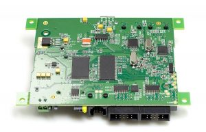
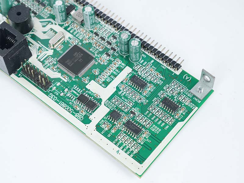
How to test electronic circuit board? Testing an electronic circuit board is a critical step to ensure functionality, reliability, and safety before mass production or deployment. A well-structured testing process helps identify design flaws, assembly defects, and component failures early—saving both time and cost.

How to Test Electronic Circuit Board?

How to Test an Electronic Circuit Board?

To begin, place the board on a stable surface with proper lighting. Before you touch anything, disconnect all power sources.

Next, perform a visual inspection. This simple act often reveals more information than expected. Look for burned areas, cracked components, lifted pads, poor solder joints, or debris. A magnifying lamp makes this process easier.

After the visual check, inspect connectors, jumpers, and wires. Loose connections appear harmless but often create intermittent issues that feel impossible to catch. A light touch with tweezers confirms stability.

Once the board passes the visual stage, move to electrical testing. A multimeter becomes your most trusted tool. Use continuity mode to confirm that important traces are connected. Use voltage mode to verify that power rails provide stable output. Use resistance mode to track suspicious paths.

During testing. If something feels unusual—temperature differences, unexpected noise, odd smells—pause and investigate.

By following these steps slowly and calmly, you can test an electronic circuit board with clarity and success.

How to Test Electronic Components on a Circuit Board?

Testing individual components is the next logical step because a PCB is only as reliable as each device mounted on it. When a component fails, it often takes down the entire function.

Start with passive components. Resistors are easy to check using the resistance mode on a multimeter. Measure across both ends. If the value appears close to the labeled rating, the resistor is healthy. If the value is extremely high, open, or inconsistent, it may be faulty.

Capacitors require a different approach. When testing capacitors, use capacitance mode if available. For electrolytic capacitors, check for bulging or leaking material. These symptoms almost always indicate failure. For ceramic capacitors, inspect for cracks. Even hairline cracks can cause unstable behavior.

Next, check diodes. These parts allow current to flow in only one direction. Use diode mode on your multimeter. A healthy diode shows one direction with low forward voltage and the other direction with high resistance. If it shows low resistance in both directions, it is bad.

Transistors require a bit more attention. You can test them using diode mode by checking junction behavior. If the readings do not follow expected patterns, the transistor may be damaged.

Integrated circuits are more complex to test directly. Instead, check their input and output voltages relative to the datasheet. If the IC receives the correct signals but responds incorrectly, it may be faulty.

Sensors, connectors, coils, and switches also deserve inspection. Loose contacts or internal breaks lead to intermittent failures that frustrate even experienced technicians.

How to Test Circuit for Short on Electronic Board?

A short circuit is one of the most common and stressful PCB issues. The good news is that detecting a short is often easier than expected, especially when using the right steps.

Begin by switching your multimeter to continuity mode. Touch one probe to the ground reference. Touch the other to various power points such as 3.3 V, 5 V, or 12 V rails. If you hear a beep, it means there is continuity—possibly a short.

Do not panic if continuity appears at first. Some circuits use intentional low-resistance paths. Instead, look for extremely low resistance, usually near zero ohms. That value often indicates a short.

Move through the board section by section. Check areas where power lines run close to ground. Solder bridges, damaged vias, and misaligned components cause accidental shorts more often than people realize.

If the PCB is multi-layer, you may need to isolate regions by lifting components such as decoupling capacitors. Removing them temporarily helps narrow down the exact node causing trouble.

Thermal cameras, even simple ones, can help detect shockingly fast where the short is hiding. Components sitting on a short path heat up quickly even with tiny amounts of voltage.

How to Test Electronic Circuit Board?

How to Test if a Circuit Board Is Bad?

  • First, observe the power behavior. If the board fails to start or shows unstable voltage, there may be a damaged regulator or short. Use your multimeter to check the rails. Healthy boards deliver stable readings.
  • Second, examine functionality. Does the board complete its tasks? Do LEDs light as expected? Does the CPU start? Even small symptoms provide big clues. For instance, an LED flickering instead of glowing steadily indicates unstable current or improper grounding.
  • Next, perform thermal observation. If any component heats too quickly, it may be failing. Healthy boards warm slowly and evenly.
  • Another sign is physical condition. Bad boards often exhibit damaged traces, cracked solder joints, corrosion, or burnt areas.

Software tools such as oscilloscopes or logic analyzers can also reveal deeper issues. Incorrect waveforms often indicate a bad board even when the components appear intact.

If several tests reveal inconsistent results, or if the board repeatedly fails under mild load, it is likely defective.

How Do I Test a PCB with a Multimeter?

A multimeter is one of the most powerful tools for testing PCBs because it reveals real electrical behavior.

To begin, ensure the multimeter battery is healthy. Weak multimeter power may give misleading readings.

Use the continuity mode to trace connections. This test is simple but effective because it verifies whether the PCB’s paths are intact. Place one probe on one end of a trace and the second at the opposite end. If the multimeter beeps, you confirm electrical continuity.

Use the resistance mode to examine suspicious components. High resistance where there should be low resistance is a warning.

How to Test Electronic Circuit Board?

Then use voltage mode on a powered board. Measure power rails to confirm stable output. Move on to test key IC pins. Compare the readings with datasheet requirements. Small deviations may indicate early failures. Larger gaps point to serious issues.

Finally, use current measurement if necessary. This test should be done carefully. Excess current flow usually points to a short or overheating component.

Can You Cut a Circuit Board and It Still Work?

The answer is: yes, a circuit board can still work after cutting, but only under specific conditions.

Cutting a PCB should be done with extreme care. The board will continue working only if you avoid damaging active traces, copper planes, or functional zones. Many PCBs contain dense routing, so a careless cut could destroy the device.

If you must cut a circuit board, examine the board layout first. Look for areas without copper. Many boards intentionally include cut-lines for modular use. These areas are safe to cut as long as you stay within the boundaries.

Use tools designed for PCB cutting such as scoring knives, mills, or board shears. Regular tools may crack the laminate or tear pads.

After cutting, inspect the edges. Smooth them if needed. Ensure no copper is exposed or touching unwanted surfaces.

When done properly, a cut PCB can continue working exactly as before. It depends entirely on how well you prepare and execute the cut.

How to Troubleshoot and Repair Electronic Circuit Boards?

Troubleshooting a PCB is a blend of logic, patience, and methodical thinking. The process begins with clear observation and continues through structured testing until the root problem is solved.

  • Start with the symptom list. What exactly is the board failing to do?
  • Next, examine power. In many cases, weak or unstable power is the hidden cause behind strange behavior.
  • Move on to signal behavior. Use tools like oscilloscopes or logic probes to check timing and waveform integrity. Unexpected waveforms often signal failing components or broken connections.
  • Then follow a zone-based approach. Break the board into functional regions—power, processing, communication, outputs, and sensors. If you suspect a component, replace one part at a time. Do not replace everything at once.
  • Reflowing solder joints also saves many boards. Cold joints and cracked pads create intermittent issues that vanish after a clean reflow.

With these methods, troubleshooting and repairing electronic circuit boards will become a predictable process.

How to Test Electronic Circuit Board?

Conclusion:

Whether you are checking components, detecting shorts, verifying power rails, testing the board with a multimeter, cutting a PCB safely, or repairing complex circuits, the process becomes manageable when broken into structured steps.

If you need assistance with PCB design, manufacturing, or troubleshooting support, feel free to contact us at sales@bestpcbs.com

You may also like

Trusted Medical PCB Assembly Services for Modern Healthcare

January 2nd, 2026

Medical PCB assembly services​ are the specialized production and system integration of printed circuit boards for life-critical medical equipment. This article explores how partnering with the right provider ensures reliability, compliance, and innovation in healthcare technology.

Developing a new medical device is a high-stakes endeavor. Key Pain Points for Medical Device Developers:

  • Regulatory Maze:​ Navigating FDA, ISO 13485, and IEC 60601 standards without expert guidance is time-consuming and risky.
  • Design for Manufacturing (DFM) Gaps:​ Prototype designs often have hidden flaws that cause failures during volume production.
  • Supply Chain Insecurity:​ Unreliable component sourcing or offshore delays jeopardize project timelines and device availability.
  • Inconsistent Quality:​ Lack of rigorous process controls leads to field failures, recalls, and patient safety risks.
  • Prototype Bottlenecks:​ Slow turnaround times for design iterations critically delay testing, verification, and time-to-market.

These challenges demand a partner with specialized expertise. The following solutions are foundational to a trusted medical electronics manufacturing relationship.

  • Proactive Compliance Framework:​ A partner with ingrained quality systems (ISO 13485 certified) guides you through documentation and validation seamlessly.
  • Early DFM/DFA Analysis:​ Expert engineers review designs pre-production to eliminate errors, enhance reliability, and reduce costs.
  • Controlled, Traceable Supply Chain:​ Using a vetted network of component suppliers and US based PCB assembly​ capabilities mitigates shortage and geopolitical risks.
  • Robust Quality & Testing Regime:​ Implementing automated optical inspection (AOI), X-ray, and functional testing ensures every board meets stringent medical-grade specifications.
  • Dedicated Rapid Prototyping Lines:​ Offering quick turn PCB USA​ services accelerates the design-test-iterate cycle, getting you to clinical trials faster.

EBest Circuit (Best Technology) is a specialized PCB manufacturing and assembly provider focused on the rigorous demands of the medical sector. Our state-of-the-art facility is ISO 13485:2016 certified, and our global production network includes advanced SMT factories in both China and Vietnam. Each site operates under a unified MES-driven manufacturing system, enabling full process traceability, tighter quality control, and consistent performance across all medical projects. Our engineering team is dedicated to merging technical excellence with regulatory mastery, ensuring every medical PCB meets the highest reliability and compliance standards. For a consultation on your next PCBA printed circuit board assembly project, contact us at sales@bestpcbs.com.

Medical PCB Assembly Services

How Do Medical PCB Assembly Services Ensure Reliable Performance in Today’s Healthcare Electronics?

Reliable performance in medical electronics is non-negotiable. Medical PCB assembly services​ achieve this by implementing a multi-layered approach to quality and control that far exceeds commercial standards.

  • Medical-Grade Materials & Components:​ Only using high-Tg laminates, conformal coatings, and components rated for extended life and stable performance in physiological environments.
  • Enhanced Process Controls:​ Strict adherence to controlled procedures for soldering (e.g., lead-free SAC305 profiles), cleanliness (ionic contamination testing), and electrostatic discharge (ESD) protection.
  • Comprehensive Testing Protocol:​ Every board undergoes a battery of tests:
Test MethodPurpose
Automated Optical Inspection (AOI)Catches soldering defects, missing, or misaligned components.
X-Ray InspectionVerifies integrity of BGAs, internal layers, and via fills.
In-Circuit Test (ICT)Checks electrical performance and component values.
Functional Test (FVT)Simulates the device’s real-world operation.
  • Full Traceability:​ Lot-by-lot and even board-level tracking of all materials and components is maintained, a critical requirement for FDA audits and potential recall actions.
  • Environmental Stress Screening (ESS):​ Subjecting boards to thermal cycling and burn-in to identify and eliminate early-life failures (infant mortality).

In summary, reliability is engineered through a combination of superior materials, meticulous processes, and exhaustive verification, ensuring devices perform as intended over their entire service life.

Medical PCB Assembly Services

What Is the Difference Between PCB Fab and Assembly?

The journey from design to a functional board involves two distinct, sequential phases: fabrication (PCB fab) and assembly (PCB manufacturing and assembly). Confusing them can lead to project missteps.

  • PCB Fabrication (Fab):​ This is the process of manufacturing the bare, unpopulated circuit board. It starts with design files (Gerbers) and involves:
    • Creating the substrate laminate.
    • Imaging and etching the copper layers to form traces.
    • Drilling holes (vias and through-holes).
    • Applying solder mask and silkscreen.
    • Performing electrical testing on the bare board.
    • Output:​ A bare PCB with pads and holes, ready for components.
  • PCB Assembly (PCBA):​ This is the process of mounting and soldering electronic components onto the fabricated bare board. It involves:
    • Applying solder paste via stencil.
    • Placing components (Surface-Mount Technology – SMT) using pick-and-place machines.
    • Reflow soldering to create electrical connections.
    • Through-hole component insertion and soldering.
    • Cleaning, inspection, and functional testing.
    • Output:​ A fully functional, populated printed circuit board assembly.

Think of PCB fab​ as printing the wiring diagram and PCB assembly​ as installing all the light switches, outlets, and fixtures. A true turnkey partner, like a professional PCB design company​ turned manufacturer, expertly manages both phases.

Why Medical PCB Assembly Services Demand Higher Standards Than Conventional PCB Manufacturing and Assembly?

Medical devices directly impact human life, making failure unacceptable. This fundamental truth elevates every requirement from the component level to the final system integration.

  • Regulatory Scrutiny:​ Medical devices require formal approval (FDA, CE). The entire production process must be documented and validated under standards like ISO 13485. A simple process change in conventional manufacturing can become a major, documented change request in medical.
  • Extreme Reliability & Longevity:​ A consumer device may have a 2-3 year life. An implantable or critical care device must function flawlessly for 10-15+ years. This demands higher-grade materials and accelerated life testing.
  • Risk Management (ISO 14971):​ Every potential failure mode must be identified, analyzed, and controlled. The assembly process itself is a critical control point to mitigate risks like short circuits or cold solder joints.
  • Biocompatibility & Cleanliness:​ Devices contacting patients must not leach harmful substances. Assembly processes must ensure extreme cleanliness to avoid ionic contamination that could cause corrosion or failure.
  • Traceability:​ While batch traceability might suffice for consumer goods, medical devices often require component-level traceability to facilitate targeted recalls if a supplier’s component batch is found faulty.

Therefore, medical PCB assembly services​ are not just about soldering components; they are about executing a rigorously controlled, documented, and validated protocol where quality is measured in patient safety outcomes.

How Best Rigid-Flex PCB Assembly Services for Medical Devices Enhance Durability and Miniaturization?

Best rigid-flex pcb assembly services for medical devices​ unlock innovative form factors by combining rigid boards for component support with flexible circuits for dynamic movement and space savings.

  • Enhancing Durability:
    • Reduced Interconnections:​ Replacing fragile connectors and ribbon cables with soldered flex connections minimizes points of failure.
    • Vibration/Shock Resistance:​ The flexible portions absorb and dissipate mechanical stress, protecting solder joints.
    • Improved Reliability:​ A monolithic rigid-flex structure is more reliable than an assembly of multiple interconnected rigid boards.
  • Enabling Miniaturization & Wearability:
    • 3D Packaging:​ Boards can be folded into compact, three-dimensional shapes, crucial for implants, hearing aids, and endoscopic capsules.
    • Weight Reduction:​ Eliminating connectors and using thin flex layers reduces overall weight—key for portable and wearable monitors.
    • Dynamic Flexing:​ Allows for designs in hinged devices or probes that require repeated movement.

For a factory wholesale medical PCB assembly service, mastering rigid-flex is a key capability. It requires specialized PCB fab​ expertise for multilayer bonding and precise PCB assembly​ techniques to handle the delicate flex areas during soldering and handling.

Capabilities of a US Based PCB Assembly Partner for Healthcare OEMs

A US based PCB assembly partner provides a mature infrastructure, advanced engineering support, and tightly controlled manufacturing systems tailored for the demanding needs of Healthcare OEMs.

Advanced Engineering Collaboration
Localized teams provide rapid design reviews, DFM/DFA optimization, and direct engineering communication that shortens development cycles and reduces risk before prototypes are built.

Highly Controlled Manufacturing Processes
U.S. facilities apply strict process validation, IPC Class 3 manufacturing, real-time monitoring, and data-driven production oversight aligned with FDA and ISO 13485 expectations.

Robust Traceability and Documentation Systems
MES-based traceability, controlled documentation, and production records tailored for medical audits support DHF/DMR requirements and simplify compliance workflows.

Reliable Quick-Turn Prototyping and Small-Batch Production
Domestic fabrication and assembly resources enable consistent quick turn PCB USA results, accelerating verification testing and early clinical evaluations.

Secure and Verified Supply Chain
U.S. partners maintain qualified suppliers, validated sourcing protocols, and controlled inventory management to support long-term availability and stable BOM planning.

Specialized Medical Manufacturing Expertise
Experienced operators, medically trained technicians, and quality teams understand the expectations of Healthcare OEMs—from cleanliness requirements to test coverage and failure analysis.

A US based PCB assembly partner is not merely a vendor—it is a capability-driven extension of your R&D and manufacturing team, providing the technical depth, control, and confidence required for regulated medical devices.

How a Professional PCB Design Company Supports Medical Product Development from Concept to Verification?

A professional PCB design company​ is a vital co-pilot, transforming a conceptual medical device into a manufacturable, reliable, and certifiable product.

  • Concept & Architecture:​ Advises on system partitioning, component selection, and technology (e.g., rigid-flex) to meet size, power, and cost targets.
  • Schematic Capture & Simulation:​ Creates the electrical blueprint and runs signal/power integrity simulations to prevent performance issues.
  • PCB Layout with DFM/DFA Rules:​ Engineers the physical board layout with strict adherence to medical-grade spacing, high-reliability routing, and, crucially, Design for Manufacturing/Assembly​ rules from the start.
  • Design for Test (DFT):​ Incorporates test points and features to ensure the assembled board can be thoroughly validated.
  • Documentation for Compliance:​ Generates the complete design history file (DHF) output needed for regulatory submission, including schematics, layouts, BOMs, and design rationale.
  • Support through Verification & Validation (V&V):​ Works with the assembly partner to troubleshoot prototype builds and provide design revisions.

This end-to-end support de-risks development, ensuring the design is optimized not just for function, but for manufacturability and compliance from day one.

Why Many Healthcare Startups Seek Quick Turn PCB USA Solutions for Prototype Acceleration?

For healthcare startups, speed to proof-of-concept and clinical validation is critical for funding and market entry. Quick turn PCB USA​ services are the engine for this acceleration.

  • Rapid Design Iteration:​ Fast prototype turns (e.g., 24-72 hours for fab, 5-10 days for assembly) allow engineers to test, discover flaws, and refine designs in quick succession.
  • Faster Clinical & Regulatory Milestones:​ Functional prototypes are needed for benchtop testing, animal studies, and human trials. Faster builds compress the overall development timeline.
  • Cost-Effective Exploration:​ Enables affordable testing of multiple design approaches or form factors before locking in final tooling for volume production.
  • Attracting Investment:​ A working, refined prototype is far more compelling to investors than just a CAD model or idea.

By leveraging domestic quick turn PCB USA capabilities, startups maintain agility and momentum, turning innovative ideas into tangible devices with exceptional speed.

How Can a Factory Wholesale Medical PCB Assembly Service Ensure Consistent Quality and Compliance for Regulated Healthcare Devices?

A true factory wholesale medical PCB assembly service​ achieves consistent quality not through luck, but through a systemic, process-oriented approach built for the medical industry.

  • Certified Quality Management System (QMS):​ Operation under ISO 13485:2016 is not optional; it’s the foundational framework that ensures consistent processes, corrective actions, and management oversight.
  • Standardized Work Instructions & Process Validation:​ Every assembly step is defined, documented, and validated to prove it consistently produces a result meeting pre-defined specifications.
  • Advanced Process Control & Monitoring:​ Solder paste inspection (SPI), automated optical inspection (AOI), and real-time thermal profiling of reflow ovens catch deviations in real-time.
  • Rigorous Supplier Management:​ Components are sourced from approved vendors with full lot traceability. Incoming materials are inspected and certified.
  • Independent Quality Assurance:​ A dedicated QA team, separate from production, performs audits and final releases based on data, not production schedules.
  • Continuous Training:​ Personnel are regularly trained on medical device regulations, soldering standards (IPC-A-610 Class 3), and cleanroom protocols.

This holistic system transforms a factory wholesale​ operation from a cost center into a reliable, compliance-driven partner for regulated device manufacturing.

Why Partnering With a PCB Design Company Is Essential for Creating Safe and Reliable Medical Electronics?

Partnering with a PCB design company​ with medical expertise is essential because safety and reliability are designed in, not tested in. They bridge the gap between brilliant medical innovation and real-world, manufacturable hardware.

  • Risk Mitigation by Design:​ Experts incorporate safety standards (like IEC 60601 for isolation and leakage currents) directly into the schematic and layout, designing out potential electrical hazards.
  • Designing for Long-Term Reliability:​ They understand and design for factors like thermal management, signal integrity in noisy environments, and mechanical stress—all critical for devices that must work for years without fail.
  • Avoiding Costly Late-Stage Re-Spins:​ Early DFM/DFA analysis prevents fundamental flaws that would require a complete board redesign after tooling is set, saving immense time and cost.
  • Navigating Regulatory Documentation:​ Their deliverables become a core part of the technical file required for regulatory submission, ensuring the design is presented correctly to auditors.

Ultimately, this partnership ensures the electronic foundation of your medical device is as innovative, safe, and robust as the medical concept itself.

Medical PCB Assembly Services

To sum up, medical PCB assembly services​ form the critical, reliable backbone of modern healthcare electronics, from life-sustaining implants to diagnostic equipment. This article has detailed how specialized expertise in design, fabrication, assembly, and testing converges to meet the unparalleled standards of the medical field.

Choosing a partner with deep medical market experience, robust quality systems, and a collaborative approach is not just a procurement decision—it’s a strategic investment in your product’s success and patient safety. As an ISO 13485:2016 certified specialist in medical PCB assembly services, EBest Circuit (Best Technology)​ combines engineering precision with regulatory insight to guide your device from prototype to volume production with unwavering quality. For more information or if you would like to send us any inquiry, please send us an email through the contact form at the bottom of our Contact Page.

You may also like

Which Lead Free Solder Material is Best for PCB Assembly?

December 31st, 2025

As global electronics manufacturing moves away from hazardous substances, lead free solder material has become the industry standard for PCB assembly. Driven by regulations such as RoHS and REACH, lead-free solder is now used in consumer electronics, automotive PCBs, industrial control boards, and medical devices.

However, not all lead-free solder materials are the same. Their composition, melting temperature, mechanical strength, and reliability vary significantly—making material selection critical for high-quality PCB assembly.

This guide explains what lead-free solder is, its composition, properties, types, melting temperatures, common soldering issues, and finally answers the key question: “Which lead free solder material is best for PCB assembly?”

What Is Lead Free Solder Material?

Lead free solder material is a metallic alloy used to join components to a PCB without the use of lead. Traditional solder contained 40% lead (Sn60/Pb40) or 37% lead (Sn63/Pb37). These alloys were easy to use but posed environmental and health concerns. Today, electronics manufacturers worldwide use lead-free formulations based on tin, silver, copper, bismuth, nickel, or small alloying elements.

From a customer’s perspective, lead free solder material is important because it directly affects:

  • Solder joint strength
  • Heat tolerance
  • Long-term reliability
  • Appearance of solder joints
  • Compatibility with high-density SMT packages
  • Product compliance with RoHS, REACH, and WEEE regulations

Lead-free solder also withstands higher temperatures, which is critical for modern high-density PCBs.

Which Lead Free Solder Material is Best for PCB Assembly?

Is Lead-Free Solder Still Toxic?

Lead-free solder eliminates lead—a major toxic substance—but that does not mean every alloy is completely risk-free. For normal PCB manufacturing environments, lead-free solder is considered safe and non-toxic when handled properly.

From a customer standpoint:

  • Lead-free solder is significantly safer than leaded solder
  • It does not release toxic lead fumes during reflow
  • Flux fumes—not the solder—are usually the irritation source
  • Lead-free waste requires less strict disposal procedures

Most concerns come from misunderstanding. Lead-free alloys like SAC305 (Sn96.5 Ag3.0 Cu0.5) are not harmful under standard handling and reflow conditions. With adequate ventilation and proper gloves, operators face minimal exposure risks.

Lead Free Solder Material Composition

Lead-free solder material compositions vary depending on cost targets, performance needs, and thermal sensitivity of the PCB. Below is a customer-friendly comparison of common alloys:

Common lead-free soldering compositions

Alloy TypeCompositionCharacteristicsBest Use
SAC305Sn96.5 / Ag3.0 / Cu0.5Most popular global alloy; balanced cost and performanceSMT reflow, general assembly
SAC405Sn95.5 / Ag4.0 / Cu0.5Higher silver for stronger joints and better wettingAutomotive, medical, mission-critical devices
SAC0307Sn99 / Ag0.3 / Cu0.7Cost-effective low-silver alternativeConsumer electronics, cost-controlled projects
Sn99.3Cu0.7Tin/copper mixSlightly higher melting point; durable in wave solderingWave solder baths
Sn-Bi alloysTin + Bismuth blendsLow melting point; ideal for heat-sensitive substratesLED boards, flex circuits, thin PCBs
Sn-Ag alloysTin + SilverGood wetting and moderate melting rangeFine-pitch soldering
Ni-doped SACSAC + NiImproved grain refinementAutomotive, aerospace

For most consumer and industrial applications, SAC305 is the ideal balance of performance and cost. Customers requiring high-temperature reliability (automotive, aerospace, telecom) may consider doped SAC alloys.

Lead Free Solder Material Properties

Lead-free solder is a low-lead soldering material based mainly on tin-based alloys such as Sn-Ag-Cu, Sn-Cu, and Sn-Bi. It is designed to replace traditional Sn-Pb solder and meet environmental regulations such as RoHS while reducing heavy-metal pollution. It’s properties can be explained from different aspects:

1. Physical & Process Characteristics

  • Melting Range: Wide, typically 138°C–250°C depending on alloy. SAC305 melts around 217°C. Most alloys have a narrow solid–liquid range for stable soldering.
  • Wetting: Good wetting behavior during reflow (30–90 seconds above liquidus) and wave soldering (≈4 seconds contact), forming reliable joints.
  • Conductivity: Electrical conductivity around ≄9.5×10⁶ S/m and thermal conductivity near 66 W/m·K, similar to Sn-Pb alloys.
  • Oxidation & Flow: Strong anti-oxidation and smooth flow with low dross generation, reducing defects such as bridging and solder spikes.

2. Mechanical Performance

  • Strength & Fatigue: Mechanical strength and fatigue life can be optimized through alloy design. Sn-Ag-Cu systems (e.g., 95.4Sn/3.1Ag/1.5Cu) offer strength comparable to or better than Sn-Pb.
  • Brittleness: Higher Ag or Cu content may reduce ductility, so alloy balance is important.
  • Reliability: Lead-free joints maintain stability under vibration and thermal cycling, suitable for harsh applications like automotive electronics.

3. Environmental & Cost Characteristics

  • Compliance: Lead content is typically below 1000 ppm, fully RoHS-compliant and safer for workers and the environment.
  • Cost: Generally 2–3× higher than traditional solder due to tin and silver pricing, but the impact on total product cost is usually limited.

4. Application & Compatibility

Lead-free solder is widely used in consumer electronics, automotive systems, medical devices, and new-energy applications. It works with standard fluxes and existing equipment such as 8-zone reflow ovens, though reflow profiles and process parameters may require adjustment to accommodate higher melting temperatures.

Types of Lead Free Soldering Method

Lead-free soldering involves several manufacturing methods designed around different processes, temperature profiles, and assembly requirements. When customers review PCB assembly quotes, the type of soldering used has a major impact on product durability, electrical integrity, and cost. Below are the core types of lead free soldering used in modern electronics production.

1. Lead-Free Reflow Soldering (SMT Reflow)

This is the most common method for mounting surface-mount components (SMDs). Manufacturers print lead-free solder paste onto pads, place components via pick-and-place machines, and heat the PCB in a controlled reflow oven. Reflow soldering has many advantages:

  • Suitable for nearly all SMT components
  • Works with SAC305, SAC405, SAC0307, and Sn-Bi pastes
  • Ensures consistent joint quality in mass production
  • Supports fine-pitch ICs, BGA, QFN, 0201/01005 components

Typical reflow peak temperature

  • 235–250°C, depending on the alloy and PCB materials

Reflow soldering is the backbone of every modern SMT line and the main reason SAC305 is widely used.

Types of Lead Free Soldering Method

2. Lead-Free Wave Soldering

Wave soldering is used primarily for through-hole components and mixed-technology assemblies.

During lead-free wave soldering, the PCB passes over a molten solder “wave” typically made of Sn99.3Cu0.7 or other tin-rich alloys.

Why customers care:

  • Ideal for high-volume assemblies with many through-hole connectors
  • Faster than hand soldering
  • Strong, uniform joints across large PCBs
  • But requires strict temperature control due to higher melting points

Common lead-free wave solder alloy

  • Sn99.3/Cu0.7, with optional micro-alloying (Ni, Ge) to reduce copper dissolution

Typical pot temperature

  • 255–265°C, depending on alloy
Lead-Free Wave Soldering

3. Lead-Free Selective Soldering

Selective soldering is used when only certain through-hole components must be soldered without exposing the entire PCB to a wave. A programmable nozzle creates localized molten solder “mini waves.”

Why customers care:

  • Protects heat-sensitive components
  • Reduces overall thermal stress
  • Useful for complex PCBs with dense SMT areas
  • Generates precise and stable joints

Common alloys

  • Sn99.3Cu0.7
  • SAC variants for specialized cases

Selective soldering is popular in industrial controllers, automotive electronics, and telecom boards.

Lead-Free Selective Soldering

4. Lead-Free Hand Soldering

Used for repair, prototyping, or small-batch assembly. Technicians use solder wire (typically SAC305 or SAC0307) and temperature-controlled irons.

Why customers care:

  • Required for last-minute rework
  • Used in prototype and engineering samples
  • Easy way to repair or modify boards
  • Quality depends heavily on operator skill and iron temperature

Hand soldering temperature

  • 350–380°C for SAC alloys
  • 280–310°C for Sn-Bi low-temp solder
Lead-Free Hand Soldering

Here is a quick comparison between these lead-free solder material methods:

Soldering TypeMain FeaturesTypical AlloysCustomer Use Case
Reflow SolderingStandard SMT processSAC305, SAC0307Consumer & industrial electronics
Wave SolderingHigh-volume through-holeSn99.3Cu0.7Power boards, large PCBs
Selective SolderingLocalized solderingSn-Cu, SACMixed-technology PCBs
Hand SolderingRework / prototypingSAC305 wireEngineering builds, repairs

Does 60/40 Solder Contain Lead?

Yes, 60/40 solder (Sn60/Pb40) contains 40% lead, so it is not RoHS compliant and must not be used in modern commercial electronics.

Lead-free solder materials replace this alloy entirely in global manufacturing unless exemptions apply (e.g., military or aerospace exceptions).

Lead-Free Solder Melting Temperature Chart

Below is a melting temperature chart customers can use as a reference during material selection or reflow profile planning:

Lead-Free AlloyMelting Temperature (°C)Notes
SAC305217–220°CMost common for SMT
SAC405217–225°CHigher Ag content improves strength
SAC0307~227°CBudget option; slightly higher melting point
Sn99.3Cu0.7227°CIdeal for wave soldering
Sn-Bi138–170°CBest for low-temp applications
Sn63/Pb37 (leaded)183°CFor comparison only

Customers should always verify that their components can tolerate the peak reflow temperature required by the alloy.

What Are the Main Issues With Lead-Free Soldering?

Lead-free soldering is reliable, but it requires proper process control. Common challenges include:

  • Higher melting point that stresses components
  • Slower wetting that demands optimized flux
  • Sometimes duller appearance of joints
  • Increased copper dissolution in wave soldering
  • Sensitivity to reflow temperature deviations

Why Is My Lead-Free Solder Not Melting?

Typical causes include:

  1. Iron or reflow temperature not high enough.
  2. Insufficient heat transfer due to oxidation or contamination.
  3. Using a low-power soldering iron unable to maintain temperature.
  4. Weak flux activity preventing proper heat flow.
  5. Applying the solder to a large thermal pad without preheating.

Lead-free solder requires around 30–40°C higher heat than leaded solder.

Which Lead Free Solder Material Is Best for PCB Assembly?

For most customers, SAC305 (Sn96.5/Ag3.0/Cu0.5) is the best lead-free solder material for PCB assembly.

Why SAC305 Is Ideal for Most Applications?

  • Widely used across global SMT factories
  • Excellent wetting on FR4, HDI, flexible, and ceramic substrates
  • Strong mechanical performance
  • Good thermal cycling reliability
  • Low voiding rate with proper reflow control
  • Compatible with nearly all flux chemistries
  • Proven in millions of consumer and industrial electronics

When Other Alloys Might Be Better?

  • SAC0307 – When cost is the priority
  • Sn-Bi – For low-temperature PCBs and LED products
  • SAC405 – For high-reliability automotive or medical electronics
  • Sn99.3Cu0.7 – For wave soldering to reduce cost

Customer Recommendation

If you are unsure which alloy to choose, start with SAC305 for standard SMT reflow because it aligns with:

  • Reliability expectations
  • Cost targets
  • Compatibility with modern assembly lines
  • Strong field performance

FAQs

1. What is the most common lead-free solder in SMT assembly?

SAC305 is the industry standard for most SMT production lines.

2. Is lead-free solder as strong as leaded solder?

Yes. Lead-free joints are typically stronger in mechanical strength and thermal fatigue resistance.

3. Why is lead-free solder harder to work with manually?

It melts at a higher temperature and wets more slowly, requiring better temperature control.

4. What flux should be used with lead-free solder?

Most solder pastes use no-clean or water-soluble fluxes optimized for SAC alloys.

5. Can lead-free solder be used with ENIG finish?

Yes, ENIG is one of the best surface finishes for consistent wetting.

You may also like

OEM vs ODM in PCB Manufacturing & How to Choose?

December 27th, 2025

Choosing the right manufacturing model is one of the most important strategic decisions for electronics companies. In the PCB and PCBA sector, product lifecycles are shorter, technical requirements are higher, and global competition is stronger than ever. In this environment, two models, OEM and ODM, shape how your boards move from idea to mass production.

This guide explains both models in clear terms, compares them using real PCB scenarios, and provides a practical decision framework that engineers, buyers, and founders can use when planning their next PCB or PCBA project.

OEM vs ODM in PCB Manufacturing & How to Choose?

What Is OEM Manufacturing in the PCB Industry?

OEM manufacturing refers to a model where the customer owns the product design, controls the technical specifications, and provides the documentation needed for production. In the PCB field, an OEM project usually includes:

  • Complete Gerber files and drill files
  • Stack-up information and layer count definition
  • Bill of materials (BOM) with approved vendor list
  • Assembly drawings and mechanical constraints
  • Testing procedures and acceptance criteria
  • Quality and reliability requirements

Under the OEM model, the PCB manufacturer acts as a specialist executor. The factory fabricates boards,
assembles components, and runs tests in strict alignment with the customer’s design and documentation.

The engineering ownership remains on the customer side, while the manufacturer delivers robust production, process control, and supply chain support.

In the PCB industry, OEM manufacturing is common in fields where design control and traceability matter:

  • Medical instrumentation and life-support electronics
  • Automotive electronics and ADAS-related boards
  • Aerospace and defense control modules
  • High-frequency RF and microwave PCBs
  • Industrial automation controllers
  • Robotics and motion control systems

These applications often involve tight regulations, proprietary algorithms, and long-term maintenance. Companies choose the OEM path because it allows them to keep full control of their PCB design while relying on an experienced manufacturing partner for fabrication, assembly, and testing.

What Is ODM Manufacturing in the PCB Industry?

ODM manufacturing goes beyond production and includes design and development. Instead of providing a finished design, the customer shares functional requirements, performance targets, and budget expectations. The ODM manufacturer then handles engineering and turns the requirements into a manufacturable PCB or PCBA solution.

Typical ODM services in the PCB domain include:

  • Circuit concept and schematic design
  • PCB layout and stack-up planning
  • Component selection and alternative sourcing
  • Design for manufacturability (DFM) and design for assembly (DFA)
  • Prototype build and design iterations
  • Compliance support and basic certification guidance
  • Full-scale production and functional testing

Many growing electronics brands, start-ups, and non-technical founders choose ODM when they need a finished PCB solution but do not have sufficient internal engineering resources. The manufacturer becomes both a design partner and a production partner.

In the PCB and PCBA world, ODM is frequently used for:

  • IoT sensor nodes and gateways
  • Smart home and building automation devices
  • Wearable electronics and fitness trackers
  • LED lighting drivers and control boards
  • Consumer electronics modules and controller boards
  • Low-power wireless communication boards

These market segments evolve quickly and demand frequent updates. A capable ODM PCB partner can speed up development and help clients get new boards into the market much faster.

OEM vs ODM: Core Differences for PCB and PCBA Projects

Both OEM and ODM are valuable, but they solve different problems. Understanding how they
differ helps you select the model that fits your product, budget, and timeline.

AreaOEMODM
Design OwnershipCustomer owns design, files, and IPManufacturer often owns design unless transferred by contract
Development CostLower upfront design cost, higher internal engineering investmentHigher upfront design charge, reduced internal engineering load
Time to MarketDepends on customer’s design speedShorter due to in-house design resources and templates
Engineering SupportFocused on DFM, DFA, and production adviceFull design plus optimization support
MOQ FlexibilityOften higher for mature productsCan be lower for pilot and first launches
Customization LevelUnlimited customization within process capabilityOften based on existing platforms or reference designs
IP ProtectionVery strong, assuming secure data handlingContract-dependent; must be clearly defined
Risk ProfileLower in production, higher in internal design qualityLower design risk, but higher IP and dependency risk

Engineers often pick the OEM route when they need tight control over design, especially for high-end or
regulated PCBs. Teams that prioritize speed, flexibility, and reduced internal workload tend to lean toward ODM.

When Should a PCB Company Choose OEM?

The OEM manufacturing model is ideal when technical control, long-term stability, and full customization
are your highest priorities.

You should prefer OEM when:

  • You already have a PCB design or a strong internal R&D and layout team.
  • Your product must comply with strict standards such as ISO 13485, IATF 16949, or specific medical or automotive norms.
  • You handle sensitive RF front-ends, custom impedance structures, or advanced HDI designs.
  • You plan to maintain and update your product over many years.
  • You want full freedom to switch manufacturers while keeping the same design.

In these situations, working with an experienced OEM PCB partner gives you manufacturing stability while you retain all core design decisions. This model suits companies that treat their PCB design as a central asset in their business.

When Should a PCB Company Choose OEM?

When Is ODM the Better Option for PCB Projects?

The ODM model is a better fit when you care most about speed, simplified development, and reduced engineering overhead.

Consider ODM when:

  • You have a clear product idea but no detailed PCB design.
  • Your team lacks time or skills to manage schematics and layout.
  • You want to test a new market quickly and validate demand with a working prototype.
  • Your project falls into categories with fast refresh cycles, such as IoT or consumer electronics.
  • You prefer a one-stop solution from concept through production and assembly.

An experienced ODM PCB partner can turn functional requirements into a board design, prototype it, optimize for manufacturing, and ramp into production. This is especially valuable for start-ups and smaller brands that want to focus more on marketing and sales while outsourcing technical development.

When Is ODM the Better Option for PCB Projects?

OEM and ODM Pricing Models and Cost Drivers in PCB Manufacturing

Both OEM and ODM projects are influenced by similar manufacturing cost factors, but their
structures differ at the development stage.

Key Cost Drivers for OEM PCB Projects

  • Base material type (standard FR4, high-Tg, Rogers, ceramic, metal-core)
  • Layer count, board thickness, and stack-up complexity
  • Trace width and spacing, especially in HDI designs
  • Via types (through-hole, buried, blind, microvias)
  • Surface finish (HASL, ENIG, immersion silver, OSP, ENEPIG)
  • Component mix, package density, and assembly complexity
  • Testing coverage (ICT, flying probe, functional test)
  • Yield targets and reliability expectations
  • Logistics, packaging, and shipping requirements

In OEM projects, design work is already complete, so development cost is mainly related to DFM review and minor adjustments. The main financial focus is on fabrication, assembly, materials, and testing.

Key Cost Drivers for ODM PCB Projects

  • Concept definition and hardware architecture
  • Schematic capture and simulation if required
  • PCB layout and optimization cycles
  • Prototype iterations and validation builds
  • Component selection, sourcing, and second-source planning
  • Compliance support and pre-certification testing where needed

In ODM projects, you pay for additional engineering work in exchange for a much lighter internal workload and a faster path to a finished board. The overall cost can be very competitive when you consider the time saved and the opportunity to reach the market earlier.

How to Protect Your IP with OEM and ODM PCB Partners

Intellectual property protection is one of the most sensitive topics when companies decide between OEM and ODM. While no model is completely risk-free, there are practical steps that significantly reduce exposure.

  • Formal NDAs and Manufacturing Agreements: Clearly define confidentiality around schematics, Gerber files, BOM, firmware, and test tools.
  • Contractual IP Ownership: In ODM projects, specify whether IP will be transferred, shared, or licensed.
  • Controlled File Sharing: Limit sensitive design information to dedicated engineering contacts.
  • Firmware Protection: Use secure bootloaders, encryption, and lock bits for microcontrollers when needed.
  • Selection of Certified Partners: Choose factories with ISO and industry-specific certifications that follow disciplined processes.

With a solid legal framework and careful partner selection, both OEM and ODM collaborations
can support long-term, secure PCB programs.

Quality Control Strategies for OEM and ODM PCB Production

Reliable PCB performance comes from consistent process control, not only from design quality. A professional PCB supplier, whether working under an OEM or ODM model, should implement a systematic quality strategy.

  • Incoming quality control (IQC) for copper clad laminates, solder paste, and components
  • In-process checks (IPQC) at critical stages such as etching, drilling, plating, and soldering
  • Automated optical inspection (AOI) for bare boards and assembled boards
  • Solder paste inspection (SPI) for SMT process control
  • X-ray inspection for BGA, QFN, and hidden joints
  • Electrical tests (flying probe or ICT) for open and short detection
  • Functional tests and burn-in for mission-critical products

In ODM projects, additional validation is often required at the prototype stage, because the design is fresh. In OEM projects, focus is more on maintaining stable yields and repeatability once the design is frozen.

How to Evaluate and Select a Reliable OEM or ODM PCB Supplier

Selecting your manufacturing partner is a decision that affects product quality, lead time, cost, and even brand reputation. Whether you prefer OEM or ODM, certain evaluation points remain essential.

  • Engineering Capability: Can the supplier handle HDI, RF, flex, rigid-flex, ceramic, or heavy copper boards?
  • DFM and DFA Support: Do they proactively optimize your design for yield and manufacturability?
  • In-house SMT and Assembly: One-stop fabrication and PCBA in locations such as China and Vietnam improves coordination.
  • Certifications: Look for ISO 9001, ISO 13485, IATF 16949, and UL where relevant.
  • Equipment Level: Advanced drilling, imaging, solder mask, SPI, AOI, and reflow lines reflect process strength.
  • Prototype and Low-volume Capability: This is vital for early-stage ODM projects and design validation.
  • Communication and Project Management: Clear, responsive communication reduces delays and misunderstandings.

A strong PCB partner is more than a factory. It should be a technical advisor that helps you reduce risk and increase reliability.

OEM and ODM Examples Across PCB-Intensive Industries

Both OEM and ODM models are widely used across industries that rely heavily on PCBs and
assembled boards.

Typical OEM PCB Applications

  • Medical diagnostics and laboratory equipment PCBs
  • Industrial motion control and PLC boards
  • Automotive control modules and sensor interfaces
  • High-speed communication backbone boards
  • Ceramic-based power modules for power electronics

Typical ODM PCB Applications

  • Smart home controllers and gateways
  • IoT sensor nodes and tracking devices
  • Wearable health monitors
  • LED lighting drivers and control PCBs
  • Compact consumer product controller boards

These examples show that both models are valid tools. The choice is not about which one is absolutely better, but about which
one matches your product and business goals.

FAQs: OEM and ODM for PCB and PCBA

Below are some of the most common questions engineers, buyers, and founders ask when comparing OEM and ODM in the PCB domain.

Q1. Is OEM always more expensive than ODM?

Not always. OEM projects can be cost-effective when you already have a mature design and stable volume. ODM includes engineering fees, but it saves internal R&D cost and time. The better option depends on how much design work you can handle in-house.

Q2. Do I keep my IP if I work with an ODM supplier?

IP ownership in ODM projects depends on the contract. Some suppliers transfer full design ownership to you, while others retain partial rights. Make sure ownership, licensing, and future use of the design are clearly described in your agreement.

Q3. What is the typical MOQ difference between OEM and ODM?

OEM projects often have higher MOQs because they support stable, long-term products. ODM suppliers sometimes offer lower MOQs for pilot runs or market testing, especially in consumer and IoT sectors.

Q4. Can I start with an ODM design and later move to an OEM model?

Yes. Many companies use ODM to launch fast, then move to an OEM model with a custom design once
the market is proven. Carefully plan IP and file access from the start to keep this option open.

Q5. Which model is better for highly specialized or high-reliability PCBs?

For complex HDI, RF, high-speed, or safety-critical boards, OEM is usually the stronger choice. You maintain full design control and can work with a manufacturer that focuses on process excellence and reliability.

Q6. Which model helps us launch faster?

ODM typically shortens launch time because design, layout, and prototyping are handled by the manufacturer. If speed and reduced internal workload are top priorities, this model offers a practical shortcut.

How to Decide Between OEM and ODM for Your Next PCB Project?

Deciding between OEM and ODM is easier when you look at your situation through three lenses:
technical control, available resources, and time to market.

Choose OEM if you:

  • Have or plan to build internal PCB design expertise.
  • Need strict IP control for competitive or regulated products.
  • Expect long product lifecycles and multiple future revisions.
  • Work in medical, automotive, aerospace, or other high-reliability areas.

Choose ODM if you:

  • Want to turn a product concept into a ready PCB quickly.
  • Prefer to outsource heavy engineering work.
  • Operate in fast-changing consumer or IoT markets.
  • Need a one-stop partner for design, fabrication, assembly, and testing.

In practice, many companies use both models at different stages. They may rely on ODM partners for early concepts and market tests, then shift to an OEM model once volumes grow and the product stabilizes. By matching the model to each development phase, you can control cost, manage risk, and keep your roadmap flexible.


You may also like

0402 Resistor Guide: Size, Specifications, Applications, and PCB Design Tips

December 27th, 2025

As electronic devices continue to shrink while performance expectations rise, component miniaturization has become a critical factor in modern PCB design. Among the most commonly used ultra-small passive components, the 0402 surface-mount resistor plays a key role in enabling high-density layouts, low parasitic effects, and cost-effective mass production.

Despite its tiny footprint, the 0402 resistor supports a wide range of resistance values and electrical characteristics, making it suitable for everything from consumer electronics and IoT devices to automotive and medical applications. However, its small size also introduces design, assembly, and reliability challenges that engineers must understand to avoid failures such as tombstoning, cracking, or power derating issues.

What Is a 0402 Resistor?

A 0402 resistor is a surface-mount chip resistor defined by its imperial package size of 0.04 × 0.02 inches, corresponding to 1.0 × 0.5 mm in metric dimensions. It belongs to the small-outline SMD resistor family and is optimized for automated SMT assembly.

Compared with larger packages such as 0603 or 0805, the 0402 resistor enables:

  • Higher routing density
  • Shorter signal paths
  • Reduced parasitic inductance and capacitance

Typical circuit roles include pull-up and pull-down resistors, current limiting, signal termination, and voltage division in low-power electronics.

0402 Resistor Guide: Size, Specifications, Applications, and PCB Design Tips

Standard Electrical Specifications of 0402 Resistors

Although exact ratings vary by manufacturer, most commercial 0402 resistors follow similar electrical limits.

ParameterTypical Specification
Resistance range0 Ω to 10 MΩ
Tolerance±1%, ±5% (±0.1% optional)
Rated power1/16 W (0.0625 W)
Max working voltage25–50 V
TCR±100 to ±200 ppm/°C
Operating temperature−55 °C to +155 °C

Power Derating Considerations

Power ratings are specified at 70 °C ambient temperature. Above this point, power must be linearly derated to zero at the maximum rated temperature. Exceeding power limits may result in resistance drift or catastrophic failure.

Materials and Construction of 0402 Resistors

Thick-Film Construction (Most Common)

Thick-film 0402 resistors are manufactured by screen-printing a resistive paste onto an alumina ceramic substrate. They offer:

  • Low cost
  • Broad resistance range
  • Good long-term stability for general applications

Thin-Film Construction (Precision Applications)

Thin-film resistors use vacuum-deposited metal films and laser trimming, providing:

  • Tighter tolerance
  • Lower noise
  • Improved temperature stability

Internal Layer Structure

  1. High-purity ceramic substrate
  2. Resistive layer
  3. Glass passivation coating
  4. Multilayer terminations (Ag / Ni barrier / Sn)

Nickel barrier terminations improve solderability and prevent silver migration.

0402 Resistor Footprint and Land Pattern Design

Package Dimensions

ParameterTypical Value
Length1.0 mm
Width0.5 mm
Height0.35–0.45 mm

Recommended Land Pattern (IPC-7351)

FeatureDimension
Pad length0.6–0.7 mm
Pad width0.4–0.5 mm
Pad gap~0.3 mm

PCB Design Best Practices

  • Use non-solder mask defined (NSMD) pads
  • Maintain symmetrical copper areas on both pads
  • Avoid via-in-pad designs unless filled and capped
  • Keep trace widths consistent to reduce thermal imbalance

Advantages of Using 0402 Resistors

  • Enables compact, high-density PCB layouts
  • Lower parasitic effects than larger packages
  • Widely available from multiple suppliers
  • Compatible with high-speed pick-and-place machines
  • Cost-efficient in large-volume manufacturing

Limitations and Challenges of 0402 Resistors

  • Limited power dissipation capability
  • Higher risk of assembly defects
  • Difficult manual rework
  • Sensitive to mechanical stress and PCB flexing

For designs requiring higher power margins or easier assembly, 0603 or 0805 packages may be more suitable.

0402 Resistor Soldering & Assembly Guidelines

SMT Assembly Recommendations

  • Reflow soldering with controlled thermal profiles
  • Type 4 or Type 5 solder paste
  • Stencil thickness of 80–100 ”m
  • Avoid excessive solder paste volume

Tombstoning Prevention

  • Equalize pad copper area
  • Optimize paste aperture design
  • Use slow, uniform preheat ramps
0402 Resistor Soldering & Assembly Guidelines

Applications of 0402 Resistors

0402 resistors are widely used in:

  • Mobile phones and tablets
  • Wearables and smart sensors
  • IoT and wireless modules
  • Laptop and ultrabook PCBs
  • Medical diagnostic equipment
  • Automotive infotainment and ADAS systems

How 0402 Resistors Compare with Other Sizes (0201, 0603, 0805)?

PackageSize (mm)Power RatingAssembly Difficulty
02010.6 × 0.31/20 WVery high
04021.0 × 0.51/16 WHigh
06031.6 × 0.81/10 WMedium
08052.0 × 1.251/8 WLow

Testing Methods for 0402 Resistors

  • In-circuit testing (ICT)
  • Four-wire resistance measurement
  • Thermal cycling tests
  • Automated optical inspection (AOI)

Common Failures in 0402 Resistors and How to Avoid Them

FailureRoot CauseMitigation
TombstoningUneven solder wettingBalanced pad design
CracksPCB bendingPanel support
Resistance driftOverpowerApply derating
Cold jointsInsufficient pasteStencil optimization

How to Choose the Right 0402 Resistor for Your Project?

When selecting a 0402 resistor, evaluate:

  1. Required resistance and tolerance
  2. Power dissipation with margin
  3. Voltage rating
  4. Temperature coefficient
  5. Thick-film vs thin-film technology
  6. Environmental and reliability certifications
  7. Long-term supply availability

FAQs About 0402 Resistors

1. What does “0402” mean in a resistor?

The “0402” designation refers to the package size of the surface-mount resistor: 0.04 × 0.02 inches, or 1.0 × 0.5 mm in metric units. It indicates the physical dimensions, not electrical characteristics like resistance or power.

2. What is the power rating of a 0402 resistor?

A standard 0402 resistor has a power rating of 1/16 W (0.0625 W) at 70 °C ambient. This rating must be derated at higher temperatures. Using it above the rated power can lead to resistance drift or failure.

3. What resistance values are available for 0402 resistors?

0402 resistors are available in a wide resistance range from 0 Ω (jumper) to 10 MΩ, with common tolerances of ±1% or ±5%. Precision thin-film types may offer ±0.1% tolerance.

4. Can I hand-solder a 0402 resistor?

Hand-soldering 0402 resistors is very challenging due to their tiny size. It requires a fine-tip soldering iron, magnification, and precise control. Automated reflow assembly is strongly recommended for production or high-volume use.

5. Are 0402 resistors suitable for high-frequency circuits?

Yes. Due to their small size and low parasitic inductance/capacitance, 0402 resistors are suitable for RF, high-speed digital, and precision analog circuits. However, ensure the power rating meets the application requirements.

6. Can 0402 resistors handle automotive or harsh environments?

Standard 0402 resistors are typically rated −55 °C to +155 °C. For automotive applications, use AEC-Q200 qualified 0402 resistors, which are designed for vibration, thermal cycling, and humidity resistance.

7. What is the difference between 0402 and 0201 resistors?

  • 0402: 1.0 × 0.5 mm, 1/16 W, easier to handle, suitable for most compact circuits
  • 0201: 0.6 × 0.3 mm, 1/20 W, very challenging to assemble, typically for ultra-high-density applications.

You may also like

Fast and Accurate Medical PCB Assembly for Healthcare Electronics

December 26th, 2025

Medical PCB assembly​ is the critical, life-supporting backbone of modern healthcare electronics, where precision and reliability are non-negotiable. This article explores the stringent requirements, key standards, and best practices for partnering with a manufacturer that delivers both speed and accuracy for mission-critical medical devices.

Navigating the world of medical PCB assembly services​ can be fraught with challenges. Are you struggling to find a partner who truly understands the stakes of PCB assembly for medical devices? Common pain points include:

  • Balancing uncompromising quality with the need for cost efficiency and faster time-to-market.
  • Navigating the complex web of medical industry regulations and standards without expert guidance.
  • Sourcing a manufacturer capable of handling specialized needs like best rigid-flex PCB assembly services for medical devicesfor compact, durable designs.
  • Experiencing frustrating delays or quality inconsistencies with overseas suppliers, despite lower china medical PCB assembly quotes.
  • Finding a true partner for customized medical devices PCB assemblythat offers proactive support, not just a transactional service.

The solution lies in selecting a specialized, experienced partner. A trusted medical PCB assembly manufacturer​ directly addresses these challenges by providing:

  • Advanced manufacturing protocols and supply chain management to ensure high-quality, reliable medical PCB assembliesat competitive value.
  • In-depth regulatory expertise and a quality system designed for compliance, making certification smoother.
  • Specialized engineering and production capabilities for complex technologies like rigid-flex boards.
  • A transparent, managed global supply chain that leverages efficiency without sacrificing the accountability expected in USA PCB manufacturing.
  • A collaborative approach, treating your project as a partnership from the medical PCB assembly quotesstage through to full-scale production and support.

At BEST Technology, we are a specialized medical PCB assembly factory​ with over 19 years of dedicated experience in PCB assembly for the medical industry. We combine state-of-the-art manufacturing with an unwavering commitment to the rigorous standards of healthcare electronics. All our medical PCB production complies with ISO 13485. The most common PCB types used in medical electronics include HDI PCBs, flexible PCBs, rigid-flex PCBs, heavy-copper PCBs, ultra-thin PCBs, high-frequency, microwave RF PCBs, and high-reliability PCBs. Our real expertise ensures your devices are built for reliability. Pls feel free to contact us at sales@bestpcbs.com​ to discuss your project.

Medical PCB Assembly

Medical PCB Assembly Requirements and Design Considerations

Designing PCBs for medical devices extends far beyond standard electronic assembly. It requires a foundational understanding of the device’s application, risk class, and operational environment to ensure patient safety and device efficacy.

  • Biocompatibility & Cleanliness:​ Assemblies must use materials that are non-toxic and processes that prevent ionic contamination, crucial for implants or devices contacting bodily fluids.
  • High Reliability & Longevity:​ Devices often require 10-15+ years of operational life. This demands careful component selection (e.g., long-life capacitors), conservative derating, and robust design for thermal management.
  • Miniaturization:​ Wearables, implants, and portable monitors demand ultra-dense, often multilayer or rigid-flex PCB assembly​ designs to save space while maintaining functionality.
  • Signal Integrity & Low Noise:​ Diagnostic equipment (e.g., ECG, EEG) requires designs that minimize electromagnetic interference (EMI) and crosstalk to ensure accurate signal acquisition.
  • Power Integrity & Safety:​ Designs must ensure stable, clean power delivery, incorporate fail-safes, and meet stringent leakage current and isolation requirements (e.g., IEC 60601-1).

In summary, successful medical device PCB assembly​ starts with a design philosophy that prioritizes safety, reliability, and manufacturability within the regulatory framework.

PCB TypeCore RequirementTypical Medical Device Examples
HDI PCBHigh-density integration, miniaturizationPacemakers, portable monitors, ultrasound probes
Flex / Rigid-Flex PCBBendability, 3D assembly, high reliabilityEndoscopes, wearable patches, hearing aids
Heavy-Copper PCBHigh current, high power capabilityElectrosurgical units, laser therapy devices, medical power supplies
Ultra-Thin PCBUltra-lightweight, ultra-thin constructionImplantable sensors, capsule endoscopy devices
High-Frequency PCBHigh-frequency / RF signal integrityWireless monitoring systems, MRI RF coils
Medical PCB Assembly

Key Standards for PCB Assembly for Medical Devices

Compliance with international standards is not optional; it’s the bedrock of medical device manufacturing. Adherence demonstrates a commitment to quality and safety throughout the product lifecycle.

The following table outlines the most critical standards:

StandardFocus AreaRelevance to PCB Assembly
ISO 13485:2016​Quality Management System (QMS)Mandates a full, documented QMS for design, production, and servicing. The cornerstone of regulatory trust.
IEC 60601-1​Electrical Safety & Essential PerformanceSets requirements for basic safety and performance of medical electrical equipment, governing insulation, grounding, and testing.
IEC 61000-6​EMC (Electromagnetic Compatibility)Ensures the device does not emit harmful interference and is immune to interference from other sources, critical for PCB assembly for medical​ equipment.
IPC-A-610 (Class 3)​Acceptability of Electronic AssembliesThe definitive standard for high-reliability electronic assembly workmanship. Class 3 is for life-critical products.
FDA 21 CFR Part 820​Quality System Regulation (USA)The U.S. FDA’s requirements for the methods, facilities, and controls used in medical device manufacturing.

Partnering with a medical PCB assembly manufacturer​ fluent in these standards mitigates compliance risk and streamlines the path to market.

Why Best Rigid-Flex PCB Assembly Services for Medical Devices Are Important?

Rigid-flex PCBs, which combine rigid and flexible substrates into a single unit, are uniquely suited to solve critical design challenges in modern medical electronics, making specialized assembly services vital.

  • Space and Weight Savings:​ Eliminates connectors and cables between rigid boards, enabling ultra-compact designs for implants, hearing aids, and advanced portables.
  • Enhanced Reliability:​ By removing the most common failure points—connectors and solder joints for inter-board wiring—rigid-flex designs offer superior mechanical stability and longevity.
  • Dynamic Flexibility:​ Can withstand hundreds of thousands of bend cycles, ideal for devices with moving parts like articulating surgical arms or wearable monitors.
  • Improved Signal Integrity:​ The continuous conductors between rigid sections reduce signal loss, reflection, and susceptibility to EMI, boosting performance in sensitive diagnostic tools.
  • Streamlined Assembly:​ A single, integrated rigid-flex board simplifies the final product assembly, reducing labor and potential assembly errors.

Therefore, accessing best rigid-flex PCB assembly services for medical devices​ is crucial for innovating next-generation, reliable, and miniaturized healthcare solutions.

How Medical PCB Assemblies Support High-Reliability Healthcare Equipment?

Medical PCB assemblies​ are the operational core that translates design intent into reliable, life-sustaining function. Their support for high reliability is engineered through every material and process step.

  • Component-Level Rigor:​ Use of automotive- or medical-grade components with extended temperature ranges and longer lifespans, sourced from approved vendors.
  • Stringent Process Controls:​ Adherence to IPC Class 3 standards ensures perfect solder joints, proper cleanliness, and no physical defects. This is enforced through automated optical inspection (AOI) and X-ray inspection.
  • Comprehensive Testing Regime:​ Beyond standard PCB medical test, assemblies undergo in-circuit test (ICT), functional testing, and often environmental stress screening (ESS) like thermal cycling to precipitate early failures.
  • Traceability and Documentation:​ Full material and component traceability, along with detailed Device History Records (DHRs), are maintained for every batch, supporting recalls and regulatory audits.
  • Controlled Environment:​ Assembly is performed in controlled ESD-safe and cleanroom environments to prevent contamination and electrostatic damage.

This multi-layered approach to quality ensures that every medical PCB board assembly​ will perform consistently under demanding conditions throughout its service life.

How to Evaluate Accurate Medical PCB Assembly Quotes?

An accurate quote reflects a manufacturer’s understanding of your project’s true complexity and risks. It should be a transparent blueprint of cost, not just a bottom-line number.

  • Detail of Requirements:​ A serious manufacturer will ask for Gerber files, BOM, assembly drawings, and test specifications beforequoting. Vague quotes based on limited info are a red flag.
  • Breakdown of Costs:​ Look for a clear line-item breakdown: PCB fabrication, component sourcing (consigned or turnkey), assembly labor, testing fees, and compliance/certification support.
  • Assumptions Stated:​ The quote should list assumptions about standards (IPC Class, ISO 13485), testing level, and packaging. This prevents costly change orders later.
  • Supply Chain Clarity:​ For turnkey medical PCB assembly services, the quote should address component availability, longevity, and strategies for managing obsolescence.
  • Value vs. Price:​ Compare what’s included. A slightly higher quote that includes full testing, documentation, and regulatory support offers far greater value than a bare-bones cheap medical PCB assembly​ option.

Evaluating quotes this way helps you find a true partner for fast PCB prototype assembly supplier for medical devices and equipment​ and volume production.

What to Expect From Professional Medical PCB Assembly Services?

Professional service is defined by partnership, expertise, and proactive communication throughout the product lifecycle, not just during production.

  • DFM/DFT Analysis:​ Expect a formal Design for Manufacturability/Testability review. A good partner will identify potential assembly or test issues early, saving time and cost.
  • Proactive Component Engineering:​ They should advise on part alternatives, second sources, and lifecycle status to de-risk your supply chain.
  • Transparent Communication:​ Regular updates on production status, coupled with clear channels for addressing engineering change orders (ECOs) or issues.
  • Comprehensive Documentation:​ Delivery of all required certifications, test reports, and traceability documents as a standard deliverable.
  • Scalability and Support:​ Ability to seamlessly scale from prototype (quick turn medical PCB assembly) to high-volume production, with ongoing technical support.

This level of service transforms a supplier into an extension of your engineering team, crucial for complex medical devices PCB assembly.

How China Medical PCB Assembly Enhances Cost and Lead Time Efficiency?

Leveraging a high-quality China medical PCB assembly​ ecosystem, when managed correctly, offers significant strategic advantages for the medical device industry.

  • Integrated Supply Chain:​ Proximity to a vast network of component suppliers and PCB fabrication and assembly​ facilities reduces material logistics time and cost.
  • Manufacturing Scale and Expertise:​ Access to large-scale, technologically advanced factories with extensive experience in high-mix, high-complexity production.
  • Cost Efficiency:​ Competitive operational and labor costs can be passed on as savings, allowing for greater investment in higher-grade materials or more extensive testing without bloating the budget.
  • Dedicated Medical Focus:​ Leading China medical PCB assembly manufacturers​ now operate state-of-the-art, certified facilities (ISO 13485, ISO 14644 cleanrooms) specifically for medical and aerospace work, aligning with global standards.

The key is partnering with a China medical PCB assembly supplier​ that provides Western-standard project management, quality control, and transparency, turning geographic advantage into reliable value.

Why Choose EBest Circuit (Best Technology) as Your Trusted Medical PCB Assembly Manufacturer?

Selecting BEST Technology means choosing a partner dedicated to the success and safety of your medical device. We bridge the gap between high-quality standards and operational efficiency.

  • Proven Medical Expertise:​ With over 19 years of PCBA experience medical devices electronic PCB assembly, our team understands the unique demands of the healthcare sector.
  • End-to-End Control:​ As a integrated factory, we manage everything from advanced PCB fabrication and assembly​ in-house, ensuring quality at every step and faster turnaround.
  • Uncompromising Compliance:​ Our facility is certified to ISO 13485 and IEC 60601-1 standards, and we build every board to IPC-A-610 Class 3 requirements. We provide full documentation packs.
  • True Partnership Model:​ We act as an extension of your team, offering expert PCB assembly for medical industry​ guidance from design review through to volume manufacturing and lifecycle management.
  • Optimal Value Proposition:​ We combine the advanced capabilities and cost efficiency of a top-tier China medical PCB assembly factory​ with the accountability, communication, and quality ethos demanded by global medical device companies.
Medical PCB Assembly

To conclude, medical PCB assembly​ is the essential discipline that transforms circuit designs into safe, effective, and reliable healthcare electronics. This article has detailed the critical requirements, standards, and partner selection criteria necessary for success in this demanding field.

For fast and accurate medical PCB assembly​ that meets the highest benchmarks of quality and reliability, partnering with an expert is paramount. BEST Technology stands as your dedicated specialist, offering over two decades of focused experience, end-to-end manufacturing control, and an unwavering commitment to medical standards. Pls feel free to contact us for a detailed consultation and quote via sales@bestpcbs.com.

You may also like

How to Use Soldering Paste? Types of Flux in Soldering

December 26th, 2025

How to Use Soldering Paste? Soldering paste is a blend of tiny metal alloy particles and flux. It helps components bond to PCB pads during reflow. To use it, apply a small, even amount of paste to clean pads, place the component on top, and heat the area with a reflow oven or hot-air tool.

How to Use Soldering Paste? Types of Flux in Soldering

What Is Soldering Paste?

Soldering paste, also called solder paste, is a mixture that includes tiny metal alloy particles combined with a flux medium. It is soft, grey, and sticky. Engineers apply it to copper pads before placing components. After heating, the alloy melts, forms a bond, and creates electrical continuity.

In SMT production, solder paste acts like glue before reflow and becomes a strong metallic joint afterward. The paste stays in place during part placement. It wets surfaces when heated. It also removes mild oxidation.

You will see different types of solder pastes across the industry. Most of them follow either Sn-Pb or lead-free formulas. The choice depends on your process, compliance needs, and product application. Lead-free pastes dominate now since RoHS and other environmental rules require safer materials.

Types of Flux in Soldering

Flux is the active agent inside solder paste. Its job is simple but critical. It removes light oxidation, keeps surfaces clean, and helps molten solder spread.

There are several flux varieties. Each type serves a different function, depending on the complexity of your assembly, the metal surfaces involved, and the heating method.

1. Rosin Flux

Rosin flux comes from natural pine resin. It is stable, safe, and effective for a wide range of soldering tasks.

Rosin flux is available in different activity levels:

  • R (low activity)
  • RMA (medium activity)
  • RA (high activity)

RMA is the most common. It strikes a balance between cleaning strength and low residue.

2. Water-Soluble Flux

Water-soluble flux uses organic acids and delivers stronger cleaning power. It is great for high-density circuits, oxidized surfaces, and complex PCBs.

Because residues are more active, water cleaning after reflow is required. This is one reason why it is popular in medical and industrial equipment production, where cleanliness is essential.

3. No-Clean Flux

No-clean flux leaves very small residues. These residues are safe, non-conductive, and do not need washing in most cases.

This flux is ideal for high-volume production where cleaning would increase cost. No-clean formulas save time, lower expense, and improve throughput.

4. Halogen-Free Flux

Halogen-free flux removes halogen compounds that can release corrosive by-products. This flux is widely used in green electronics, LED circuits, and consumer devices. It is stable and safe for long-term applications.

What Is Soldering Flux Made Of?

Flux ingredients vary depending on the type, but most formulas include these key components:

  • 1. Activators

Activators break down surface oxides. They are mild acids or chemical compounds. Their strength determines how much cleaning power the flux offers.
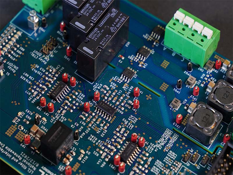
  • 2. Resins or Carriers

Resins form the base of rosin and no-clean flux. They provide viscosity and help residues stay stable.

  • 3. Solvents

Solvents keep the paste flexible during printing and help it spread properly. They evaporate at high temperatures.

  • 4. Additives

Additives control wetting, adhesion, viscosity, and residue color. They fine-tune performance for different use cases.

How to Use Soldering Paste? Types of Flux in Soldering

When everything works together, the flux streamlines the soldering process. It keeps the joint clean during heating, promotes good wetting, and improves overall reliability.

What Do You Do With Soldering Paste?

Solder paste has one main purpose: to bond components to PCB pads. But it offers other functions too. You can use solder paste for:

  • SMT soldering
  • Small electronic repairs
  • Replacing QFN, BGA, or fine-pitch ICs
  • Reflow soldering
  • Hot-air soldering
  • Tin filling on small pads
  • Creating small metallic joins on test boards

It is not only a bonding material. It also ensures proper alignment and contact. Component placement machines rely on the adhesive quality of paste to hold parts steady before heating. This prevents movement and reduces defects.

Solder paste is essential in almost every production environment. It helps create strong, reliable joints used in phones, computers, robots, medical devices, and industrial systems.

How to Use Solder Paste Correctly?

Using solder paste correctly is essential if you want stable joints and good yields. The process is simple, but every step matters. Here is a clear, step-by-step guide.
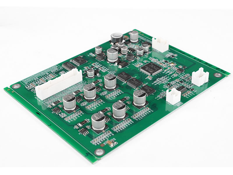
Step 1. Prepare the Surface

Clean surfaces lead to strong solder joints. Wipe pads with isopropyl alcohol if needed. Remove grease, dust, oxidation, and fingerprints.

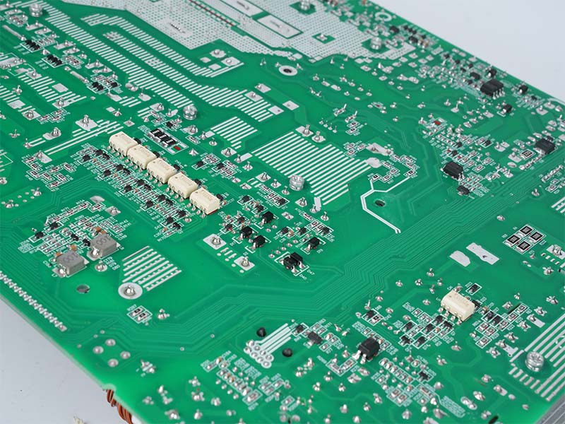
A clean pad helps the solder wet properly. Good wetting increases strength and lowers defect rates.

Step 2. Apply the Paste

There are two main ways to apply solder paste:

  • Method A: Stencil Printing

Most SMT factories use stainless steel stencils. The stencil spreads paste on each pad with controlled thickness. The print is clean, uniform, and repeatable.

  • Method B: Manual Application

For home repairs or prototypes, you can use a syringe. Push small dots of paste onto each pad. Keep the amount small and even. Too much paste can cause bridging.

Step 3. Place the Component

Place the component onto the pasted pads. The paste will hold it in place before heating. This tackiness prevents shifting. Manual tweezers or pick-and-place machines both work well.

Step 4. Heat the Joint

Reflow the paste using:

  • A reflow oven
  • A hot-air gun
  • A hot plate
  • An SMT rework station

The heat melts the alloy. Flux activates. Oxides break down. Wetting occurs. The solder shrinks into a glossy, stable joint.

Make sure you follow the correct temperature curve. Good reflow depends on controlled heating.

Step 5. Let It Cool

Cooling should be even and smooth. After cooling, inspect the joint. A good solder joint looks shiny and well-formed.

How to Use Soldering Paste? Types of Flux in Soldering

Do I Need Flux for Solder Paste?

You do not need extra flux when using solder paste. That is because solder paste already includes flux in its formula. The flux inside the paste is optimized for wetting, cleaning, and bonding.

Adding more flux may help in rare special cases, but it is usually unnecessary. Too much external flux may leave extra residue or cause splattering during heating.

What Happens If You Don’t Use Flux When Soldering?

Flux is essential when soldering bare wire or loose solder. Without flux, oxidation will remain on the metal surface. The solder will not wet properly. The joint becomes weak and unreliable.

Here are the common outcomes when flux is missing:

  • Poor wetting
  • Weak joint strength
  • Grainy or dull surface
  • Increased bridging probability
  • Higher defect ratio in production
  • Risk of intermittent electrical contact

These issues make flux a must-use material for any reliable soldering process.

Can Solder Paste Be Used on All Metals?

Solder paste works well with common PCB metals, such as:

  • Copper
  • Tin
  • Silver plating
  • Gold plating
  • ENIG finishes
  • HASL finishes
  • Immersion tin
  • Immersion silver

However, it does not bond effectively with some metals, such as:

  • Aluminum
  • Stainless steel (without special flux)
  • Nickel alloys (unless pre-treated)
  • Oxidized surfaces

If your metal surface resists wetting, you may need a specialized flux or pre-treatment.

How Long Does Soldering Paste Last?

Solder paste does not last forever. Over time, solvents evaporate, flux loses activity, and metal particles oxidize. All these factors weaken printing quality and reduce wetting.

Most solder pastes last:

  • Around 6 months refrigerated
  • Around 1 month at room temperature
  • Around 24 hours after opening, depending on humidity and airflow

To prolong lifespan, store it in a refrigerator around 2°C to 10°C. Warm it to room temperature before use. Do not open cold paste, or moisture will condense inside.

How to Use Soldering Paste? Types of Flux in Soldering

Common Problems When Using Solder Paste

Here are some issues that users may face, and what causes them.

  • 1. Bridging

Too much paste or misaligned stencils create solder bridges.

  • 2. Voids

Improper reflow or contaminated pads produce internal voids.

  • 3. Tombstoning

Uneven heating or different pad sizes cause components to lift.

  • 4. Incomplete Reflow

Low temperature prevents full melting.

  • 5. Slumping

Low-quality paste spreads too much before heating.

All these issues are easy to prevent with good control and proper technique.

Conclusion:

Solder paste is a powerful material that makes modern electronics possible. It supports clean joints, stable conductivity, and quick assembly.

If you need help with SMT production, solder paste selection, or high-precision PCB assembly, EBest Circuit (Best Technology) can support you with professional guidance and reliable manufacturing.

For inquiries, please contact: sales@bestpcbs.com

You may also like

Reliable Low Volume PCB Assembly Services for Fast Prototype

December 26th, 2025

Low Volume PCB Assembly​ bridges the critical gap between prototyping and full-scale production, providing a cost-effective method for functional testing and market validation. This article explores its key benefits, differentiates it from high-volume processes, and provides a guide for selecting the right partner to accelerate your product development.

Bringing a new electronic product to life is exhilarating, but the path from prototype to market is fraught with hurdles. What are the critical challenges teams face when sourcing assembled prototypes and small batches?

  • High upfront costs and MOQ barriers with standard assembly lines, making iteration financially risky.
  • Slow turnaround times due to complex setup and scheduling conflicts on high-mix, low-volume lines.
  • Compromised quality and reliability when using hobbyist services or incompatible assembly partners.
  • Lack of expert support and design feedback (DFM) to catch errors before manufacturing, leading to costly re-spins.
  • Inflexible processes that struggle with component sourcing for small quantities and frequent design changes.

The solution lies in partnering with a specialized Low Volume PCB Assembly Manufacturer​ whose processes are engineered for agility, quality, and support at smaller scales. Here is how the right partner addresses these core challenges:

  • Implements flexible pricing models with minimal to no MOQs, drastically reducing the financial risk of prototyping.
  • Optimizes workflows for speed, dedicating agile production cells to ensure fast prototype turnaround without sacrificing process rigor.
  • Applies the same stringent quality control (e.g., AOI, SPI, functional testing) as high-volume lines to guarantee reliability in every batch.
  • Provides proactive engineering support, offering comprehensive Design for Manufacturability (DFM) analysis to optimize designs before fabrication.
  • Maintains robust component sourcing networks and inventory management to handle shortages and last-minute changes efficiently.

As a professional Low Volume PCB Assembly Factory, BEST Technology combines state-of-the-art SMT lines with deep engineering expertise to deliver reliable Low Volume PCB Assembly services​ that are fast, scalable, and built to the highest quality standards. Whether you need FR4, flex, ceramic, or metal-based low volume PCB assembly services, we can support your build from prototype to small-batch production. We have 19 years of experience assembling all these board types.

Our core strengths include small-volume capability, multi-variety handling, fast delivery, and responsive service. Most of our customers come from Germany, the United States, and Israel, serving industries such as medical devices, industrial control, robotics, and IoT. For more information or if you would like to send us any inquiry, please send us an email through the contact form at the bottom of our Contact Page.

Low Volume PCB Assembly

What Is Low Volume PCB Assembly?

Low Volume PCB Assembly​ refers to the process of assembling printed circuit boards in smaller quantities, typically ranging from a single prototype to a few hundred units. This service is tailored for the research, development, and testing phases of product life cycles.

  • Core Purpose:​ It enables functional testing, design validation, and market pilot runs without the financial burden of large-scale production commitments.
  • Typical Applications:​ Prototyping for startups, pilot runs for OEMs, specialized industrial equipment, niche products, and R&D projects.
  • Key Differentiator:​ Unlike bulk production, it prioritizes flexibility, speed, and adaptability over the lowest possible per-unit cost.

The process follows the same core steps as standard PCB Assembly—solder paste application, component placement, reflow soldering, and inspection—but is optimized for efficiency at low quantities. The table below summarizes its key characteristics:

FeatureDescription
Order Quantity​1 to 500 units (varies by manufacturer)
Primary Goal​Speed, Flexibility, & Design Validation
Setup Emphasis​Quick turnaround and easy design changes
Cost Structure​Higher per-unit cost, lower total project cost

In summary, Low Volume PCB Assembly​ is the essential bridge between a validated design and mass production, allowing for iterative refinement with manageable risk.

Low Volume PCB Assembly

How Does Low Volume PCB Manufacturing Differ from High Volume Processes?

The fundamental difference lies in the core objectives: Low Volume PCB Manufacturing​ prioritizes flexibility and speed for development, while High Volume PCB Manufacturing​ maximizes efficiency and consistency for the market.

  • Flexibility vs. Optimization:​ Low-volume lines are built to handle a wide variety of designs with frequent changeovers. High-volume lines are fine-tuned for one design to maximize output.
  • Speed to First Article:​ The focus for prototypes is on getting the first working unit fast. For high volume, the focus is on achieving a stable, rapid production cycle.
  • Cost Perspective:​ Low volume considers total project cost and time-to-market savings. High volume strives to minimize the cost per individual unit.

Consider the following comparison across key parameters:

ParameterLow Volume PCB AssemblyHigh Volume PCB Manufacturing
Batch Size​1 – 500 units10,000+ units
Setup Time​Shorter, more frequentLong, optimized once
Line Flexibility​Very High (mixed technology)Low (dedicated to a product)
Primary Cost Driver​Engineering & Setup TimeMaterial & Scale Efficiency
Change Management​Easy and expectedDifficult and costly
Tooling​Often generic or soft-tooledCustom, hardened fixtures

Ultimately, choosing the right process depends on the product stage. For Fast Prototype​ and pilot needs, the agility of a Low-Volume PCB Assembly Factory​ is irreplaceable.

Why Do OEMs Rely on Wholesale Low Volume PCB Assembly for Pilot Production?

OEMs leverage Wholesale Low Volume PCB Assembly​ for pilot production because it de-risks scale-up by testing the manufacturability, supply chain, and performance of a product in a near-market environment.

  • Supply Chain Validation:​ A pilot run tests the real-world availability and compatibility of all components before committing to large-scale purchases.
  • Process Verification:​ It confirms that the assembly process designed in prototyping works reliably at a slightly larger scale, identifying potential yield issues.
  • Market Testing:​ Generates units for beta testing, regulatory certifications, and early customer feedback without massive inventory investment.
  • Logistics & Packaging Dry Run:​ Allows testing of the complete fulfillment cycle, from assembly to final packaging and shipping.

In essence, a pilot production run via a Wholesale Low Volume PCB Assembly Supplier​ acts as the final, critical check before the significant capital expenditure of mass production, ensuring a smoother and more predictable launch.

How Do Low Volume PCB Assembly Manufacturers Support Prototype Runs?

Specialized manufacturers support prototype runs by offering tailored services that go beyond simple assembly. They act as development partners.

  • Comprehensive DFM/DFA Analysis:​ Before assembly begins, engineers review design files to flag potential manufacturing, soldering, or reliability issues, suggesting modifications to improve yield and performance.
  • Rapid Turnaround:​ Dedicated quick-turn lines prioritize prototype orders, often offering services from 24-hour assembly to 5-day production turns.
  • Component Sourcing Support:​ They assist in procuring small quantities of components, managing the challenges of Minimum Order Quantities (MOQs) from distributors.
  • Mixed Technology Assembly:​ Capability to handle both SMT (Surface Mount Technology) and THT (Through-Hole Technology) on the same board, which is common in complex prototypes.
  • Rigorous Testing for Small Batches:​ Even for a handful of boards, they apply appropriate testing (e.g., flying probe, functional testing) to ensure each unit works as intended.

This holistic support system is what makes a Low Volume PCB Assembly Manufacturer​ a valuable asset for any development team, transforming a simple fabrication order into a collaborative engineering effort.

What Factors Shape Low Volume PCB Assembly Quotes During Early Development?

Understanding the components of a Low Volume PCB Assembly Quote​ empowers teams to make informed budgeting decisions. The cost is shaped by several key factors:

  • PCB Complexity:​ Layer count, size, material (e.g., standard FR-4 vs. ceramic), and special finishes (ENIG, immersion gold) directly impact the bare board cost.
  • Component Factors:​ The number of unique parts, their package sizes (fine-pitch components cost more to place), and source/availability. Obsolete or hard-to-find parts increase cost and time.
  • Assembly Difficulty:​ Mix of SMT vs. THT components, need for double-sided SMT placement, or any manual assembly steps.
  • Testing Requirements:​ The type and extent of testing (Visual Inspection, AOI, SPI, Functional Test) add time and labor but are critical for reliability.
  • Order Quantity & Turnaround:​ While per-unit cost decreases slightly with quantity, the total NRE (Non-Recurring Engineering) and setup costs are a larger portion of the total for very low volumes. Expedited turnaround incurs a premium.

A clear and detailed quote from a Low Volume PCB Assembly Supplier​ will break down these elements, providing transparency and helping you optimize the design for cost without compromising functionality.

Why Do Many Teams Choose China Low Volume PCB Assembly for Small-Batch Builds?

The choice of a China Low Volume PCB Assembly​ partner is often driven by a powerful combination of scale, skill, and value that is uniquely developed in the region’s electronics manufacturing ecosystem.

  • Integrated Supply Chain:​ Proximity to the world’s largest component manufacturers and PCB fabricators simplifies logistics, reduces lead times, and often provides cost advantages on the BOM (Bill of Materials).
  • Technical Expertise & Experience:​ Many Chinese factories have decades of experience servicing global clients, building deep expertise in handling diverse and complex projects for Low Volume PCB Assembly.
  • Advanced Manufacturing Infrastructure:​ Willingness to invest in the latest SMT equipment, automation, and testing gear to serve a sophisticated international market.
  • Cost-Effectiveness:​ Competitive labor and operational costs can translate to significant savings, especially valuable for startups and companies developing Cheap Low Volume PCB Assembly​ without sacrificing quality.

When selecting a China Low Volume PCB Assembly Manufacturer, the key is to vet partners for quality systems, communication skills, and experience with international standards to fully leverage these advantages.

What Should Buyers Evaluate When Selecting a Low Volume PCB Assembly Supplier?

Choosing the right partner is critical. Beyond just price, buyers should conduct thorough due diligence on several fronts to ensure a successful partnership.

Evaluation CriteriaKey Questions to Ask
Technical Capability​Can they handle your board’s technology (e.g., Boost Converter PCB Layout​ with high-current traces)? Do they offer DFM analysis?
Quality Certifications​Are they ISO 9001, IATF 16949, or ISO 13485 certified? What in-process quality controls (SPI, AOI) do they use?
Communication & Support​Is there a dedicated project manager? Are they responsive and proficient in your language? Do they provide clear Low Volume PCB Assembly Quotes?
Supply Chain Management​How do they handle component sourcing and shortages? Can they provide PCB Assembly Small Volume​ component kits?
Scalability​Can they support your product from 10 units to 10,000 units? Do they offer both Low Volume​ and High Volume PCB Manufacturing?

A supplier that scores well in these areas is more likely to be a reliable, long-term partner for your PCB Assembly Low Volume​ needs.

Why EBest Circuit (Best Technology) Is a Trusted Partner for Low Volume PCB Assembly?

As a reliable China low volume PCB assembly factory, BEST Technology​ has built its reputation by focusing exclusively on the challenges and requirements of low to mid-volume production. We understand that your prototype is not just a test board—it’s the foundation of your product’s future.

  • Dedicated Low-Volume Focus:​ Our processes, equipment, and team mindset are all optimized for agility, making us ideal for Fast Prototype​ and pilot production.
  • Engineering Partnership:​ We provide more than assembly; we offer expert design feedback to enhance manufacturability, reliability, and performance from the start.
  • End-to-End Control:​ From PCB Board Prototype​ fabrication to assembly and testing, we maintain strict quality control at every step, ensuring consistency and reliability.
  • Global Standard Quality:​ We serve demanding international clients, adhering to the highest global quality and communication standards, making us a reliable Low Volume PCB Assembly USA-alternative​ with competitive value.
Low Volume PCB Assembly

All in all, Low Volume PCB Assembly​ is the critical, strategic service that enables innovation by reducing the time, cost, and risk of bringing new electronic products to life. From validating a PCB Prototype​ to executing a pilot run, it provides the essential bridge between digital layouts and manufacturable boards.

This guide has outlined its importance, differentiated it from high-volume processes, and provided a framework for selecting the right manufacturing partner. For teams seeking reliable Low Volume PCB Assembly services for Fast Prototype​ development, BEST Technology​ stands as a proven partner. Pls feel free to contact our team at sales@bestpcbs.com to request a quote for your next project.

You may also like

0402 Resistor: Size, Values, Power Rating & Technical Details

December 24th, 2025

Surface-mount resistors are the backbone of modern miniaturized electronics, and the 0402 resistor package is one of the most widely used formats today. Designers rely on this small, lightweight device to save space, reduce cost, and support high-density PCB layouts. Although it looks very simple at first glance, the 0402 package plays a critical role in controlling current flow, establishing reference points, supporting bias networks, and maintaining signal integrity in compact circuits.

This guide provides a detailed and practical overview of the 0402 chip format, including 0402 resistor size, common resistance values, power rating, voltage performance, dimensional specifications, comparisons with smaller SMD formats, and the answers to common questions asked by designers.

0402 Resistor: Size, Values, Power Rating & Technical Details

What Is a 0402 Resistor?

A 0402 resistor is a surface-mount chip resistor with a physical size of 0.04 × 0.02 inches. It is designed to provide stable and predictable resistance in compact circuits. This package is widely used in mobile electronics, wearables, laptops, communication modules, IoT devices, industrial instruments, and automotive control units.

This small package is valued for its:

  • Very compact footprint
  • Low material and assembly cost
  • Stable electrical characteristics
  • High assembly efficiency in SMT production
  • Suitability for medium-density and high-density PCB layouts

The 0402 package sits at the center of the SMD resistor family. It is small enough for space-constrained layouts yet still large enough to offer good mechanical stability and predictable solder joint strength.

0402 Resistor Specifications and Dimensions

The specifications of a 0402 resistor vary by manufacturer, but the general characteristics remain fairly consistent across the market. Here is a 0402 resistor specifications and dimensions table:

ParameterTypical SpecificationNotes
Package Size (Imperial)0402Standard SMD code
Package Size (Metric)1005 (1.0 × 0.5 mm)ISO metric code
Length (L)1.00 mm ± 0.05 mmVaries by manufacturer
Width (W)0.50 mm ± 0.05 mmVaries slightly by series
Thickness (T)0.30–0.40 mmDepends on power rating
Terminal Thickness0.10 mmCu/Ni/Sn plated
Resistance Range0.5 Ω to 10 MΩWider ranges in some series
Tolerance Options±1%, ±2%, ±5%Thin-film supports ±0.5% or ±0.1%
Temperature Coefficient (TCR)±100 to ±400 ppm/°CPrecision film can reach ±25 ppm/°C
Power Rating0.0625 W (1/16 W)Enhanced versions reach 0.1 W
Maximum Working Voltage25 VLimited by small geometry
Dielectric Withstanding Voltage50 VShort-term withstand
Operating Temperature–55°C to +155°CTypical thick-film spec
Termination MaterialCu/Ni/SnLead-free RoHS compliant
Construction TypeThick-film or Thin-filmDepends on accuracy requirements
Standard PackagingTape & reel10,000 pcs or 5,000 pcs reels

Manufacturers offer both thick-film and thin-film construction. Thick-film versions are ideal for general-purpose applications due to their attractive cost. Thin-film versions provide tighter tolerance and lower TCR, which are preferred in precision circuits such as sensor interfaces and measurement systems.

What Size Is 0402 in mm?

The name “0402” reflects the imperial dimensions of the component. The first two digits represent the length in hundredths of an inch, and the last two digits represent the width in hundredths of an inch.

  • Length: 0.04 inch
  • Width: 0.02 inch

Converted to metric values, the 0402 package has:

  • Length: 1.0 mm
  • Width: 0.5 mm
What Size Is 0402 in mm?

Because of this small footprint, the 0402 format is widely used in circuits requiring tight component spacing. Designers select it when they need shorter trace lengths, denser routing, reduced board area, and improved electrical performance in compact RF or high-speed designs. The size also makes it suitable for smartphones, smart wearables, compact medical devices, and other highly integrated products.

What Are Typical 0402 Resistor Values?

Typical 0402 resistor values follow standard E-series ranges. This means the device is available in both common and precision resistance values across a wide span.

Common value ranges in 0402 packages include:

  • 1 Ω to 10 Ω for current sensing and damping
  • 10 Ω to 1 kΩ for signal biasing and termination
  • 1 kΩ to 100 kΩ for voltage dividers and control circuits
  • 100 kΩ to several MΩ for leakage control and pull-up or pull-down networks

In practical designs, engineers choose the value based on the required current, target voltage drop, allowed power dissipation, and noise or stability constraints. Many vendors provide full E24 and E96 series values for applications that require fine adjustment or precision tuning.

What Is the Voltage of a 0402 Resistor?

A typical 0402 chip has a modest voltage rating due to its very small physical size. A common set of values is:

  • Maximum working voltage: about 25 V
  • Dielectric withstand voltage: about 50 V

These numbers vary slightly between manufacturers, but the working voltage remains limited because the body is small and the internal conduction path is short. In sensitive or high-reliability designs, engineers normally operate these parts well below the maximum ratings.

When designing with these small chip resistors, you should consider:

  • Derating at high ambient temperature
  • Transient loads in switching circuits and startup events
  • Creepage and clearance distance on the PCB surface
  • Voltage coefficients, especially for very high resistance values

Even though the rated working voltage is around 25 V, many designers prefer to keep the operating voltage lower to minimize stress and improve long-term reliability.

What Is the Power Handling of 0402 Resistor?

The most common 0402 resistor power rating is:

  • 1/16 watt (0.0625 W)

Some specialized versions may offer ratings up to 0.1 W, but these parts rely on improved materials and specific manufacturing processes. Always review the datasheet before assuming a higher rating.

In real circuits, the actual power a 0402 can handle depends on more than the nominal rating. Key factors include:

  • Copper pad design and thermal connection to inner layers
  • PCB material and thickness
  • Ambient temperature and available airflow
  • Distance from other heat sources and power devices
  • Duration of load and duty cycle

Because the resistor is very small, its thermal mass is limited. It heats up quickly during overload. In high-density layouts, engineers often derate the load to around half of the nominal rating to ensure long service life and to avoid hot spots on the PCB.

What Is the Difference Between SMD 0201 and 0402?

The SMD 0201 and 0402 packages are both used in miniaturized designs, but they differ significantly in handling, manufacturability, and electrical behavior.

SMD 0201 Resistor

  • Size around 0.6 mm × 0.3 mm
  • Extremely small, with very limited pad area
  • Requires advanced pick-and-place machines and precise solder paste control
  • Usually has a lower power rating than 0402
  • More sensitive to misalignment, tombstoning, and reflow issues
  • Used mainly when PCB space is extremely constrained

SMD 0402 Resistor

  • Size around 1.0 mm × 0.5 mm
  • Easier to mount and inspect than 0201
  • Stronger solder joints and better mechanical stability
  • Higher power rating compared with 0201
  • Less prone to assembly defects in standard SMT lines
  • Broadly supported across many EMS factories and assembly partners

In simple terms, you can think of it this way: use 0201 when every square millimeter matters, and select the 0402 package when you want a good balance between size, stability, cost, and assembly yield.

0201 vs 0402 vs 0603 SMD Resistors

Specification020104020603
Metric Code060310051608
Dimensions (L × W)0.60 × 0.30 mm1.00 × 0.50 mm1.60 × 0.80 mm
Thickness0.23–0.33 mm0.30–0.40 mm0.45–0.55 mm
Typical Power Rating0.03 W0.0625 W0.1 W (some up to 0.125 W)
Max Working Voltage15–20 V25 V50 V
Resistance Range10 Ω to 1 MΩ0.5 Ω to 10 MΩ0.1 Ω to 22 MΩ
Tolerance Availability±5%, ±2%, ±1%±5%, ±2%, ±1%, ±0.5%±5%, ±2%, ±1%, ±0.5%, ±0.1%
TCR (ppm/°C)±200 to ±400±100 to ±400±50 to ±200
Assembly DifficultyVery highModerateEasy
Pick-and-Place CompatibilitySpecial nozzles requiredStandardVery standard
Rework DifficultyExtremely difficultManageableEasy
Tombstoning RiskHighMediumLow
Mechanical StrengthLowestMediumStrongest
Common ApplicationsUltra-compact wearables, RF modules, space-limited sensorsSmartphones, IoT devices, consumer electronicsIndustrial devices, power modules, automotive boards
Best ForMaximum densityBalance of size & stabilityBest reliability & ease of assembly

What Happens If I Use a Higher Ohm Resistor?

Using a higher resistance value than the original design changes the behavior of the circuit in a predictable way. Since current is given by I = V / R, increasing the resistance leads to a lower current flow.

The main effects are:

  • Lower current: the circuit draws less current through that branch
  • Higher voltage drop across the resistor: more voltage is lost on the component
  • Lower voltage at the load: some circuits may not receive enough voltage to operate properly
  • Reduced power consumption: in some bias networks this can be an advantage

In low-power applications, slightly increasing the resistance can be safe, and sometimes even helpful. However, if the resistor sets a gain, reference level, or timing constant, that change may cause unstable behavior or performance drift. When replacing values, always review the circuit function and check that the new value still meets the design requirements.

How Much Does an 0402 Resistor Weigh?

The weight of a single 0402 resistor is extremely low. Typical specifications list a figure in the range of:

  • About 0.4 mg to 0.6 mg per piece

For most projects this value is not critical. However, in aerospace, drone, and medical wearable designs, the total component mass can have a noticeable effect on product weight and battery life. The 0402 format offers a very attractive compromise: it is light enough for these demanding applications while still maintaining reliable solder joints and stable operation.

What Size Resistor to Drop 12V to 5V?

Sometimes designers want to use a resistor to drop voltage from 12 V down to 5 V for a small load such as a sensor or an indicator. This is not a very stable way to supply power for active electronics, but it is useful to understand the calculation.

First, calculate the required voltage drop:

  • Voltage drop needed: 12 V − 5 V = 7 V

If you know the load current, you can use Ohm’s law:

R = V / I

For example, if the load draws 20 mA:

  • R = 7 V / 0.02 A = 350 Ω

The power dissipated in the resistor is:

P = V × I = 7 V × 0.02 A = 0.14 W

This exceeds the common 1/16 W rating for a single 0402 part. You would either need a larger package, several resistors in parallel or series, or a different solution. In most cases, a linear regulator or DC-DC converter is the preferred way to reduce 12 V to 5 V for real circuits.

How to Read a 4 Digit SMD Resistor?

Many 0402 resistors are supplied without any marking because the surface area is so small. When a four-digit marking is present, the rule is straightforward.

  • The first three digits are the significant figures.
  • The fourth digit is the multiplier (power of ten).
How to Read a 4 Digit SMD Resistor?

Some examples:

  • 4702 means 470 × 10ÂČ = 47 kΩ
  • 1001 means 100 × 10Âč = 1 kΩ
  • 4993 means 499 × 10Âł = 499 kΩ

For precision E96 series, some manufacturers use alphanumeric codes instead of plain digits. These are often difficult to print on a 0402 body, which is why many devices in this size simply have no visible code and are identified only by packaging labels.

FAQs About 0402 Resistors

Can a 0402 resistor handle high-frequency signals?

Yes. Thin-film 0402 resistors offer low parasitic inductance and capacitance, which makes them suitable for RF and high-speed digital circuits. Layout quality and controlled impedance traces are still very important for best performance.

Are 0402 resistors difficult to hand solder?

They are small, but still manageable with the right tools. A hot-air rework station, fine-tipped soldering iron, good tweezers, and magnification help a lot. Beginners often practice with 0603 or 0805 packages before moving down to 0402.

What tolerance is recommended for precision circuits?

For analog, sensor, and RF designs, tolerances of ±1% or better are recommended. For general digital pull-up or pull-down networks, ±5% parts are usually enough and provide a better cost position.

Do 0402 resistors burn out easily?

They are reliable when used within their power and voltage ratings. Overload conditions, high ambient temperature, and poor thermal paths can cause overheating. Proper derating and layout design keep the risk of failure low.

What PCB land pattern should be used for 0402?

Most designers follow IPC-7351 or manufacturer-specific land pattern recommendations. These patterns are optimized to provide stable solder joints, consistent paste volume, and good inspection visibility.

Is thick-film or thin-film better for 0402?

Thick-film versions are cost-effective and widely used in consumer electronics. Thin-film versions provide lower noise, tighter tolerance, and more stable temperature behavior, making them ideal for precision circuits and high-end products.

Final Thoughts

The 0402 resistor is one of the most versatile and widely adopted SMD components in modern electronics. Its compact size, broad resistance range, predictable electrical performance, and compatibility with standard SMT processes make it an excellent choice for consumer devices, industrial control equipment, automotive modules, medical electronics, and compact IoT hardware.

By understanding its size, typical values, voltage rating, power rating, and application limits, engineers can make informed choices during PCB design and sourcing. Whether your priority is saving space, improving signal integrity, or optimizing assembly yield, the 0402 format delivers strong performance within an exceptionally small footprint.

You may also like

PCBA vs PCB: What Are the Differences?

December 24th, 2025

PCBA vs PCB describes two different stages of electronic product creation. A PCB is the bare printed circuit board with copper traces but no components. It provides structure and routing but cannot function on its own. A PCBA, in contrast, is the fully assembled board with all chips, resistors, capacitors, and connectors soldered in place, ready to power a device.

PCBA vs PCB: What Are the Differences?

What Is PCB in Electronics?

PCB is the base of most electronic products. It is the thin board that carries copper circuits. These copper paths guide signals and power across different parts of the device. A PCB does not power anything by itself. It only offers the layout and the structure.

PCBs use materials like FR4, aluminum, and ceramic. FR4 is the most common because it offers strength, stability, and a friendly price. Aluminum and ceramic boards are chosen for high-heat or high-frequency applications.

PCB can have one layer, two layers, or many layers. Because of this, PCBs can support small gadgets or advanced machines. Skilled designers use PCB technology to build phones, routers, sensors, medical devices, and even control units inside cars.

Are Motherboards Just PCBs?

A motherboard looks like a PCB, but it is much more than a bare board. It is a full PCBA. This means it contains the components, connectors, chips, capacitors, and controllers that allow a computer to function.

A pure PCB cannot run a processor, store data, or supply power. It needs components soldered onto it. When those parts are added, the board becomes a system board or motherboard.

So, a motherboard is not just a PCB. Instead, it is a perfect example of a PCBA. A motherboard is a product. A PCB is only a step toward that product.

How Are PCB Boards Manufactured?

Manufacturing PCBs is a complex process that requires precise operations at multiple critical stages to ensure the circuit boards possess excellent functionality, durability, and efficiency.

  • 1. Design and Layout

BEST Technology’s engineers use design software to create circuit layouts. We plan the routing of each copper trace, select the number of layers, and determine the hole size, pad shape, and width.

  • 2. Material Preparation

A large copper-clad sheet is chosen. The sheet uses FR4 or another base material.

  • 3. Image Transfer

The copper pattern is printed onto the board surface. This creates the shapes that guide the electrical signals.

  • 4. Etching

Excess copper is removed. Only the desired circuit pattern remains.

  • 5. Drilling

Small holes are drilled to connect layers or mount components.

  • 6. Plating

Copper is added inside the holes. This creates strong electrical connections.

  • 7. Solder Mask

The green (or red, blue, black) protective coating is applied. It prevents short circuits.

  • 8. Silkscreen

Text, symbols, and markings are printed for easy assembly.

  • 9. Surface Finish

A coating like ENIG, HASL, or OSP protects copper pads.

  • 10. Final Testing

Electrical tests ensure every circuit works.

This is how a PCB becomes ready for assembly. Next, components will be added. And that leads us to PCBA.

PCBA vs PCB: What Are the Differences?

Types of PCBs

PCBs come in different types. Each type serves a different purpose, and each one influences final product performance.

  • 1. Single-Sided PCB

One copper layer. Simple. Used for basic devices. Very low cost.

  • 2. Double-Sided PCB

Copper on both sides. More routing. Used in many everyday products.

Three or more layers. Often 4 to 32 layers. High performance. Great for complex electronics like PCs, routers, and industrial equipment.

High-Density Interconnect boards. Very fine lines. Laser-drilled microvias. Popular in smartphones, wearables, and advanced communication systems.

  • 5. Flex PCB

Thin and bendable. Used in cameras, medical probes, and folding designs.

A mix of rigid and flexible materials. Supports 3D structure. Trusted for aerospace and medical devices.

Uses aluminum or copper base. Excellent heat control. Great for LED lighting and power electronics.

When choosing between them, engineers consider temperature, size, frequency, and mechanical stress. Each board type offers a unique value and opens new design possibilities.

What Is a PCBA Board?

PCBA board is a PCB that has been assembled with electronic components. PCBA stands for “Printed Circuit Board Assembly.” It is the stage where the PCB receives the chips, resistors, sensors, and connectors that allow it to operate.

Without assembly, circuits cannot move data or power. With assembly, the board becomes a working product.

A PCBA can be simple or advanced. It may have only a few resistors, or it may have hundreds of parts with tight spacing. In fast-moving industries like consumer electronics, automotive, and medical devices, PCBA quality decides final product reliability.

PCBA vs PCB: What Are the Differences?

What Does PCBA Mean?

PCBA means the factory has placed and soldered components onto the bare board. The process includes:

  • Placement
  • Soldering
  • Inspection
  • Functional testing

People often confuse the terms “PCB” and “PCBA.” However, PCBA is the complete version, containing everything necessary for the device to function. PCB, on the other hand, is just the basic foundation.

What Are the Different Methods for PCBA Assembly?

Different devices require different assembly methods. Here are the most common ones.

  • 1. SMT (Surface Mount Technology)

The most popular method today. Components are placed on pads without holes. Machines place parts at high speed. Solder paste holds each part. Then heat melts the solder to make a strong joint.

SMT is great for compact, modern designs.

  • 2. Through-Hole Technology

Components have long legs. They go through holes in the board. Solder secures them on the opposite side. Through-hole is strong and dependable. It is often used for power components or connectors.

Even today, many industries use both SMT and through-hole together.

  • 3. Mixed Technology

Most boards use SMT for small parts and through-hole for strong or heavy parts. This balance offers performance and reliability.

  • 4. BGA Assembly

Ball Grid Array (BGA) components offer high density. They use solder balls under the chip. This method is used for processors, GPUs, and advanced modules.

  • 5. Wave Soldering

Hot solder flows in a wave. Through-hole parts get soldered at once. It saves time on mass production.

  • 6. Reflow Soldering

This method is for SMT parts. The board goes through a heating oven. The solder melts and bonds each pad.

Assembly technology keeps improving, but these core methods remain highly trusted in the industry.

What Is the Difference Between PCBA and PCB?

Now let’s talk about the main topic: PCBA vs PCB. This comparison is simple when explained clearly.

1. Structure

  • PCB: Just the base board with copper.
  • PCBA: Complete board with components.

2. Function

  • PCB: No function by itself.
  • PCBA: Can operate, run software, transmit signals, and power a device.

3. Stage

  • PCB: Step one of the process.
  • PCBA: Step two, after assembly.

4. Cost

  • PCB: Lower cost.
  • PCBA: Higher cost due to components, assembly, and testing.

5. Lead Time

  • PCB: Faster to produce.
  • PCBA: Takes longer due to sourcing, programming, and testing.

6. Use

  • PCB: For design verification, prototyping, and structure.
  • PCBA: For final products and field use.

7. Industry Terminology

PCB vs PCBA difference matters because many new buyers search for the wrong term. If you need a working board, you want PCBA—not just PCB.

PCBA vs PCB: What Are the Differences?

Conclusion:

PCBs form the structure. PCBs guide signals. PCBA processes signals. PCBs are the first step. PCBA is the final, functional product.

When you choose a professional PCBA manufacturer, your product gains reliability, performance, and trust.

For high-quality PCB and PCBA manufacturing in China and Vietnam, contact: sales@bestpcbs.com

You may also like