PCB manufacturing PCB manufacturing
Home > Blog

Motherboard PCB

What Is a Motherboard? Components, Functions and PCB Structure
Tuesday, August 4th, 2026

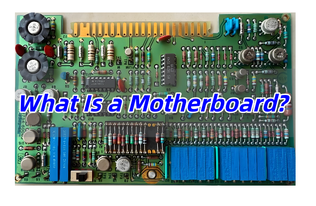
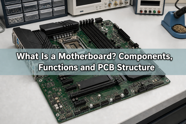
what is a motherboard? It is the main printed circuit board assembly in a computer. It distributes power, provides electrical paths between the processor, memory, storage and peripherals, and holds the sockets, connectors and control circuits that make those parts operate as one system. A motherboard does not perform every calculation itself; it provides the physical and electrical platform that lets each device exchange data reliably.
What Is a Motherboard? Components, Functions and PCB Structure

What Is a Motherboard and What Does It Do?

A motherboard, also called a mainboard, system board or mobo, is a populated PCB designed around a particular processor platform. It combines the bare circuit board with soldered devices, sockets, power converters, firmware memory, clocks and external interfaces. The CPU executes instructions, while the motherboard supplies the regulated power and communication routes the CPU needs to reach RAM, storage, graphics and I/O devices.

Its main functions are electrical rather than computational. The board converts incoming power into several lower-voltage rails, distributes clocks and reset signals, establishes high-speed links, stores startup firmware and exposes connectors that define how the computer can be expanded. A fault in any one of those paths can prevent booting even when the CPU and memory are undamaged.

What Components Are Found on a Motherboard?

Component placement follows signal length, power delivery, thermal and mechanical constraints. The CPU socket is kept close to memory and VRM circuitry; high-speed connectors are positioned to control routing length; and rear I/O is aligned with the chassis opening. The following groups explain what each visible area contributes.
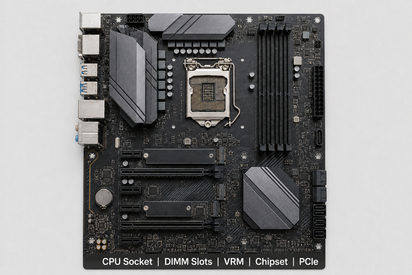
Core components on a modern computer motherboard
Component Primary role Important design dependency
CPU socket Mechanical and electrical interface for the processor Socket generation, pin map, keep-out area and cooler load
DIMM slots Connect system memory to the processor Memory generation, topology, trace matching and slot count
Chipset Manages platform I/O not connected directly to the CPU PCIe lanes, USB, SATA and firmware support
VRM Converts PSU input into stable low-voltage CPU and memory rails Current capacity, transient response, copper area and cooling
PCIe and M.2 connectors Connect graphics, storage and expansion devices Lane allocation, generation, bifurcation and signal integrity
BIOS/UEFI flash Stores platform initialization firmware CPU support, recovery method and update path
Rear I/O and headers Provide USB, network, audio, fan and front-panel connections Port count, controller bandwidth and chassis layout

How Does a Motherboard Work?

When the power button is pressed, standby power and control signals allow the PSU to start the main rails. The motherboard VRMs then generate the voltages required by the CPU, memory and chipset. After the rails and clocks stabilize, reset is released and the processor reads initialization code from the BIOS or UEFI flash device.

Firmware trains the memory interface, enumerates PCIe and storage devices, applies platform settings and selects a boot device. During normal operation, some high-bandwidth links run directly between the CPU and memory, graphics or primary storage. Other devices communicate through the chipset, which aggregates I/O before passing data to the processor. The board’s copper traces, reference planes, connectors and vias must preserve timing and signal quality across all of these paths.
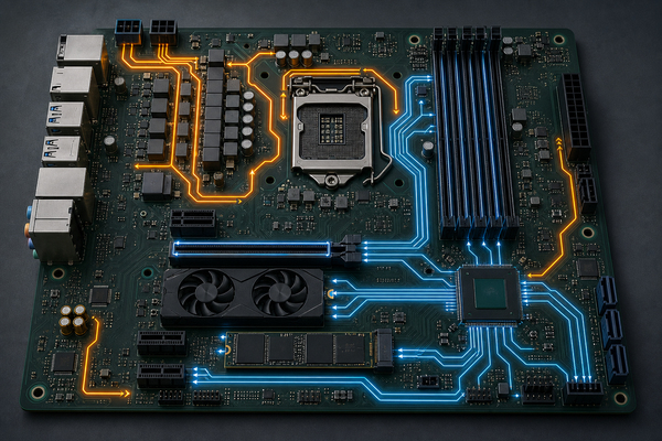
Power and high-speed data paths across a motherboard

What Is a Motherboard Chipset?

A motherboard chipset is the platform controller that expands the processor’s native interfaces. Modern CPUs often contain the memory controller and selected PCIe lanes, so the chipset no longer performs every function associated with older northbridge and southbridge designs. It commonly provides additional PCIe lanes, USB ports, SATA connections, networking interfaces and management functions.

Chipset choice affects available I/O and feature support, but the connector count printed on a product page does not reveal the complete topology. Several M.2 sockets, PCIe slots or high-speed USB ports may share uplink bandwidth or disable one another in particular configurations. A block diagram and lane-allocation table are therefore more informative than the number of physical connectors alone.

What Is a VRM on a Motherboard?

The voltage regulator module, or VRM, converts a 12 V input into the much lower voltage required by a processor or memory rail. A multiphase buck converter uses MOSFET power stages, inductors, capacitors and a controller to divide current among parallel phases. More phases can reduce current per phase, but controller quality, component ratings, switching behavior, copper area and thermal design matter more than a phase-count label by itself.

VRM layout is sensitive to loop inductance and heat concentration. Power stages and inductors are placed close to the CPU socket, while wide copper regions and internal planes carry high current. Thermal vias may spread heat into other layers or a backside area. Poor placement or insufficient copper can increase ripple, temperature and voltage droop during fast load changes.

What Are Motherboards Made Of?

Most computer motherboards use a multilayer flame-retardant epoxy-glass laminate with copper conductors, commonly described as FR4. The finished assembly also contains solder mask, surface finish, legend ink, plated holes, solder alloys, connectors and semiconductor packages. Material selection is tied to layer count, impedance control, thermal load, lead-free assembly temperature and long-term dimensional stability.

A typical stack-up alternates signal layers with power or ground reference planes. The planes lower return-path impedance and help contain electromagnetic fields, while controlled dielectric thickness and copper geometry establish the impedance of PCIe, USB, memory and other high-speed traces. Best Technology’s documented multilayer FR4 PCB capability extends to 32 layers, although the practical stack-up, drill structure and conductor limits still require engineering review for the specific design.
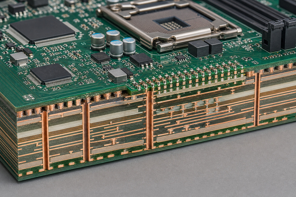
Illustrative multilayer motherboard PCB stack-up and copper interconnects

How Are Motherboards Manufactured?

Production begins with a verified stack-up and fabrication data set. Inner copper layers are imaged and etched, inspected, aligned with prepreg and copper foil, and laminated under heat and pressure. Mechanical or laser drilling creates through-holes and microvias. Desmear and copper plating make the hole walls conductive before outer-layer imaging, solder-mask application, surface finishing and electrical test.

Dense processor, chipset and memory fan-out may require blind vias or sequential lamination. An HDI PCB structure can reduce via-pad size and routing congestion, but it adds process steps and demands strict registration control. The correct build depends on BGA pitch, escape routing, layer count, aspect ratio and reliability targets rather than on board size alone.

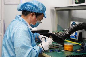
After bare-board fabrication, solder paste is printed, SMT components are placed and reflowed, and through-hole connectors are inserted and soldered. A motherboard combines fine-pitch ICs with large mechanical connectors, so paste volume, board support, thermal profiling and connector coplanarity need separate control. EBest Circuit (Best Technology) supports PCB assembly down to 01005 components and 0.25 mm BGA pitch, with 3D SPI, AOI and X-ray available for process verification.
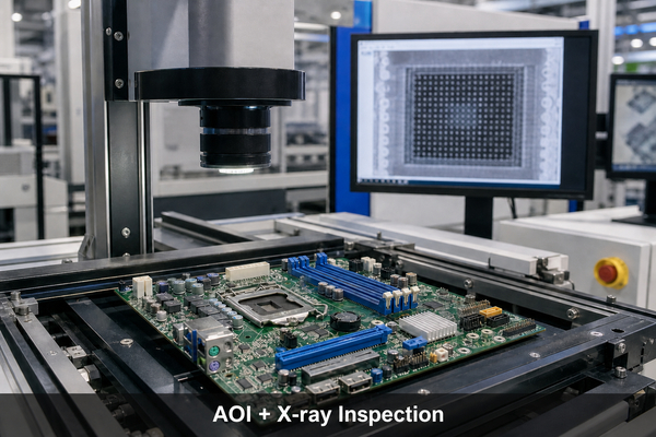
AOI and X-ray inspection of a motherboard PCBA

What Are the Main Motherboard Form Factors?

Form factor defines the board outline, mounting-hole locations and general expansion layout. It must match the enclosure and power-supply arrangement. Dimensions alone are not enough; cooler clearance, card spacing, connector access and cable routing also determine whether a board fits the system.

Form factor Common dimensions Typical design trade-off
ATX 305 × 244 mm More expansion slots and routing area, but requires a larger case
Micro-ATX 244 × 244 mm Smaller platform with fewer expansion positions
Mini-ITX 170 × 170 mm Compact system size with tight thermal and connector constraints
E-ATX Often about 305 × 330 mm; vendor definitions vary Additional area for memory, power and I/O, with chassis compatibility limits

Embedded and industrial motherboards may use other outlines or fully custom dimensions. Their connector placement is often driven by the enclosure, backplane, cooling path and service access rather than by a retail desktop standard.

How Do Motherboard Interfaces and Expansion Paths Work?

PCIe uses point-to-point serial lanes that can be grouped as x1, x4, x8 or x16 links. A graphics slot may receive lanes directly from the CPU, while additional slots, controllers and M.2 sockets connect through the chipset. M.2 describes the connector and module format; the installed device may use PCIe/NVMe, SATA or another supported interface.

High-speed routing requires controlled impedance, continuous reference planes, short via stubs and careful connector transitions. Differential-pair spacing and length matching are set for the applicable interface, but return-path continuity is equally important. A slot can be mechanically x16 while carrying fewer electrical lanes, and populating one connector can reduce bandwidth or disable another if the design shares resources.

How Does a Motherboard Differ From a PCB?

A PCB is the general platform of insulating material, copper conductors, holes and surface finish used to connect electronic components. A motherboard is a specific type of PCBA: a fabricated PCB populated with the processor interface, memory connectors, power conversion, firmware, I/O and expansion circuitry needed to coordinate a computer system.

The distinction is similar to the difference between a road network and a particular city built on that network. A bare motherboard PCB cannot function until components are assembled and programmed. For a deeper board-level comparison, see circuit board vs motherboard; the earlier guide to how a motherboard works in modern computers provides additional system context.

How to Choose a Motherboard?

Start with non-negotiable compatibility, then evaluate expansion and electrical margin. Marketing tiers are less useful than a platform diagram, supported-component list and connector map.

  • Match the CPU socket, chipset generation and BIOS version to the intended processor.
  • Confirm the board outline, mounting points, rear-I/O opening, cooler clearance and expansion-card space.
  • Verify the required memory generation, capacity, DIMM count and validated speed range.
  • Map GPU, M.2, PCIe, SATA and high-speed USB connections to their available lanes and sharing rules.
  • Check that the VRM and cooling design can sustain the processor’s real operating power, not only its nominal rating.
  • Confirm the required network, display, audio, fan, debug, security and firmware-recovery features.

For a custom motherboard, the same sequence begins at architecture level: processor and memory interfaces define the stack-up and routing density; enclosure and connectors define the outline; power and thermal analysis define copper distribution; and assembly/test access affects component placement.

FAQ

Can a PC Run Without a Motherboard?

No. A conventional PC needs a motherboard or an equivalent integrated system board to distribute power and connect the processor, memory, storage and I/O. Individual devices may power up separately, but they cannot operate as a coordinated computer without the interconnect and control platform.

Is the CPU the Motherboard?

No. The CPU is a semiconductor package that executes instructions. It installs into or is soldered onto the motherboard, which supplies power and connections to the rest of the system.

What Does a Motherboard Look Like?

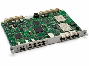
A desktop motherboard is usually a flat rectangular PCB with a prominent CPU socket, long DIMM and PCIe connectors, power connectors, several heatsinks and a rear-I/O cluster. Laptop and embedded boards often use irregular outlines and soldered processors to fit a specific enclosure.

Are Mainboard, System Board and Mobo the Same Thing?

They usually refer to the same primary circuit board. Mainboard and system board are common formal alternatives, while mobo is an informal abbreviation. In modular industrial equipment, however, a system may also contain backplanes, daughterboards or carrier boards with different roles.

Conclusion

Understanding what is a motherboard requires more than identifying sockets and ports. The board is a multilayer power and signal platform whose chipset topology, VRM, stack-up, vias, connectors, assembly process and inspection plan must work together. For custom motherboard PCB or PCBA support, EBest Circuit (Best Technology) can review the design against fabrication and assembly capabilities. Contact sales@bestpcbs.com with the project requirements.
You may also like

What Is a Motherboard? How a Motherboard Works in Modern Computers?
Friday, February 6th, 2026

What Is a Motherboard and Why Is It Called the Mainboard?

A motherboard is the central printed circuit board that connects every major component inside a computer. It acts as the electrical and mechanical foundation where the processor, memory, storage interfaces, and expansion devices communicate through controlled signal pathways. The term mainboard comes from early computer architecture, where one primary board coordinated multiple secondary cards. Over time, this main control board evolved into the highly integrated platform we now call a motherboard.

In modern systems, the motherboard is not just a passive connector. It integrates power regulation modules, high-speed data buses, firmware control, and thermal management features. Without it, individual components cannot exchange data or operate in a synchronized manner.

What Is a Motherboard? How a Motherboard Works in Modern Computers?

What Components Are Found on a Motherboard?

A typical motherboard combines several functional zones, each engineered for specific electrical and mechanical roles. Understanding these sections helps beginners visualize how the entire system operates.

Common motherboard components include:

  • CPU Socket – The interface that holds the processor and routes power and signals through dense pin arrays.
  • Chipset – A controller hub managing communication between CPU, memory, storage, and peripheral devices.
  • DIMM Slots – Memory connectors designed for controlled impedance and high-frequency signal integrity.
  • VRM (Voltage Regulator Module) – Converts input power into stable voltages required by the CPU and GPU.
  • PCIe Slots – High-speed expansion interfaces for graphics cards, AI accelerators, or networking modules.
  • Storage Connectors – SATA ports and M.2 slots enabling SSD and HDD integration.
  • BIOS/UEFI Chip – Firmware storage that initializes hardware during system startup.
  • Rear I/O Ports – External interfaces such as USB, Ethernet, audio, and video outputs.

Each element is strategically placed to balance thermal airflow, signal routing length, and electromagnetic compatibility.

How Does a Motherboard Work Inside a Computer System?

A motherboard operates as a complex communication network. Instead of moving data randomly, it directs information through predefined pathways called buses and layers within the PCB stack-up.

When a computer powers on, the firmware activates the CPU and checks connected devices. The chipset coordinates traffic between components. For example, when software loads from an SSD, the motherboard routes data from storage through PCIe lanes to the processor and then to memory modules.

Power distribution is equally important. The VRM converts raw power from the power supply into precise voltage rails. These rails must remain stable even under heavy computational loads. High-quality motherboard designs use multi-phase power circuits and thick copper layers to reduce heat and electrical noise.

Modern boards also support advanced features such as:

  • High-speed DDR memory signaling
  • Multi-layer impedance control
  • Thermal sensors and fan control logic
  • Firmware-based hardware monitoring

Together, these functions transform the motherboard into the coordination center of the entire computer.

Types of Motherboards

Motherboards vary widely depending on device size, performance targets, and application environments. Engineers often classify them by form factor and usage scenario.

Common motherboard categories:

TypeTypical UseCharacteristics
ATXDesktop PCsBalanced expansion slots and cooling space
Micro-ATXCompact desktopsReduced size with moderate expandability
Mini-ITXSmall systemsMinimal footprint, limited slots
Server MotherboardData centersMulti-CPU support, ECC memory
Industrial MotherboardAutomation systemsLong lifecycle, rugged design

Form factor determines mounting holes, connector placement, and airflow design. It also influences PCB layer count and routing complexity.

Why Is Motherboard PCB Design Important for Performance?

Motherboard performance is strongly linked to PCB engineering rather than just component selection. High-speed signals travel through copper traces at gigahertz frequencies. Poor routing can introduce signal reflection, crosstalk, or impedance mismatch.

Key PCB design considerations include:

  • Layer stack-up planning for controlled impedance
  • Power plane separation to minimize noise
  • Thermal via arrays for heat dissipation
  • Differential pair routing for PCIe and USB interfaces
  • Ground reference integrity to maintain signal stability

Advanced motherboard PCBs often use 6 to 14 layers or more. These layers allow engineers to separate power, ground, and data channels, ensuring reliable high-speed communication.

What Materials Are Used in Motherboard Manufacturing?

Most consumer motherboards are built using high-performance FR-4 laminate materials. However, not all FR-4 substrates are identical. Manufacturers select materials based on thermal stability, dielectric constant, and mechanical durability.

Typical materials used:

  • High Tg FR-4 – Provides better resistance to heat during soldering and long-term operation.
  • Low-loss dielectric materials – Used in high-frequency server or workstation boards.
  • Copper Foil (1oz–2oz) – Determines current-carrying capability and thermal spreading.
  • Solder Mask & Silkscreen – Protect circuitry and guide assembly processes.

Server-grade motherboards sometimes use low-Dk materials to maintain signal integrity across long PCIe lanes, especially for AI or data-center applications.

Desktop vs Server vs Industrial Motherboard — What’s the Difference?

Although all motherboards share similar architecture, their design priorities differ significantly depending on application environments.

FeatureDesktop MotherboardServer MotherboardIndustrial Motherboard
Performance FocusGaming or daily tasksHigh computation & uptimeReliability & longevity
Memory SupportStandard DDRECC Registered memoryOften fixed configurations
ExpansionGPU-centricMultiple PCIe lanesLegacy interfaces supported
Operating EnvironmentControlled indoorData center racksHarsh industrial conditions

Desktop boards prioritize user customization. Server boards emphasize redundancy and remote management. Industrial boards focus on durability, extended supply cycles, and stable operation in demanding environments.

How to Choose the Right Motherboard for Your Application?

Selecting a motherboard begins with defining system requirements rather than comparing brand names alone.

Consider these factors:

  • Processor compatibility and socket type
  • Memory capacity and speed
  • Number of PCIe lanes required
  • Thermal design and airflow
  • Long-term availability for industrial or embedded products
  • Power delivery capability for high-performance CPUs or GPUs

Engineers designing custom hardware often review PCB layer count and VRM layout because these parameters directly affect system stability during peak loads.

What Problems Do Beginners Often Face When Learning About Motherboards?

New learners frequently focus only on visible connectors while overlooking electrical design principles. Some common challenges include:

  • Confusing chipset roles with CPU functionality
  • Assuming all motherboards offer identical performance
  • Ignoring power delivery limitations
  • Underestimating signal integrity requirements
  • Misunderstanding compatibility between form factors

Learning basic PCB architecture helps beginners grasp why certain boards support higher memory speeds or more expansion devices.

What Is the Difference Between a Motherboard and a PCB?

A PCB refers to the physical board that holds copper traces and electronic components. A motherboard is a specialized type of PCB designed specifically to integrate computing subsystems.

Key differences:

  • A PCB can be simple or complex, used in any electronic device.
  • A motherboard is a multi-layer, high-density PCB with integrated computing infrastructure.
  • Motherboards require stricter impedance control, thermal management, and power distribution compared with general PCBs.

In short, every motherboard is a PCB, but not every PCB qualifies as a motherboard.

FAQs

1. Is the motherboard responsible for system speed?

Yes, indirectly. While the CPU and memory define raw performance, motherboard design determines how efficiently these components communicate.

2. Can a motherboard be upgraded easily?

It depends on the system. Desktop boards are usually replaceable, while laptops and industrial systems often use fixed designs.

3. How many PCB layers does a modern motherboard use?

Most consumer boards use 6–8 layers, while high-end server boards may exceed 12 layers to support complex routing.

4. Does motherboard size affect performance?

Size itself does not increase speed, but larger boards typically allow better power delivery and more expansion options.

5. Why do server motherboards cost more?

They include advanced reliability features such as ECC memory support, redundant power paths, and extended validation processes.

You may also like

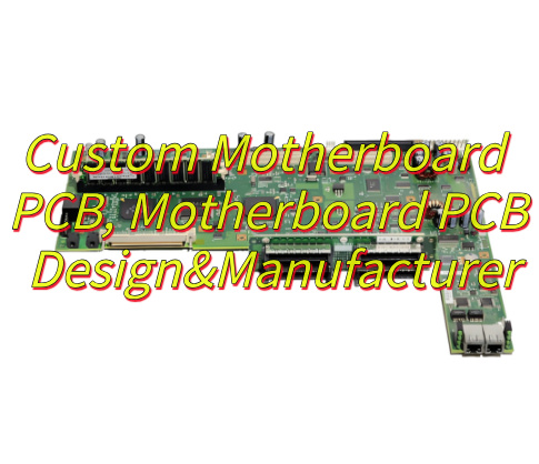
Custom Motherboard PCB, Motherboard PCB Design&Manufacturer
Wednesday, May 28th, 2025

Are you looking to create a custom motherboard PCB that balances performance, reliability, and cost-effectiveness for your next project? In this comprehensive guide, we’ll explore the key considerations for designing and manufacturing custom motherboard PCBs, from layer optimization to material selection and thermal management.

At EBest Circuit (Best Technology), we’ve been delivering custom motherboard PCB solutions for over 20 years, combining advanced engineering expertise with state-of-the-art manufacturing capabilities. Our services include end-to-end support—from motherboard PCB design and prototyping to high-volume production. We specialize in multi-layer boards (up to 32 layers) and high-frequency applications, offering free DFM analysis to eliminate design flaws and reduce costs. With 24-hour expedited prototyping, ISO-certified quality control, and transparent pricing, we ensure your project stays on schedule and within budget.  Feel free to contact us: sales@bestpcbs.com.

What Is Custom Motherboard PCB? 

A custom motherboard PCB is a printed circuit board designed to meet specific functional, physical, and performance requirements for computing systems. Unlike generic motherboards, custom PCBs integrate unique features such as specialized connectors, power management modules, or high-speed signal paths. During assembly, these PCBs undergo a precise process where components like integrated circuits, resistors, and capacitors are soldered onto the board using surface mount technology (SMT) or through-hole technology. This meticulous assembly ensures that each custom motherboard PCB functions optimally, delivering the tailored performance that its design demands.

Custom Motherboard PCB

How to Custom the Layer Design of Motherboard PCB?

Layer design is critical for motherboard PCB design, as it directly impacts signal integrity, power efficiency, and manufacturability. Here’s a step-by-step approach: 

  • Route with Clearance: Maintain a minimum clearance of 8-10 mils between traces to avoid short circuits. Ensure that high-voltage traces have even greater separation to prevent arcing.
  • Plan for Thermal Management: Incorporate thermal vias to efficiently transfer heat from power components to internal layers. Use thermal relief patterns around pads to prevent soldering issues caused by excessive heat.
  • Design for Testability: Include test points on critical signals for easy access during manufacturing testing. Ensure test points are placed away from components to allow for automated test equipment (ATE) probing.
  • Classify Signal Types: Separate high-speed signals (e.g., PCIe, USB) from low-speed signals (e.g., GPIO) to minimize crosstalk. Use dedicated ground planes between signal layers for isolation.
  • Determine Layer Count: Start with a 4-layer stack-up (2 signal layers, 1 power plane, 1 ground plane) for basic designs. For complex systems, add layers for differential pairs or embedded components.
  • Optimize Stack-up: Place analog and digital signals on separate layers to reduce EMI. Use symmetric layer structures to prevent warping during thermal cycling.
  • Control Impedance: Calculate trace widths and dielectric thicknesses to achieve target impedance (e.g., 50Ω for USB 3.0). EBest Circuit (Best Technology) offers ±10% impedance tolerance for values >50Ω and ±5Ω for ≤50Ω .
  • Manage Vias: Use buried or blind vias for HDI boards to reduce layer count. Ensure vias are spaced at least 12 mil apart to avoid copper cracking.
Custom Motherboard PCB

How to Select the Material of Custom Motherboard PCB?

Material choice influences thermal stability, electrical performance, and cost. Here’s a breakdown of common options: 

  • FR4: The industry standard for most motherboards, offering a balance of mechanical strength and thermal resistance (TG ~130–180°C). Ideal for consumer electronics. 
  • Rogers: High-frequency materials with low dielectric loss (Dk ~2.2–3.0), suitable for 5G, Wi-Fi, or RF applications. 
  • Metal-Core PCBs: Aluminum or copper substrates for enhanced heat dissipation, used in power-hungry components like GPUs. 
  • High-TG FR4: TG >180°C for automotive or industrial environments with extreme temperatures. 

Consider factors like operating temperature, signal frequency, and budget. EBest Circuit (Best Technology) stocks materials from Rogers, Dupont, and other leading suppliers, ensuring compatibility with your design requirements. 
How to Design Motherboard PCB Circuit Layout for Signal Integrity? 

Signal integrity is paramount in motherboard PCB design, especially for high-speed interfaces. Follow these guidelines: 

  • Minimize Crosstalk: Route high-speed signals (e.g., clock lines) perpendicular to adjacent layers. Maintain trace spacing of at least 3x the trace width.
  • Differential Pair Routing: Use matched-length pairs for USB, HDMI, or Ethernet to reduce EMI. Ensure impedance matching within ±10%.
  • Ground Plane Continuity: Avoid splits in ground planes, as they disrupt signal return paths and increase noise. Use stitching vias to connect fragmented ground planes.
  • Termination Techniques: Add series resistors or AC coupling capacitors to prevent signal reflections. For low-voltage differential signaling (LVDS), use parallel termination at the receiver.
  • Layer Stack-up Optimization: Select appropriate dielectric materials with low loss tangent values and carefully balance the number of signal and power/ground layers to control impedance and reduce signal attenuation.
  • Avoid Sharp Corners: Use rounded or 45-degree angles when routing traces instead of sharp 90-degree corners to minimize signal reflections and electromagnetic radiation.
  • Power Plane Decoupling: Place decoupling capacitors close to the power pins of integrated circuits. Use a combination of different capacitor values (e.g., 0.1 μF and 10 μF) to cover a wide range of frequencies and reduce power supply noise.
  • Signal Isolation: Separate sensitive analog signals from noisy digital signals by creating physical barriers or using dedicated layers and routing strategies to prevent interference.
Custom Motherboard PCB

How to Optimize PCB Motherboard Thermal Management Design? 

Effective thermal management prevents component degradation and extends product lifespan. Implement these strategies: 

  • Copper Thickness: Use 2–3 oz copper for power planes to handle high currents. EBest Circuit (Best Technology) supports up to 30 oz copper for extreme applications.
  • Heat Sink Integration: Design thermal vias under hot components (e.g., CPUs) to transfer heat to the chassis. Use thermal interface materials (TIMs) for better conductivity.
  • Fan Placement: Position fans near high-power components, ensuring airflow paths avoid stagnant zones. Use CFD simulations to validate cooling efficiency.
  • Thermal Relief Pads: Add relief pads around through-hole components to prevent solder joint fatigue from thermal expansion.
  • Layer Stack-up Optimization: Incorporate additional internal copper layers dedicated to heat spreading, increasing the overall thermal conductivity of the PCB and enabling more efficient heat dissipation across the board.
  • Component Layout Strategy: Group heat-generating components together in an area of the PCB with ample space for ventilation, separating them from heat-sensitive components to minimize thermal interference.
  • Surface Finish Selection: Choose a surface finish with good thermal properties, such as immersion silver or electroless nickel immersion gold (ENIG), which can enhance heat transfer from components to the PCB surface.
  • Vented Enclosure Design: If applicable, coordinate the PCB design with the enclosure, creating vents or openings that align with the natural airflow patterns on the board to allow hot air to escape and cool air to enter.
  • Heat Pipe Incorporation: Integrate heat pipes into the PCB design for critical components. Heat pipes can rapidly transfer heat from high-temperature areas to cooler regions, effectively spreading heat across a larger surface area for improved cooling.
Custom Motherboard PCB

How to Choose A Trusted Custom Motherboard PCB Manufacturer? 

Selecting the right manufacturer ensures your design is executed flawlessly. Look for:

  • Technical Expertise: Experience in multi-layer PCB design, HDI, and high-frequency applications. EBest Circuit (Best Technology)’s 20+ engineers provide SI/PI analysis and DFM checks.
  • Advanced Design Tools: Utilization of industry-standard software like Altium Designer, Or CAD, and PADS for precise and efficient PCB design.
  • Material Options: Offering a wide range of PCB materials including FR-4, Rogers, and high TG laminates to suit different performance requirements.
  • Certifications: ISO 9001, IATF 16949 for automotive/aerospace compliance.
  • Prototyping Capabilities: Rapid turnaround (24–72 hours) for proof-of-concept testing.
  • Flexible Prototyping: Support for both rigid (like FR4 PCB, MCPCB) and flexible PCB prototypes, enabling versatile product development.
  • Quality Control: AOI, X-ray, and functional testing to ensure zero defects. EBest Circuit (Best Technology)’s 70+ quality checks include automated optical inspection and impedance testing.
  • Traceability: Full traceability of materials and manufacturing processes for complete quality assurance.
  • Transparent Communication: Real-time WIP updates and dedicated project managers.
  • Customized Reporting: Providing detailed reports on design, manufacturing, and testing for clients’ records and analysis.

Can Your Manufacturer Support Custom Motherboard PCB Prototyping? 

Yes. EBest Circuit (Best Technology) offers custom motherboard PCB prototyping with 24-hour expedited service for urgent projects. Our process includes: 

  • Design Review: Free DFM analysis to identify manufacturability issues. 
  • Material Selection: Access to FR4, Rogers, and other specialty materials. 
  • Rapid Fabrication: 2-layer boards in 24 hours, 4-layer in 48 hours, and 6–8-layer in 72 hours. 
  • Testing: Comprehensive electrical and mechanical tests to validate performance. 

How Can We Deliver Custom Motherboard PCB Prototypes in 48-72 Hours? 

To achieve 72-hour delivery, we: 

  • Prioritize Urgent Orders: Dedicated production lines for prototypes. 
  • Streamline Communication: Direct access to engineers for quick design adjustments. 
  • Pre-Approved Materials: Stocked inventory of common materials to eliminate delays. 
  • Express Shipping: Partner with DHL/FedEx for global delivery within 24–48 hours. 

At EBest Circuit (Best Technology), we understand the importance of speed without compromising quality. Our prototyping services are backed by 18+ years of manufacturing experience and ISO-certified processes, ensuring your prototype meets or exceeds expectations.

You may also like