USB pinouts are an essential component of USB technology, enabling accurate data and power transfer between devices using the USB standard. Familiarizing yourself with USB pinout diagrams and troubleshooting USB pinout issues can help you diagnose and resolve USB connectivity, data transfer, and power delivery issues. Whether you’re developing and building USB devices or connecting and charging devices using USB technology, understanding USB pinouts is crucial to maximizing the potential of USB technology.
USB Type-C (2025 Standard)
8-Pin Simplified Version (Charging + Basic Data Transfer)
Symmetrical Pins: GND, VBUS, D+/D-, CC1/CC2
Supports reversible insertion, using CC1/CC2 to detect insertion orientation and negotiate power protocols.
Full 24-pin Version (Supports High-Speed Data Transfer)
Includes TX/RX differential pairs (USB 3.2/4 compatible), SBU sideband signals, and more, supporting 100W fast charging and 40Gbps data transfer.
Type-A/B (Legacy Interface)
Type-A (Commonly Used on Computers)
4-pin: GND, VBUS, D+, D-, supports USB 2.0 data transfer.
Type-B (Used for Printers and Other Devices)
5-pin: Adds a ground pin for compatibility with more devices.
Mini/Micro USB
Typically uses a 4-pin design: GND, VBUS, D+, and D-, suitable for low-power devices.
Key Pin Functions
VBUS: Main power pin (adjustable from 5V to 20V).
D+/D-: USB 2.0 data transmission.
CC1/CC2: Detect insertion direction and negotiate the fast charging protocol.
What is a USB Pinout?
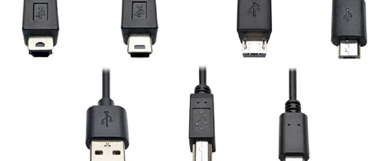
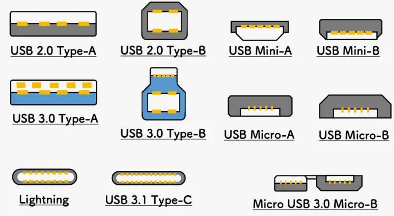
The USB pinout is the pin configuration of a connector and how it transfers data and power. Each USB connector has a unique pinout and function. Depending on the connector, USB has four or five pins. Type A, Type B, Mini-USB, and Micro-USB connectors are the most popular.
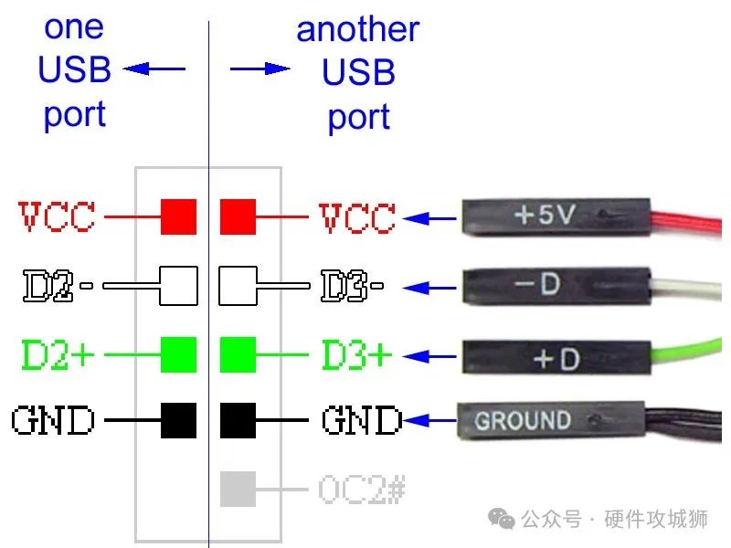
The most popular USB connector, Type A, contains four pins: two data pins (D+ and D-) and two power pins (VCC and GND). The power pins power the device, while the data pins transfer data.
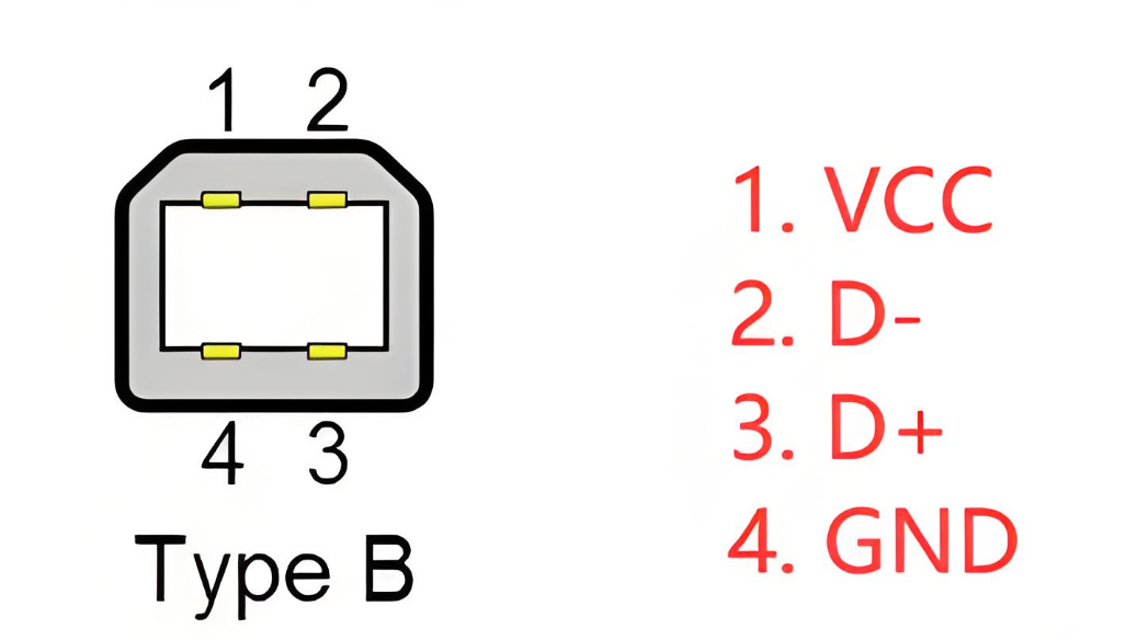
Printers, scanners, and other power-consuming devices use a Type B connector. It contains five pins: two data, two power, and one ground. Like Type A connectors, Type B connectors contain a ground pin as well as data and power pins.
Cameras, mobile devices, and tablets often use Mini-USB or Micro-USB connections for charging and data transfer. Two power pins, two data pins, and one ground pin form the standard configuration for these ports. Mini-USB and Micro-USB connectors have fewer data and power pins than Type A and Type B connectors.
USB connector data pins transmit digital signals. The D+ and D- pins encode and decode data during transmission. DC voltage is provided through the power pins to power connected devices.
The USB pinout defines the connector’s pin layout and how it transmits data and power. Understanding USB connector types and pinouts is essential for troubleshooting and connecting devices.
USB Data Transfer
USB data transfer is the process of exchanging information between two USB-enabled devices. Digitally stored information can take many forms, from still images to moving images. The USB protocol defines the rules for data transfer between devices connected via USB.
The multi-layered architecture of the USB protocol includes the physical layer, the data link layer, and the application layer.
These layers work together to ensure error-free information exchange between devices. USB cables and connectors are part of the physical layer, which also specifies the electrical characteristics of the signals. The application layer specifies the nature of the data exchanged, while the data link layer controls how data moves between devices.
Bulk, interrupt, isochronous, and control transfers are the various types of data transfers available on USB. Interrupt transfers are used for keyboard and mouse input, while bulk transfers are used for larger data transfers, such as file transfers. Real-time data transfers, such as audio and video streaming, use isochronous transfers, while device configuration and status updates use control transfers.
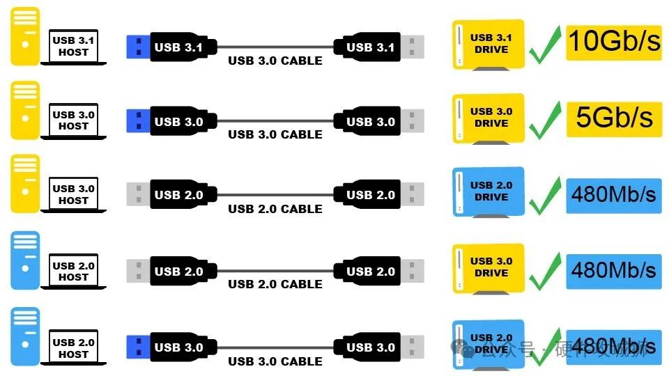
USB speeds vary by version. USB 2.0 has a data transfer speed of 480 Mbps, while USB 1.1 has a data transfer speed of 12 Mbps.
USB 3.2 allows for data transfer speeds of 20 Gbps. USB data transfer speed and reliability depend on the quality of the USB cable. Type-A, Type-B, Mini-USB, Micro-USB, and USB-C cables are available in various lengths and types.
USB Power Delivery
USB Power Delivery (USB-PD) allows devices to charge faster over USB cables. USB-PD uses the USB Type-C connector and cable and extends the USB standard. The USB-PD protocol allows the host and device to negotiate power, delivering up to 100W of power over the USB cable. This is a significant increase from the 2.5W of USB 1.0 and 2.0 and the 7.5W of USB 3.0.
USB-PD can charge multiple devices, laptops, and other high-power devices simultaneously and faster. USB-PD allows devices to negotiate power for optimal charging.
USB-PD supports the USB Type-C connector, which is a major advantage. The reversible USB Type-C connector is easier to use. With its higher data transfer speeds and 100W power delivery, it can charge laptops and other high-power devices.
USB Power Delivery can also power monitors and connect peripherals. USB-PD powers monitors without a power cable. USB-PD also powers and connects docking stations and external hard drives.
USB Power Delivery allows devices to charge faster using a USB cable. USB Power Delivery uses the USB Type-C connector and cable and extends the USB standard. USB-PD can simultaneously charge multiple devices, laptops, and other high-power devices at a faster rate. USB-PD can also power monitors and connect devices.
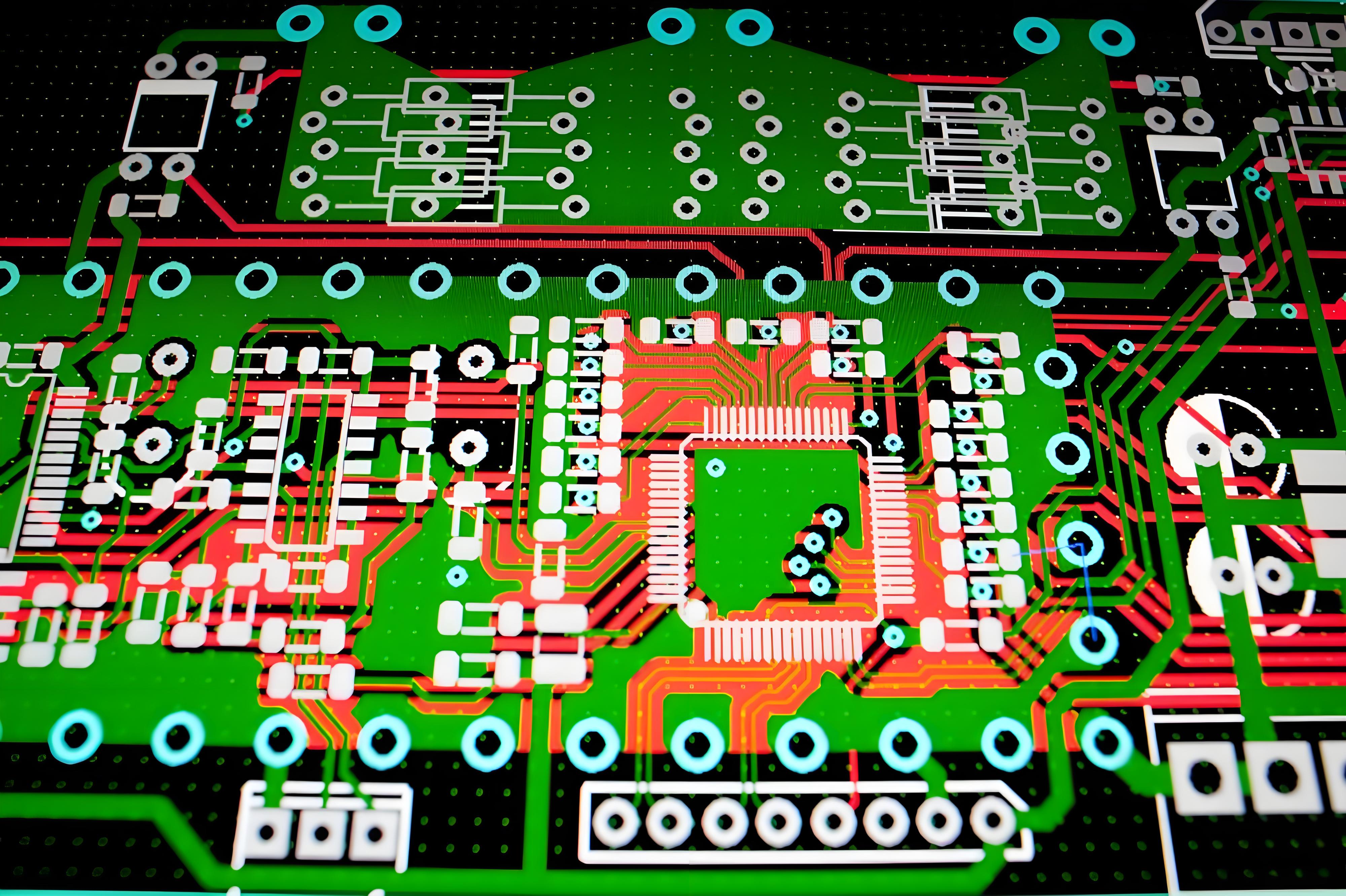
USB Pinout Diagrams
USB cable wiring and connections can be visualized with the help of pinout diagrams. Type-A, Type-B, Mini-USB, Micro-USB, and USB-C are just a few of the available USB connector types. Pinout diagrams showing the connector configuration and functionality are available for each type.
USB Pinout: USB Type-A
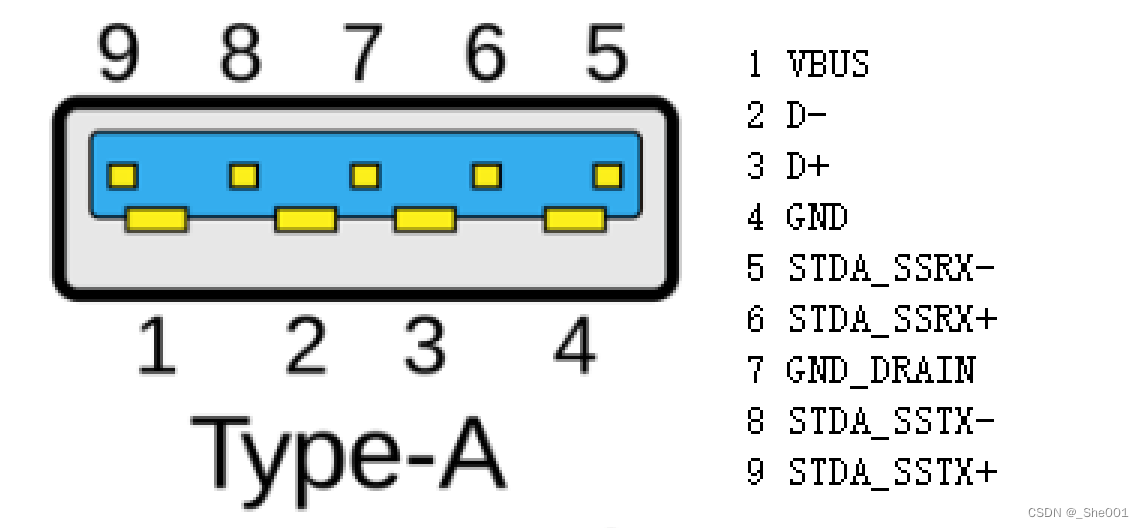
The most commonly used USB connector is the USB Type-A connector, which is used to connect peripheral devices to a computer. The USB Type-A pinout consists of four pins, labeled VBUS (power), D+ (data), D- (data), and GND (ground). Data is transferred between the device and the computer via the D+ and D- connections, while the VBUS pin provides power to the device. The GND pin provides electrical ground. If you are experiencing issues with USB connectivity, data transfer, or power, a USB Type-A pinout diagram may be helpful.
USB Pinout: USB Type-B
USB Type-B connectors are commonly used for devices such as printers and scanners that connect to a computer. The USB Type-B pinout diagram includes five pins: VBUS (power), D+ (data), D- (data), GND (ground), and ID (identification).
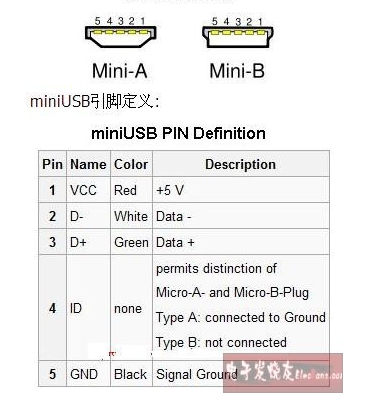
USB Pinout: Mini-USB
The Mini-USB connector is a more compact version of the USB Type-B connector. This connector is commonly found in mobile phones and other portable electronic devices. VBUS (power), D+ (data), D- (data), GND (ground), and ID are the five pins included in the Mini-USB (identification) pinout diagram.
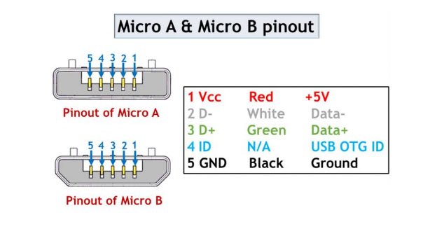
Micro-USB Pinouts
The USB connector is a smaller variant of the USB connector and is commonly used in small devices such as smartphones. Its pinout diagram has five pins: VBUS (power), D+ (data), D- (data), GND (ground), and ID (identification).
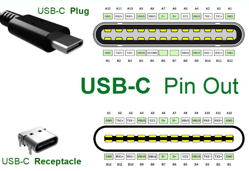
USB-C Pinouts
Newer devices have a USB-C connector. It provides faster data transfer and charging and can be inserted in either direction. USB-C has 24 power, data, and other pins.
In summary, USB pinout diagrams provide a visual representation of USB cable wiring and connectors. There are several types of USB connectors, each with its own pinout diagram. Understanding these diagrams may be helpful when debugging USB connection issues or developing and building USB devices.
USB Connection Troubleshooting
Connection, data transfer, and charging issues are just some of the problems that can arise from incorrect USB pinouts. To troubleshoot USB pinout issues, use the following troubleshooting steps:
Step 1 – Check the Cable Condition
Make sure the USB cable you’re using is undamaged and in good working order. Aggravating connection and data transfer challenges are bent or broken pins or cables. If the problem persists after trying a different USB cable, you may need to call your IT department.
Step 2 – Check the USB Port You’re Connecting To
The next step in troubleshooting USB pinout issues is to check the USB port you’re connecting to. Verify that the USB port is undamaged and working properly; a damaged USB port can disrupt the connection and prevent data transfer. Try changing the USB port on your computer or gadget to see if that helps.Make sure the gadget you’re trying to connect to is configured to use the correct USB settings by checking its settings. USB connectivity and data exchange can be affected by the various configurations available on various devices. Verify that the device is configured correctly by consulting the manual or settings.
Step 3 – Check the USB Port’s Power Supply
Verifying the device’s power supply is crucial when troubleshooting USB pinout issues. If a USB device isn’t charging or is low on power, check the power supply. Verify that the gadget is set up to receive power via USB and that the power supply is providing sufficient power. Charging or power supply issues may occur if the USB device’s power requirements exceed the available power supply. These issues can be resolved by checking the power supply and making any necessary changes.
Step 4 – Check Your Device Drivers Are Up-to-Date
If you’re experiencing USB port issues, the best approach is to see if updated drivers are available. Verify that the latest USB drivers are installed on your PC or other device. Using outdated drivers can cause connection and data transfer issues. Check the manufacturer’s website for updated drivers and apply them if available. If your computer or device isn’t fully compatible with the USB device you’re trying to connect, this should help resolve the issue and allow the device to communicate.
Step 5 – Final Check with a Different Device
When dealing with USB pinout difficulties, testing the USB device on a different computer or device is a helpful troubleshooting step. One possible solution is to see if the problem persists after connecting the USB device to another device. If the USB device works with another computer or device, the problem may be with the drivers or settings on your computer or device.