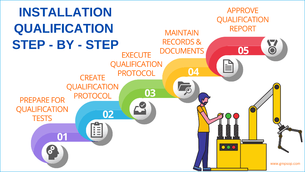
Installation Qualification (IQ) is the documented verification that all equipment, systems, and infrastructure used in medical PCBA manufacturing are installed correctly and conform to approved specifications.
In regulated medical electronics, IQ is not a procedural formality; it is the foundation of process validation.
Before evaluating solder quality, yields, or test results, manufacturers must first prove that the manufacturing environment itself is controlled, traceable, and suitable for medical production. IQ provides this proof in a structured and auditable manner.
Why Is IQ the First Step in Medical PCBA Process Validation?
Medical regulations emphasize process control over end-product inspection. A compliant output cannot compensate for an uncontrolled environment.
IQ is performed first because it:
Establishes baseline manufacturing conditions
Confirms equipment configuration and utilities
Locks approved software and hardware versions
Creates traceable records for future audits
Without IQ, subsequent validation activities such as OQ and PQ lack regulatory credibility.
Which Equipment and Systems Are Included in Medical PCBA IQ?
At Best Technology, IQ for medical PCBA projects typically covers:
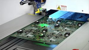
SMT pick-and-place machines, including placement accuracy and software revision
Solder paste printing systems and stencil alignment capability
Reflow and curing ovens, including zone configuration and atmosphere control
AOI, SPI, and X-ray inspection systems
Electrical and functional test platforms
ESD protection infrastructure
MES-based traceability systems
Calibration tools and measurement equipment
Each item is verified against predefined installation requirements, including environmental conditions, utilities, configuration, and calibration status.
Why Is IQ Required for Medical PCBA Compliance?
Medical regulations such as ISO 13485 emphasize process control over final inspection. IQ provides documented proof that the manufacturing environment is controlled, repeatable, and auditable.
IQ is essential because it:
Prevents undocumented equipment substitution
Establishes a validated baseline for audits
Supports long-term traceability for regulated devices
Reduces regulatory risk during design transfer and scale-up
Without IQ, even functional medical PCBAs may be considered non-compliant during audits.
What Are the Risks of Skipping or Weak IQ in Medical PCBA?
Incomplete or missing IQ documentation can lead to:
Audit nonconformities
Delayed supplier qualification
Re-validation requirements
Increased regulatory exposure for OEMs
Even when PCBAs pass electrical testing, lack of IQ can result in formal non-acceptance during audits or regulatory reviews.
How Does Best Technology Implement IQ for Medical PCBA Projects?
Best Technology applies a structured IQ approach that includes:
Approved equipment lists and installation records
Verification of utilities and environmental conditions
Calibration status confirmation
MES and traceability validation
Controlled documentation aligned with medical audits
This ensures a repeatable and defensible foundation for all downstream validation activities.
What is the Relation Between IQ and OQ?
IQ confirms that the manufacturing environment is correctly installed, but it does not validate process performance. Once installation is confirmed, manufacturers must demonstrate that assembly processes operate reliably within defined limits. This is achieved through Operational Qualification (OQ).
In medical PCBA (Printed Circuit Board Assembly), IQ, OQ, and PQ are not procedural formalities; they are foundational controls that directly support patient safety, regulatory compliance, and long-term product reliability. Together, they form a structured validation framework required by global medical regulations and expected by auditors, OEMs, and notified bodies.
Regulatory Compliance Is Not Optional in Medical PCBA
Medical electronic assemblies fall under strict regulatory frameworks such as ISO 13485, FDA 21 CFR Part 820, and EU MDR. These regulations explicitly require manufacturers to validate production processes, not merely inspect finished products.
IQ, OQ, and PQ collectively demonstrate that:
The manufacturing environment is suitable
The process is capable and controlled
The output is consistently compliant
Without documented IQ/OQ/PQ evidence, a medical PCBA supplier will fail audits, risk regulatory findings, or cause customer design transfer delays.
IQ (Installation Qualification): Proving the Factory Is Correctly Set Up
IQ answers one fundamental question:
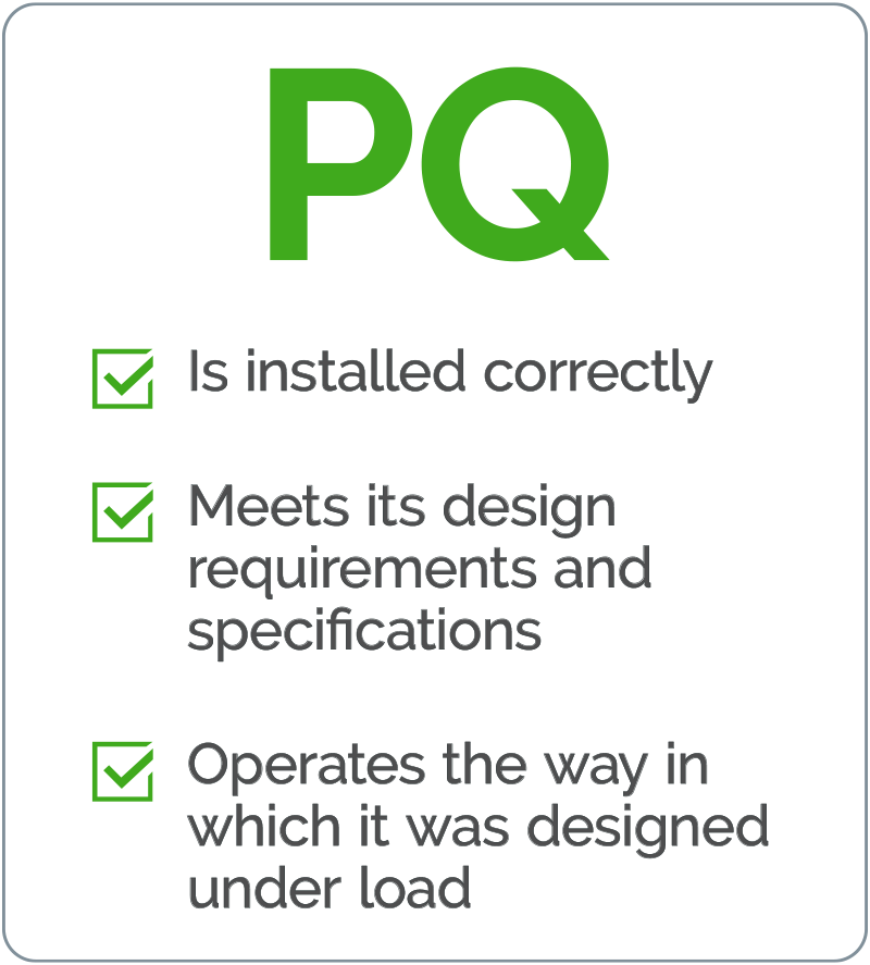
Is the equipment and infrastructure installed exactly as required?
Can we repeatedly build compliant medical PCBAs under real production conditions?
PQ involves:
Running multiple production lots
Using trained operators
Normal shift conditions (not engineering trials)
Measuring yields, defects, and key quality metrics
Typical PQ evidence includes:
First-pass yield (FPY)
Defect per million (DPMO)
Functional test pass rates
Reliability screening results (as applicable)
Why PQ is critical for medical PCBA programs:
Confirms stability over time, not just once
Supports design transfer from prototype to volume
Reduces field failure risk
Protects OEMs from recalls and liability exposure
For implantable, life-support, or diagnostic devices, PQ is often scrutinized line-by-line during audits.
Risk Reduction and Patient Safety
Medical PCBAs frequently operate in:
Life-critical systems
Continuous-use environments
High-reliability diagnostic platforms
IQ/OQ/PQ validation directly reduces:
Latent solder joint defects
Intermittent electrical failures
Process drift over long production cycles
Human variability in assembly steps
In medical applications, a single uncontrolled process variable can translate into patient harm. Validation converts unknown risks into controlled, documented ones.
OEM Confidence and Long-Term Supply Stability
From a customer perspective, IQ/OQ/PQ:
Shortens supplier qualification timelines
Simplifies regulatory submissions
Enables faster scale-up
Reduces ongoing audit burden
Medical OEMs increasingly select PCBA partners based on validation maturity, not just price or capacity.
A supplier that can present complete IQ/OQ/PQ documentation is signaling long-term manufacturing discipline and regulatory readiness.
Why IQ, OQ, PQ Are Non-Negotiable for Medical PCBA?
In medical PCBA manufacturing:
IQ proves the factory is correctly installed
OQ proves the process is technically capable
PQ proves consistent, real-world performance
Together, they ensure:
Regulatory compliance
Process stability
Product reliability
Patient safety
Medical electronics demand more than “working boards.” They demand validated processes that work every time.
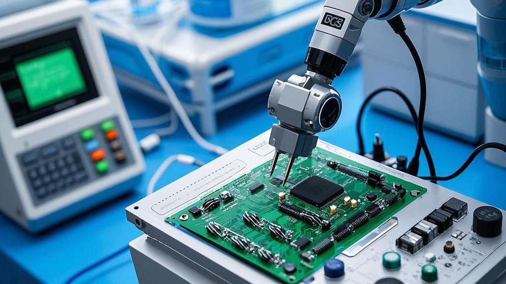
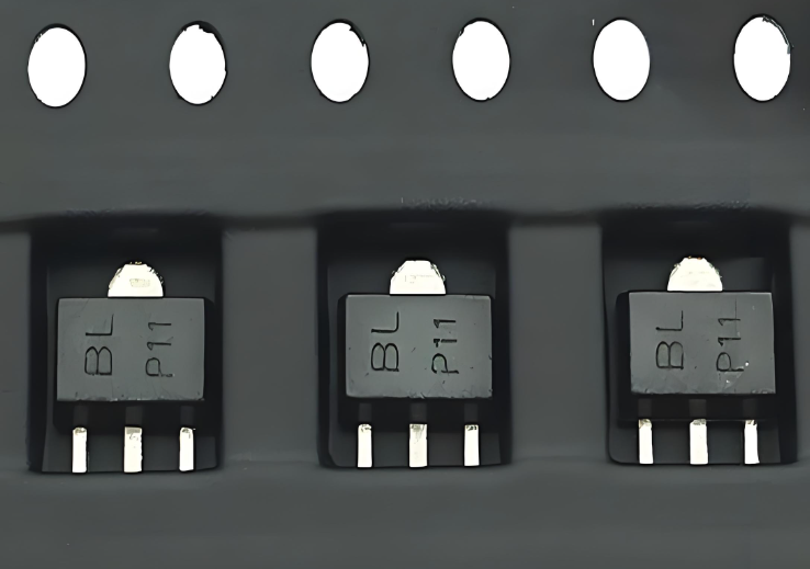
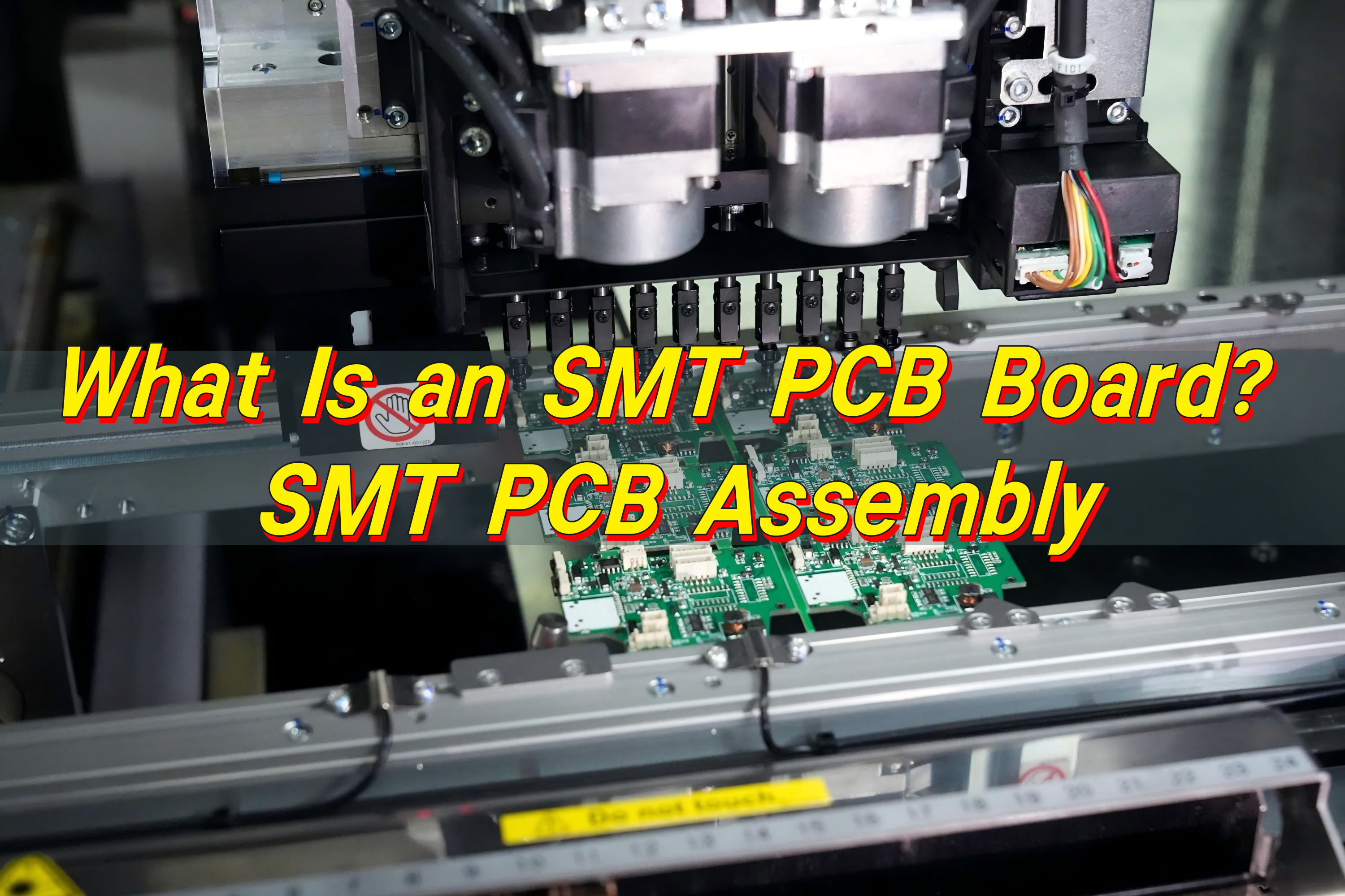
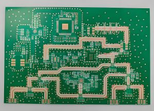
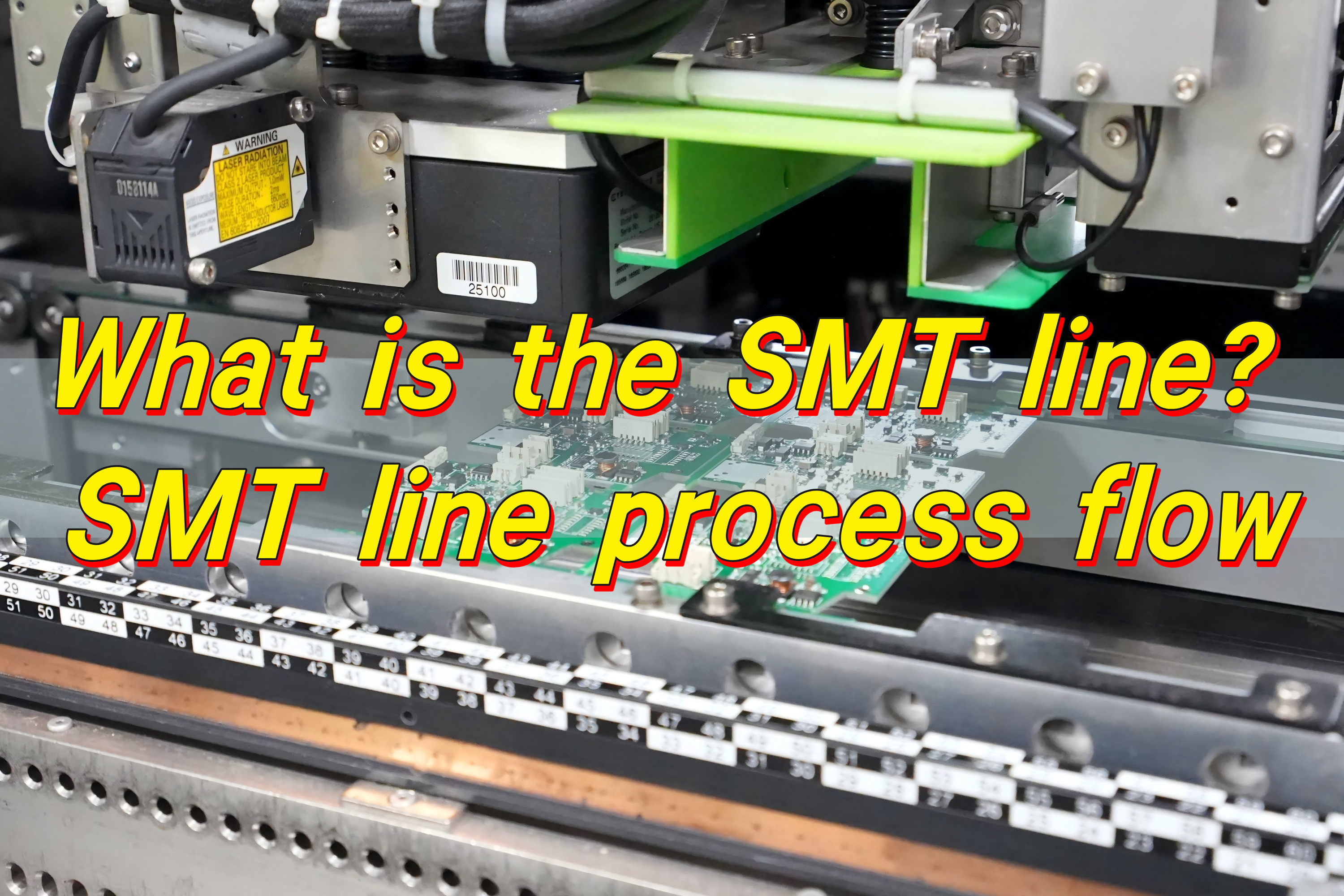
An SMT PCB board is a printed circuit board designed for surface mount technology, where electronic components are mounted directly onto copper pads on the board surface rather than inserted through drilled holes. This approach allows components to sit flat against the PCB, enabling compact layouts, shorter electrical paths, and efficient automated assembly through reflow soldering. As a result, SMT PCB boards support higher component density while maintaining consistent solder quality.
What Is an SMT PCB?
An SMT PCB is a printed circuit board designed specifically for surface mount technology, where electronic components are mounted directly onto copper pads on the surface of the board. Unlike traditional assembly methods, components do not use long wire leads inserted through drilled holes. Instead, they sit flat against the PCB and are soldered in place using controlled reflow processes.
This structural change enables much higher component density. Components can be placed on both sides of the board, and spacing between parts can be significantly reduced. As a result, SMT PCB boards are smaller, lighter, and more electrically efficient than older designs.
Another key benefit is manufacturing consistency. SMT placement is highly automated, allowing machines to position thousands of components per hour with exceptional accuracy. This repeatability improves yield and reduces defect rates, especially in high-volume production.
SMT PCB boards are now standard across consumer electronics, medical equipment, industrial controls, automotive electronics, and communication systems.
How Does SMT Impact PCB Design?
SMT influences PCB design from the earliest layout stage. Because surface-mounted components have short electrical paths, signal integrity improves, especially in high-speed and high-frequency circuits. This allows designers greater flexibility when routing traces and managing impedance.
Pad design becomes a critical factor in SMT layouts. Pad size, shape, and spacing directly affect solder joint quality and long-term reliability. Improper pad geometry can lead to solder bridging, tombstoning, or weak joints, all of which increase rework risk.
Layer stack-up also changes with SMT. Multilayer boards are common, as designers use internal planes for power distribution and noise control. Thermal management becomes more important as well, since compact components can generate localized heat that must be dissipated efficiently.
Finally, SMT PCB design must align with assembly equipment capability. Package size limits, placement tolerances, and inspection access all influence layout decisions.
Is SMT the Same as SMD?
SMT and SMD are closely related terms, but they are not interchangeable. SMT stands for surface mount technology and refers to the manufacturing process used to assemble components onto a PCB. SMD stands for surface mount device and refers to the component itself.
In simple terms, SMT is the method, while SMD is the part. Factories use SMT processes to place SMD components onto SMT PCB boards.
What Is the Difference Between SMD and SMT PCB?
An SMT PCB describes both the board design and the assembly method, while an SMD describes only the component package. SMT PCBs are designed with specific land patterns that support surface-mounted components and reflow soldering processes.
SMD components include chip resistors, capacitors, integrated circuits, and discrete semiconductors packaged for surface mounting. Without an SMT-compatible PCB, SMD components cannot be properly assembled or soldered.
In practice, SMT PCBs and SMD components always work together, but their roles are distinct.
How Does PCB Board SMT Differ From Through-Hole Assembly?
The difference between SMT and through-hole assembly is structural and operational. Through-hole assembly uses drilled holes where component leads pass through the board and are soldered on the opposite side. SMT places components directly onto surface pads without penetrating the board.
SMT enables much higher component density and allows assembly on both sides of the PCB. This supports smaller board sizes and more complex functionality. Through-hole assembly, while mechanically robust, occupies more space and limits layout flexibility.
SMT also supports full automation, while through-hole assembly often requires manual or semi-automated steps. This difference has a significant impact on cost and scalability. However, some products use both methods together, such as board assembly SMT DIP PCB or board assembly SMT THT PCB designs, where connectors or power components still benefit from through-hole strength.
What Is the Major Advantage of Using SMT?
The primary advantage of SMT PCB assembly is efficiency at scale. Automated placement machines operate at high speed with consistent accuracy, enabling reliable mass production. This efficiency directly reduces assembly time and labor costs.
SMT also supports miniaturization. More functionality fits into less space, enabling thinner, lighter, and more portable devices. Electrical performance improves as well, since shorter lead lengths reduce parasitic effects and signal noise.
Reliability benefits from controlled soldering processes. Reflow soldering produces uniform joints, reducing variation and long-term failure risk.
What Components Are Used in SMT?
SMT supports a wide range of electronic components. Common passive parts include chip resistors and capacitors in standardized package sizes. Integrated circuits appear in formats such as SOIC, QFP, QFN, and BGA, supporting everything from simple logic to advanced processors.
Discrete components like diodes, transistors, and MOSFETs are widely used in SMT designs. Many connectors and RF modules are also available in surface-mount packages, allowing compact system integration.
Each component type requires proper footprint design, accurate stencil thickness, and precise placement to ensure reliable solder joints. Successful SMT PCB assembly depends on matching component selection with process capability.
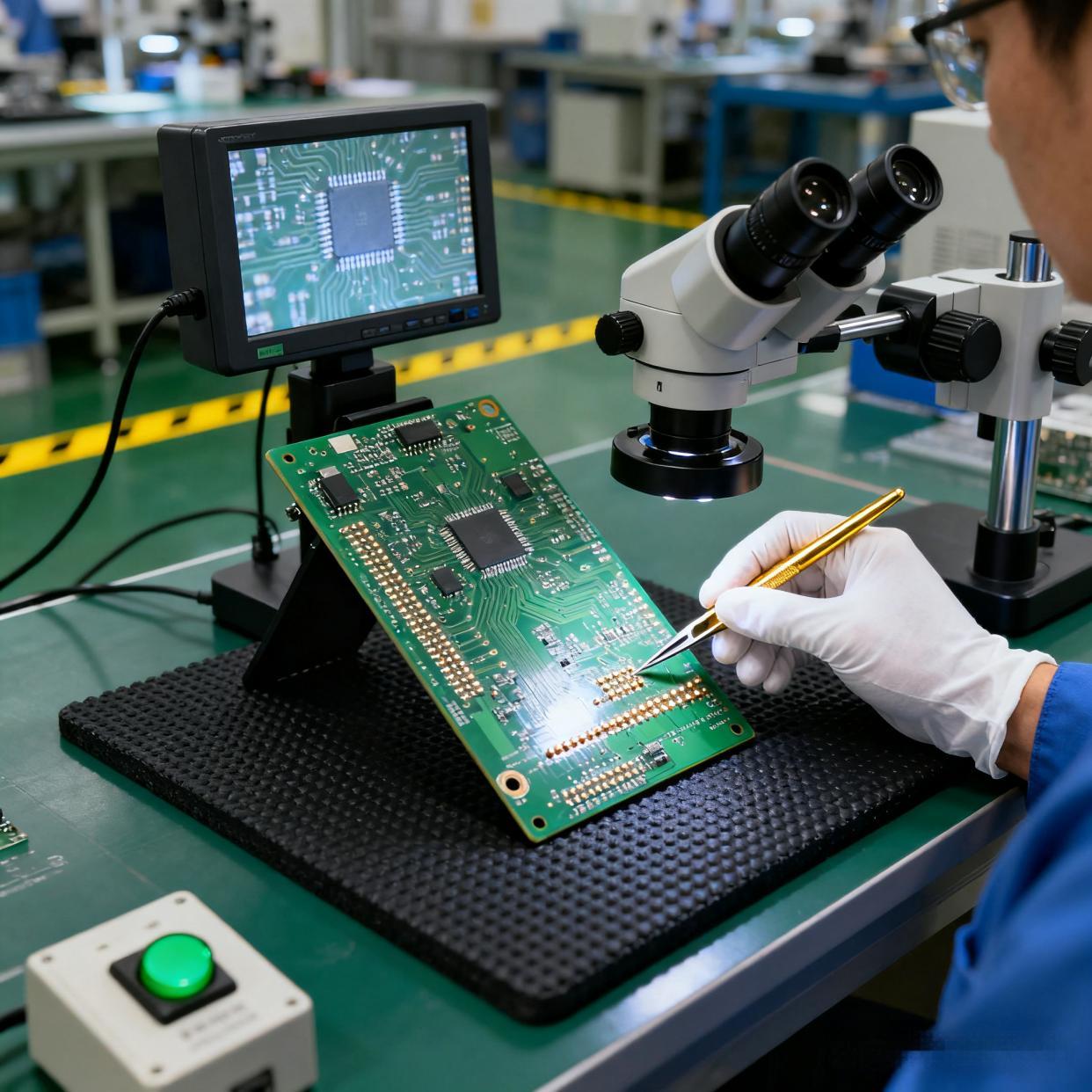
What Quality Checks Are Used in SMT PCB Assembly?
Quality control is central to SMT PCB assembly. Inspection begins with solder paste application, where volume and alignment are monitored to prevent downstream defects. Automated optical inspection then verifies component placement and visible solder joints.
For components with hidden connections, such as BGAs, X-ray inspection is used to evaluate internal solder quality. Reflow temperature profiles are carefully controlled to avoid thermal damage or weak joints.
Electrical testing confirms circuit continuity and functionality, while final inspection ensures cleanliness and cosmetic quality. These layered quality checks protect product reliability and customer confidence.
Where Do We Use SMT?
SMT is used across nearly every electronics sector. Consumer electronics rely on it for compact form factors and high functionality. Industrial and medical devices depend on SMT for precision, consistency, and long-term reliability.
Automotive electronics use SMT for control units and sensor systems that must withstand harsh conditions. Telecommunications and networking equipment rely on SMT to support high-speed signal performance and dense layouts.
As electronics continue to evolve, SMT PCB assembly remains a foundational technology enabling innovation at scale.
Conclusion:
An SMT PCB board is a circuit board built for surface mount technology, where components are placed on surface pads and soldered by reflow for fast, repeatable production. Compared with through-hole assembly, SMT PCB assembly supports higher density, smaller products, and strong electrical performance, which is why it dominates modern electronics.
To learn more about how Best Technology supports these SMT PCB assembly technologies, please contact us at sales@bestpcbs.com
Soldering remains one of the most fundamental operations in electronics manufacturing, and its reliability depends on far more than just heat and solder alloy. Flux is a quiet but powerful material that determines how well a solder joint forms, how stable the connection remains over time, and how durable a finished PCB assembly will be in the field.
For new engineers, technicians, and even seasoned designers, misunderstandings about flux are common—especially around topics such as electrical conductivity, residue behavior, and flux selection for different soldering environments. This guide provides a detailed but easy-to-read explanation of what flux is, what it does, and whether it conducts electricity. It also highlights practical considerations for real PCB assembly workflows.
What Is Flux in Soldering?
Flux is a chemical agent applied during soldering to prepare metal surfaces and support the formation of reliable solder joints. When copper pads or component leads are exposed to air, oxidation naturally occurs. Even a microscopic layer of oxidation can obstruct solder wetting, causing poor joints, voids, and insufficient fillets.
Flux removes these oxides, shields the surface from further oxidation during heating, and helps molten solder spread smoothly across metal surfaces. It improves consistency, lowers defect rates, and stabilizes the soldering process across different alloys and temperatures.
In PCB assembly—whether reflow, wave soldering, or selective soldering—flux is as essential as the solder itself. Without it, joints would frequently fail, especially on components with small contact areas or on boards that require high-density interconnects.
Is Flux the Same as Solder?
Flux and solder are very different materials, even though both are packaged together in solder wire or solder paste.
Solder is a metal alloy that melts and forms the electrical and mechanical connection.
Flux is a chemical compound that prepares the surface and improves the solder’s ability to bond.
Flux does not create a joint by itself. It does not replace the solder alloy. Instead, it ensures the solder achieves a strong, durable bond with copper pads and component leads.
During soldering, flux activates first. As heating continues, solder alloy becomes molten and flows into the prepared surface, producing a joint that is structurally sound and electrically stable.
What Is Flux Made Of?
Flux formulations differ depending on application, activity level, and cleaning requirements, but most contain three major components:
1. Base Material
This forms the bulk of the flux. Common bases include:
Rosin (natural resin from pine trees)
Synthetic resin
Organic acids
Water-soluble organic compounds
2. Activators
These compounds remove oxides and enable solder wetting. Examples include:
Halides and halogen-free activators
Organic acids
Amines
Activators determine how aggressive the flux is and directly influence cleaning requirements.
3. Solvents
Liquids that adjust viscosity and allow the flux to spread evenly. Depending on the type, the solvent may be:
Alcohol-based
Water-based
Mixed solvent systems
Additional additives control stability, residue appearance, heat resistance, and spread behavior.
In solder paste, flux is blended with metal powder (tin-based alloy particles). In liquid or pen flux, the chemical composition varies more widely depending on the intended soldering method.
Types of Flux Used in Electronics Soldering
Flux comes in multiple varieties because different electronic assemblies require different performance and cleaning levels.
1. Rosin Flux (R, RMA, RA)
A classic formulation used for decades.
R (Rosin): Mild, minimal activity
RMA (Rosin Mildly Activated): Balanced activity and reliability
RA (Rosin Activated): Strong oxide removal; requires cleaning
Rosin residues are typically hard and non-corrosive but still benefit from cleaning in sensitive electronics.
2. No-Clean Flux
Designed to leave minimal residue that remains safe on the board.
Very low activity
Ideal for high-volume consumer products
Popular in SMT reflow
However, no-clean flux is not “no-clean” for everything. High-reliability sectors such as medical, aerospace, and automotive often still require cleaning.
3. Water-Soluble Flux
It is a strong, highly active flux. It can:
Removes heavy oxidation
Excellent wetting performance
Residue is conductive and must be cleaned with water
This flux is common for BGA, QFN, and fine-pitch applications due to its high activity.
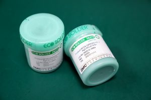
4. Flux Paste, Gel, Liquid, and Pen Types
Each soldering method favors a different form:
Flux paste: Hand soldering, rework
Liquid flux: Wave soldering and selective solder
Gel flux: BGA sphere attachment and reballing
Flux pens: Small-area touch-ups
Choosing the right format ensures controlled application and stable process quality.
What Are the Functions of Flux in Soldering?
The main active component in the soldering agent is rosin. Rosin will be decomposed by tin at around 260 degrees Celsius. Therefore, the temperature of the soldering bath should not be too high. In soldering, it is an indispensable auxiliary material and plays an extremely important role.
Removes surface oxides from copper pads and component leads.
Prevents re-oxidation during heating.
Improves solder wetting, allowing the alloy to spread uniformly.
Reduces surface tension, enabling smoother flow.
Promotes mechanical strength, making joints more reliable.
This combination ensures repeatable and stable solder connections for both prototype and mass production builds.
Is Flux Conductive?
Fresh flux and properly cleaned flux residue are not conductive. Most fluxes are designed to be electrically insulating, even when left on the PCB after reflow or hand soldering.
This is why no-clean flux can remain on many consumer-grade boards without impacting function.
Why Some Flux Residues Become Slightly Conductive?
Although flux itself is non-conductive, residue can become slightly conductive under certain conditions, especially with:
Water-soluble (OA) flux
Highly activated flux
Flux that absorbs humidity over time
Ionic contamination left behind after incomplete cleaning
This moisture-dependent conductivity may cause leakage paths, corrosion, or unpredictable behavior in sensitive analog, RF, or high-impedance circuits. That is why aerospace, medical, and automotive assemblies often require a thorough post-cleaning process.
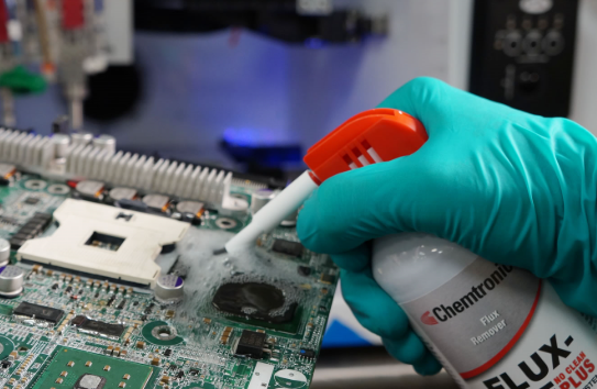
Best Cleaning Methods for Flux Residue
Different assemblies require different cleaning approaches, but the goal is always the same: remove unwanted residue without damaging components or altering board performance. Selecting the right method depends on the flux type, the board’s cleanliness requirements, and the equipment available in your production line.
Isopropyl Alcohol (IPA) Wipe or Brush Cleaning
IPA remains one of the simplest and most effective ways to remove rosin-based flux. A soft brush or lint-free wipe helps dissolve residue quickly, making it ideal for rework, repair, or small-batch builds.
Precision Flux Remover Sprays
Engineers often choose specialized flux remover sprays for dense assemblies or harder residues. These solutions penetrate tight spaces under components and evaporate cleanly. They are especially helpful when dealing with no-clean flux that has carbonized during reflow.
DI Water Cleaning for Water-Soluble Flux
Water-soluble (OA) flux requires complete removal because it contains ionic materials. DI water cleaning, either by hand or in an automated system, rinses away these residues effectively.
Ultrasonic Cleaning
For assemblies with fine-pitch packages, BGA components, or complex geometries, ultrasonic cleaning can reach areas traditional brushing cannot. High-frequency waves dislodge residue in hidden spaces. Not all components tolerate ultrasonic energy, so a controlled process is essential.
Common Mistakes When Using Flux
Many soldering issues trace back to improper use of flux. Common mistakes include:
Applying excessive flux, which can trap residue under components
Mixing different flux types in the same process
Using expired flux that has lost its activity
Selecting a flux that does not match the solder alloy or temperature profile
Not cleaning when required by the flux classification
A disciplined approach helps avoid rework and enhances long-term reliability.
How to Choose the Right Flux for Your Soldering Process?
Select flux based on your assembly method, product reliability, and cleaning capability:
1. Consider the soldering process
SMT reflow often uses no-clean or RMA flux.
Wave soldering may need higher-activity flux.
Hand soldering typically requires easily reactivated flux pens.
2. Match reliability requirements
High-reliability industries prefer water-soluble flux with full cleaning.
Consumer electronics often adopt no-clean materials.
3. Check board materials and surface finishes
For example, ENIG, OSP, and HASL may react differently to flux activity.
4. Account for reflow temperature
Some fluxes degrade if overheated, reducing wetting efficiency.
FAQs
1.Can you solder without flux?
It is possible but not recommended. Flux ensures strong wetting and consistent joints.
2. Is no-clean flux truly “no clean”?
In most consumer applications, yes. For high-reliability products, cleaning may still be required.
3. Does flux expire?
Yes. Its activity decreases over time, which affects soldering quality.
4. Is flux harmful to PCBs?
Not when used correctly. Incorrect cleaning or high-activity residues may cause long-term issues.
5. Why does flux smoke during soldering?
Flux evaporates and burns off as it activates. This is normal.
6. Which flux is best for sensitive electronics?
Low-residue no-clean flux or water-soluble flux with full cleaning.
A cold solder joint is one of the most common failure mechanisms in electronics assembly, yet many technicians and engineers encounter it long before fully understanding its root behaviors. When a joint lacks proper heat, does not wet the copper pad, or cools in an uncontrolled manner, the resulting connection becomes unstable. It may pass initial testing, but its long-term reliability declines.
Because modern electronics demand consistent performance—whether in consumer devices, industrial controllers, automotive modules, or medical PCB assemblies—recognizing and preventing cold solder joints remains essential for every design or manufacturing team.
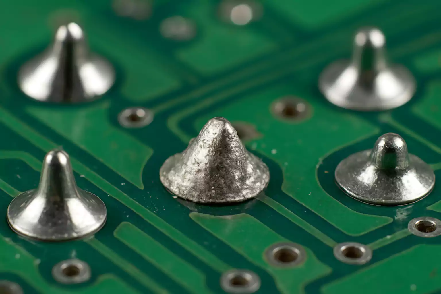
What Is a Cold Solder Joint?
A cold solder joint is a solder connection that forms without reaching the proper temperature for the solder alloy to fully melt, flow, and wet the surfaces. Instead of a smooth, solidly bonded joint, the resulting structure becomes dull, grainy, or cracked. The term “cold” comes from the fact that these joints never reach the temperature required to create a metallurgical bond between the solder and the copper pad or component lead.
In practical terms, the solder solidifies before forming a stable interface. Instead of integrating with the metals it is meant to join, it merely sits on top of the surfaces. The joint may appear attached, but internally it lacks the uniform crystalline structure that defines a reliable connection.
In manual soldering, cold joints often happen due to inconsistent technique. In automated SMT production, they typically arise from incorrect reflow profiles, insufficient preheat, or contaminated pads that prevent proper wetting. Because of these variables, avoiding cold solder joints requires both strong process control and clean material handling.
Do Cold Solder Joints Still Work?
A cold solder joint may still work, at least at the beginning. This is where confusion begins for many technicians. The joint may pass functional testing, power-on checks, or a quick continuity test. Because the mechanical bond is weak and the electrical interface incomplete, the behavior becomes intermittent.
A device with cold joints may operate well in a static environment but become unstable when exposed to:
Temperature swings
Vibration or shock
Thermal expansion during operation
Humidity or oxidation
Long-term cycling
While a cold joint can conduct current, it does so inconsistently, and usually with higher resistance. Over time, micro-cracks grow, creating open circuits or signal noise. For that reason, cold solder joints are considered functional only by coincidence, not by design.
Cold Solder Joint Symptoms
Cold solder joints have predictable symptoms. Engineers often rely on these visual or electrical clues to locate the root cause of a circuit failure:
Dull, Frosty, or Grainy Surface
Irregular Shape or Incomplete Wetting
Visible Cracks or Rings
Intermittent Performance
Increased Resistance
Movement When Touched
Failure Under Thermal Stress
These symptoms are reliable indicators during repair, inspection, or failure analysis.
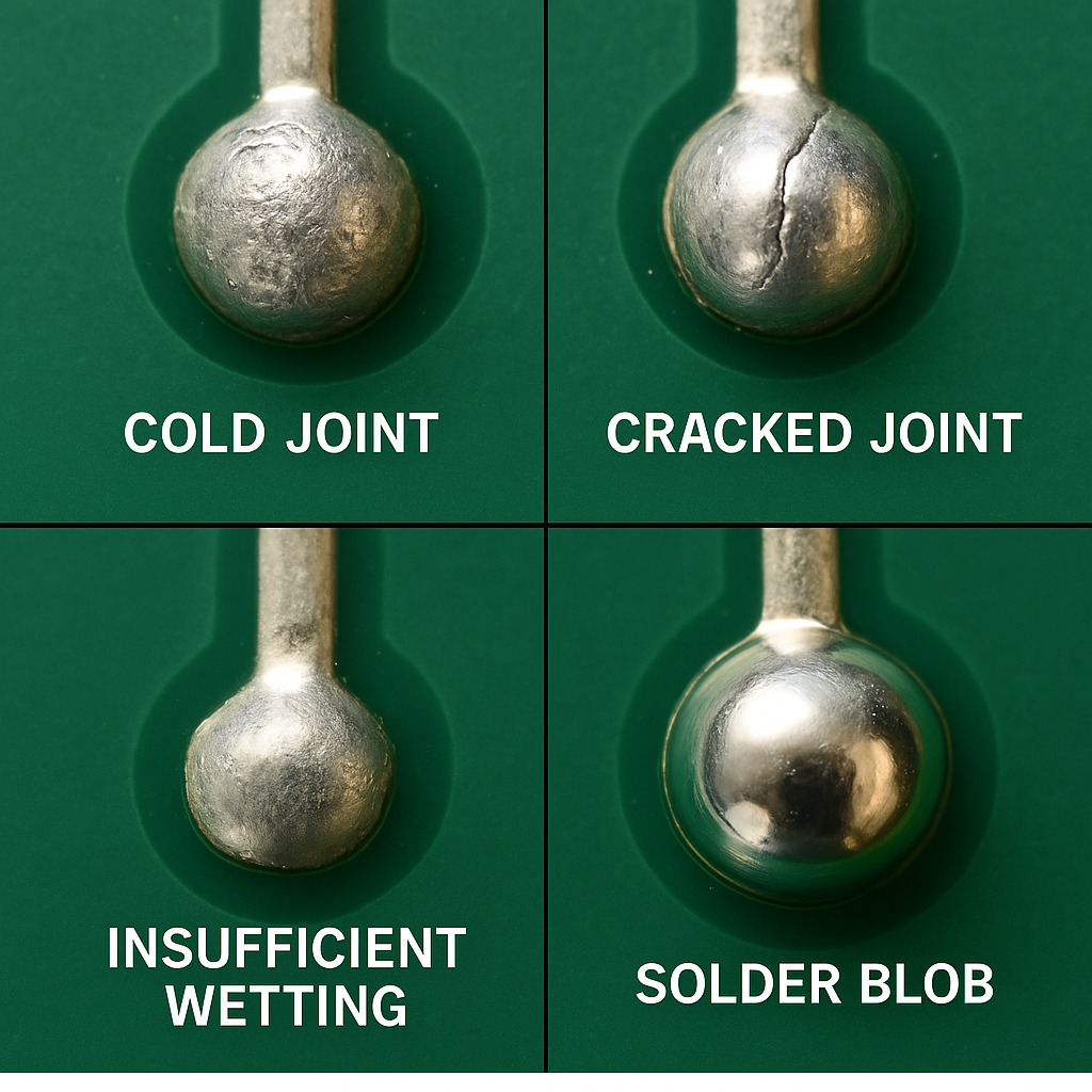
What Is the Difference Between a Cold Solder Joint and a Good Solder Joint?
A good solder joint forms a solid intermetallic bond between the solder, the copper pad, and the component lead. It exhibits a smooth, shiny, and uniform shape with complete wetting.
Comparing both joints helps clarify the contrast:
Aspect
Cold Solder Joint
Good Solder Joint
Appearance
Dull, grainy, frosty surface
Smooth, shiny, uniform surface
Wetting Behavior
Poor wetting; solder sits on top of pad/lead
Complete wetting across pad and lead
Mechanical Strength
Weak bond; prone to cracking or movement
Strong bond with stable mechanical support
Electrical Performance
Higher resistance; intermittent continuity
Low resistance; stable, consistent conductivity
Reliability
Unpredictable; often fails under vibration or heat
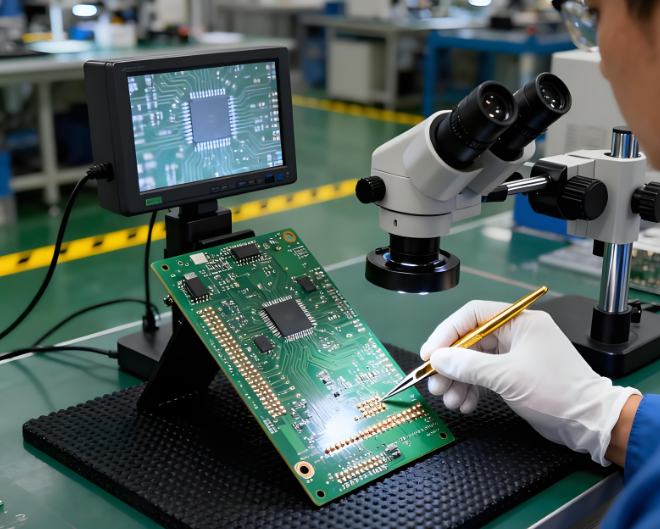
Identifying cold solder joints requires a combination of visual inspection, tactile testing, and electrical measurement. Here are the most common methods:
Visual Inspection
Under a microscope or magnifying lamp, look for dull surfaces, cracks, uneven shapes, or insufficient solder spread. Most cold joints are visible to a trained eye.
Continuity and Resistance Testing
Using a multimeter, check whether current flows consistently. Cold joints may pass continuity tests but show higher resistance.
Thermal Stress Testing
Heating or cooling the PCB may cause the joint to open or reconnect.
X-ray Inspection (for BGA or QFN)
In high-density packages, internal cold joints appear as voids, incomplete wetting, or irregular solder shapes.
Mechanical Movement
Applying gentle pressure can reveal looseness in through-hole components.
Early identification is essential in avoiding expensive rework or device failure.
Are Cold Joints Acceptable?
Cold solder joints are not acceptable in any professional electronics assembly environment. Industry standards such as IPC-A-610 define cold joints as defects requiring correction. Even in hobby projects, cold joints degrade reliability.
There are no scenarios where cold joints are intentionally tolerated. Any sign of incomplete wetting or insufficient flow must be corrected immediately. or mission-critical industries such as:
Medical
Automotive
Industrial automation
Aerospace
IoT
Telecommunications
cold solder joints represent unacceptable risk.
What Causes a Cold Solder Joint?
Cold solder joints form due to several common process issues. Understanding these causes helps prevent recurrence.
1. Insufficient Heat
If the soldering iron does not fully heat the pad and lead, wetting cannot occur.
2. Contaminated or Oxidized Surfaces
Residue, dust, oxide layers, or aged plating can block wetting.
3. Incorrect Solder Alloy or Temperature
Low heat settings, mismatched solder types, or incorrect thermal profiles lead to poor flow.
4. Poor Flux Activity
Flux cleans surfaces. Weak or expired flux prevents proper bonding.
5. Movement During Solidification
If the lead moves before the solder cools, a cold joint forms.
6. Inconsistent Reflow Profile
In SMT production, a poorly tuned reflow oven produces cold joints, especially on large thermal pads or ground planes.
7. Manual Soldering Technique Errors
Rushed or inconsistent soldering practices can create joints that never heat sufficiently.
1. The device may work partially, only under specific temperature or vibration conditions.
2. Higher resistance destabilizes signals, especially in RF or high-speed digital designs.
3. Poor conductivity forces current to generate heat, stressing components.
4. Cold joints often degrade quickly in real-world conditions.
5. In power electronics, cold joints increase the risk of arcing or thermal runaway.
These risks emphasize the need for controlled soldering conditions, proper inspection, and strict quality assurance.
How to Avoid Cold Solder Joints?
Preventing cold solder joints requires strong process management, skilled operators, and adherence to IPC and manufacturer guidelines.
1. Ensure Proper Heating
Heat both pad and lead evenly. Maintain appropriate soldering temperatures for the chosen alloy.
2. Use High-Quality Solder and Fresh Flux
Materials is important, Fresh flux ensures clean surfaces and stable wetting.
3. Clean and Prepare Surfaces
Remove oxidation, oil, or contamination before soldering.
4. Maintain Stable Reflow Profiles
For SMT production, program time-temperature profiles to match the alloy. Adjust for heavy copper or large thermal pads.
5. Avoid Movement During Cooling
Secure components so solder can solidify without vibration.
6. Use Proper Tools
ESD-safe irons, clean tips, good tweezers, and inspection magnification help ensure accuracy.
7. Follow IPC Guidelines
Standards such as IPC-A-610 and IPC-J-STD-001 provide industry-accepted criteria for solder quality.
Understanding the distinction between a cold solder joint and a properly formed one helps engineers and technicians diagnose failures accurately. A cold solder joint appears dull, weak, and inconsistent, while a good joint is smooth, shiny, and electrically stable. The difference directly affects device performance and lifespan.
As electronics continue shrinking and integrating more complex components, the need for reliable soldering becomes even more critical. Whether you are working with prototype boards, high-density PCBs, or mission-critical assemblies, eliminating cold joints should always be a priority.
A cold solder joint is one of the most common reliability defects in PCB and PCBA assemblies, and it continues to be a major source of intermittent failures across consumer electronics, industrial controls, medical devices, automotive modules, and aerospace hardware. At Best Technology, we see the long-term consequences of cold joints in incoming failure analyses from global customers—especially in assemblies where stable conductivity and mechanical strength are critical.
With 19 years of PCBA production experience across China and Vietnam, medical-grade and aerospace-grade certifications, and MES-controlled SMT lines, we understand how cold solder joints emerge, how to eliminate them, and how to engineer assemblies that remain stable throughout the product life cycle.
What Is a Cold Solder Joint?
A cold solder joint forms when solder does not melt or wet the pad and component lead completely. Instead of creating a unified bond, the solder cools prematurely or never flows correctly, resulting in a dull, grainy, or uneven connection.
In the PCBA environment, cold joints are considered a process defect because they weaken the mechanical integrity of a soldered connection and create unstable electrical performance that deteriorates over time.
In high-reliability sectors—medical, industrial, aerospace—these defects are unacceptable and must be removed at the root cause: temperature control, surface condition, solder alloy behavior, and wetting characteristics.
Do Cold Solder Joints Still Work?
Temporarily, yes. Reliably, no. A cold solder joint may appear functional during a quick test, then fail:
When the board heats during normal operation
When vibration or slight mechanical stress occurs
When humidity or temperature cycles change contact resistance
When current load increases
This unstable behavior is what makes cold joints one of the most misdiagnosed failure sources. Many customers approach Best Technology believing they have a “component issue” or “firmware bug,” when the real cause is inconsistent solder metallurgy.
Cold Solder Joint Symptoms
From a PCBA viewpoint, cold joints create early-life failures that escalate under stress. Common symptoms include:
Intermittent booting or power instability
Flickering LEDs, displays, or inconsistent sensor readings
Weak or noisy signals in communication lines
Overheating around a soldered component
Boards that only work when pressed or tapped
Modules that behave differently under temperature changes
During incoming quality analysis at Best Technology, we often find that unstable BGA balls, hand-soldered connectors, and TH pins are common locations for cold joints.
What Is the Difference Between a Cold Solder Joint and a Good Solder Joint?
A good solder joint creates a smooth, bright, and uniform connection that wraps around the lead with full wetting.
A cold joint typically shows:
A dull or matte finish
Crystalline or grainy texture
A ring fracture around the lead
A small gap between solder and pad
Solder balled up instead of flowing
Experienced technicians immediately recognize these visual cues because they suggest weak mechanical support and unstable electrical conductivity.
How to Identify a Cold Solder Joint?
Both technicians and advanced PCBA factories rely on a few inspection methods:
Bright-light and angled inspection to reveal dull or frosted surfaces
Magnification to highlight cracks or gaps
Gentle mechanical pressure to detect movement
Thermal testing to expose resistance changes under heat
AOI or X-ray for lead-free and hidden joints
In Best Technology’s MES-controlled lines, each soldering step—including reflow, wave, and selective solder—is tied to traceable profiles, making it easier to isolate and prevent cold joints during future builds.
Are Cold Joints Acceptable?
No. Cold solder joints are never acceptable in professional electronics.
They violate:
IPC-A-610 standards
Reliability requirements
Safety and quality regulations
Even in low-cost consumer electronics, cold joints significantly reduce product lifespan and reliability.
What Causes a Cold Solder Joint?
Cold solder joints originate from several process-related or operator-related factors:
Insufficient soldering temperature
Iron tip or nozzle unable to deliver stable heat
Oxidized pads, leads, or old components
Expired or poorly stored solder paste
Flux burnout or inadequate flux coating
Component movement during cooling
Large copper areas absorbing heat too fast
Incorrect reflow curve in SMT production
With our dual factories in China and Vietnam, Best Technology maintains strict humidity control, paste storage, stencil management, and reflow calibration—reducing these risks dramatically.
In medical, industrial, and aerospace PCBAs, even a single cold joint is considered a critical defect (CD level). Best Technology screens aggressively to ensure these defects never leave the factory.
How to Fix a Cold Solder Joint?
Repair is direct, but must be done properly:
1. Clean the joint with isopropyl alcohol.
2. Apply quality flux to re-activate the surface.
3. Reheat the joint until solder melts fully.
4. Add a small amount of fresh solder if needed.
5. Allow full cooling without movement.
6. Inspect visually to ensure proper fillet and wetting.
For SMD components (QFN, BGA, LGA), reflow or hot-air rework ensures even heating.
How to Avoid Cold Solder Joints?
Prevention stems from controlled process engineering:
Use calibrated, temperature-controlled soldering equipment
Maintain component and PCB cleanliness
Follow correct reflow temperature profiles
Apply flux or paste with proper wetting characteristics
Preheat heavy copper boards
Avoid vibration during cooling
Use AOI/X-ray to verify solder integrity
Enforce operator training and certification
At Best Technology, these practices are embedded into MES workflows, ensuring traceability and repeatability—from prototype to mass production.
FAQ About Cold Solder Joint
1. Can flux prevent cold solder joints?
Flux improves wetting, but without proper temperature, cold joints still occur.
2. Can a cold solder joint cause a short?
Yes. Cracking or partial bonding may create unintended bridges.
3. Why are cold solder joints more common in lead-free solder?
Lead-free alloys require higher melting temperatures and tighter process control.
4. Can a multimeter detect a cold solder joint?
Sometimes, but intermittent faults often remain hidden until the board is heated or flexed.
5. Can reheating permanently fix a cold solder joint?
If the pad and lead are clean and properly wetted, reheating provides a permanent repair.
6. Do professional PCBA manufacturers still encounter cold joints?
Rarely, but only because inspection systems, controlled processes, and trained operators keep solder quality consistent.
When to Consult a Professional or a PCBA Manufacturer?
If your board shows repeated failures, unstable behavior, or numerous questionable joints, professional evaluation is the safest choice. Best Technology supports global customers with:
In-house FA (failure analysis)
X-ray and AOI inspection
Controlled reflow soldering
Medical-grade and aerospace-grade quality systems
MES-tracked production across China and Vietnam
Whether you need prototype repair, DFX recommendations, or full PCBA manufacturing, our engineering teams ensure solder reliability at every stage of the product life cycle.
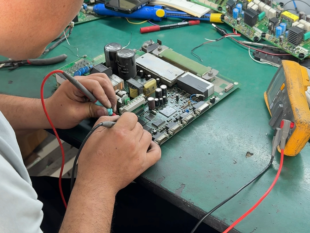
How to test electronic circuit board? Testing an electronic circuit board is a critical step to ensure functionality, reliability, and safety before mass production or deployment. A well-structured testing process helps identify design flaws, assembly defects, and component failures early—saving both time and cost.
How to Test an Electronic Circuit Board?
To begin, place the board on a stable surface with proper lighting. Before you touch anything, disconnect all power sources.
Next, perform a visual inspection. This simple act often reveals more information than expected. Look for burned areas, cracked components, lifted pads, poor solder joints, or debris. A magnifying lamp makes this process easier.
After the visual check, inspect connectors, jumpers, and wires. Loose connections appear harmless but often create intermittent issues that feel impossible to catch. A light touch with tweezers confirms stability.
Once the board passes the visual stage, move to electrical testing. A multimeter becomes your most trusted tool. Use continuity mode to confirm that important traces are connected. Use voltage mode to verify that power rails provide stable output. Use resistance mode to track suspicious paths.
During testing. If something feels unusual—temperature differences, unexpected noise, odd smells—pause and investigate.
How to Test Electronic Components on a Circuit Board?
Testing individual components is the next logical step because a PCB is only as reliable as each device mounted on it. When a component fails, it often takes down the entire function.
Start with passive components. Resistors are easy to check using the resistance mode on a multimeter. Measure across both ends. If the value appears close to the labeled rating, the resistor is healthy. If the value is extremely high, open, or inconsistent, it may be faulty.
Capacitors require a different approach. When testing capacitors, use capacitance mode if available. For electrolytic capacitors, check for bulging or leaking material. These symptoms almost always indicate failure. For ceramic capacitors, inspect for cracks. Even hairline cracks can cause unstable behavior.
Next, check diodes. These parts allow current to flow in only one direction. Use diode mode on your multimeter. A healthy diode shows one direction with low forward voltage and the other direction with high resistance. If it shows low resistance in both directions, it is bad.
Transistors require a bit more attention. You can test them using diode mode by checking junction behavior. If the readings do not follow expected patterns, the transistor may be damaged.
Integrated circuits are more complex to test directly. Instead, check their input and output voltages relative to the datasheet. If the IC receives the correct signals but responds incorrectly, it may be faulty.
Sensors, connectors, coils, and switches also deserve inspection. Loose contacts or internal breaks lead to intermittent failures that frustrate even experienced technicians.
How to Test Circuit for Short on Electronic Board?
A short circuit is one of the most common and stressful PCB issues. The good news is that detecting a short is often easier than expected, especially when using the right steps.
Begin by switching your multimeter to continuity mode. Touch one probe to the ground reference. Touch the other to various power points such as 3.3 V, 5 V, or 12 V rails. If you hear a beep, it means there is continuity—possibly a short.
Do not panic if continuity appears at first. Some circuits use intentional low-resistance paths. Instead, look for extremely low resistance, usually near zero ohms. That value often indicates a short.
Move through the board section by section. Check areas where power lines run close to ground. Solder bridges, damaged vias, and misaligned components cause accidental shorts more often than people realize.
If the PCB is multi-layer, you may need to isolate regions by lifting components such as decoupling capacitors. Removing them temporarily helps narrow down the exact node causing trouble.
Thermal cameras, even simple ones, can help detect shockingly fast where the short is hiding. Components sitting on a short path heat up quickly even with tiny amounts of voltage.
How to Test if a Circuit Board Is Bad?
First, observe the power behavior. If the board fails to start or shows unstable voltage, there may be a damaged regulator or short. Use your multimeter to check the rails. Healthy boards deliver stable readings.
Second, examine functionality. Does the board complete its tasks? Do LEDs light as expected? Does the CPU start? Even small symptoms provide big clues. For instance, an LED flickering instead of glowing steadily indicates unstable current or improper grounding.
Next, perform thermal observation. If any component heats too quickly, it may be failing. Healthy boards warm slowly and evenly.
Another sign is physical condition. Bad boards often exhibit damaged traces, cracked solder joints, corrosion, or burnt areas.
Software tools such as oscilloscopes or logic analyzers can also reveal deeper issues. Incorrect waveforms often indicate a bad board even when the components appear intact.
If several tests reveal inconsistent results, or if the board repeatedly fails under mild load, it is likely defective.
How Do I Test a PCB with a Multimeter?
A multimeter is one of the most powerful tools for testing PCBs because it reveals real electrical behavior.
To begin, ensure the multimeter battery is healthy. Weak multimeter power may give misleading readings.
Use the continuity mode to trace connections. This test is simple but effective because it verifies whether the PCB’s paths are intact. Place one probe on one end of a trace and the second at the opposite end. If the multimeter beeps, you confirm electrical continuity.
Use the resistance mode to examine suspicious components. High resistance where there should be low resistance is a warning.
Then use voltage mode on a powered board. Measure power rails to confirm stable output. Move on to test key IC pins. Compare the readings with datasheet requirements. Small deviations may indicate early failures. Larger gaps point to serious issues.
Finally, use current measurement if necessary. This test should be done carefully. Excess current flow usually points to a short or overheating component.
Can You Cut a Circuit Board and It Still Work?
The answer is: yes, a circuit board can still work after cutting, but only under specific conditions.
Cutting a PCB should be done with extreme care. The board will continue working only if you avoid damaging active traces, copper planes, or functional zones. Many PCBs contain dense routing, so a careless cut could destroy the device.
If you must cut a circuit board, examine the board layout first. Look for areas without copper. Many boards intentionally include cut-lines for modular use. These areas are safe to cut as long as you stay within the boundaries.
Use tools designed for PCB cutting such as scoring knives, mills, or board shears. Regular tools may crack the laminate or tear pads.
After cutting, inspect the edges. Smooth them if needed. Ensure no copper is exposed or touching unwanted surfaces.
When done properly, a cut PCB can continue working exactly as before. It depends entirely on how well you prepare and execute the cut.
How to Troubleshoot and Repair Electronic Circuit Boards?
Troubleshooting a PCB is a blend of logic, patience, and methodical thinking. The process begins with clear observation and continues through structured testing until the root problem is solved.
Start with the symptom list. What exactly is the board failing to do?
Next, examine power. In many cases, weak or unstable power is the hidden cause behind strange behavior.
Move on to signal behavior. Use tools like oscilloscopes or logic probes to check timing and waveform integrity. Unexpected waveforms often signal failing components or broken connections.
Then follow a zone-based approach. Break the board into functional regions—power, processing, communication, outputs, and sensors. If you suspect a component, replace one part at a time. Do not replace everything at once.
Reflowing solder joints also saves many boards. Cold joints and cracked pads create intermittent issues that vanish after a clean reflow.
With these methods, troubleshooting and repairing electronic circuit boards will become a predictable process.
Conclusion:
Whether you are checking components, detecting shorts, verifying power rails, testing the board with a multimeter, cutting a PCB safely, or repairing complex circuits, the process becomes manageable when broken into structured steps.
If you need assistance with PCB design, manufacturing, or troubleshooting support, feel free to contact us at sales@bestpcbs.com
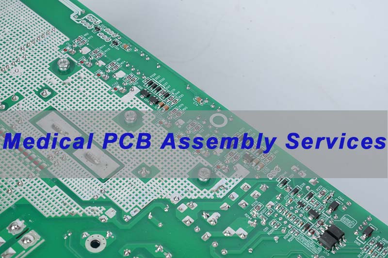
Medical PCB assembly services are the specialized production and system integration of printed circuit boards for life-critical medical equipment. This article explores how partnering with the right provider ensures reliability, compliance, and innovation in healthcare technology.
Developing a new medical device is a high-stakes endeavor. Key Pain Points for Medical Device Developers:
Regulatory Maze: Navigating FDA, ISO 13485, and IEC 60601 standards without expert guidance is time-consuming and risky.
Design for Manufacturing (DFM) Gaps: Prototype designs often have hidden flaws that cause failures during volume production.
Supply Chain Insecurity: Unreliable component sourcing or offshore delays jeopardize project timelines and device availability.
Inconsistent Quality: Lack of rigorous process controls leads to field failures, recalls, and patient safety risks.
Prototype Bottlenecks: Slow turnaround times for design iterations critically delay testing, verification, and time-to-market.
These challenges demand a partner with specialized expertise. The following solutions are foundational to a trusted medical electronics manufacturing relationship.
Proactive Compliance Framework: A partner with ingrained quality systems (ISO 13485 certified) guides you through documentation and validation seamlessly.
Early DFM/DFA Analysis: Expert engineers review designs pre-production to eliminate errors, enhance reliability, and reduce costs.
Controlled, Traceable Supply Chain: Using a vetted network of component suppliers and US based PCB assembly capabilities mitigates shortage and geopolitical risks.
Dedicated Rapid Prototyping Lines: Offering quick turn PCB USA services accelerates the design-test-iterate cycle, getting you to clinical trials faster.
EBest Circuit (Best Technology) is a specialized PCB manufacturing and assembly provider focused on the rigorous demands of the medical sector. Our state-of-the-art facility is ISO 13485:2016 certified, and our global production network includes advanced SMT factories in both China and Vietnam. Each site operates under a unified MES-driven manufacturing system, enabling full process traceability, tighter quality control, and consistent performance across all medical projects. Our engineering team is dedicated to merging technical excellence with regulatory mastery, ensuring every medical PCB meets the highest reliability and compliance standards. For a consultation on your next PCBA printed circuit board assembly project, contact us at sales@bestpcbs.com.
How Do Medical PCB Assembly Services Ensure Reliable Performance in Today’s Healthcare Electronics?
Reliable performance in medical electronics is non-negotiable. Medical PCB assembly services achieve this by implementing a multi-layered approach to quality and control that far exceeds commercial standards.
Medical-Grade Materials & Components: Only using high-Tg laminates, conformal coatings, and components rated for extended life and stable performance in physiological environments.
Enhanced Process Controls: Strict adherence to controlled procedures for soldering (e.g., lead-free SAC305 profiles), cleanliness (ionic contamination testing), and electrostatic discharge (ESD) protection.
Comprehensive Testing Protocol: Every board undergoes a battery of tests:
Test Method
Purpose
Automated Optical Inspection (AOI)
Catches soldering defects, missing, or misaligned components.
X-Ray Inspection
Verifies integrity of BGAs, internal layers, and via fills.
In-Circuit Test (ICT)
Checks electrical performance and component values.
Functional Test (FVT)
Simulates the device’s real-world operation.
Full Traceability: Lot-by-lot and even board-level tracking of all materials and components is maintained, a critical requirement for FDA audits and potential recall actions.
Environmental Stress Screening (ESS): Subjecting boards to thermal cycling and burn-in to identify and eliminate early-life failures (infant mortality).
In summary, reliability is engineered through a combination of superior materials, meticulous processes, and exhaustive verification, ensuring devices perform as intended over their entire service life.
What Is the Difference Between PCB Fab and Assembly?
The journey from design to a functional board involves two distinct, sequential phases: fabrication (PCB fab) and assembly (PCB manufacturing and assembly). Confusing them can lead to project missteps.
PCB Fabrication (Fab): This is the process of manufacturing the bare, unpopulated circuit board. It starts with design files (Gerbers) and involves:
Creating the substrate laminate.
Imaging and etching the copper layers to form traces.
Drilling holes (vias and through-holes).
Applying solder mask and silkscreen.
Performing electrical testing on the bare board.
Output: A bare PCB with pads and holes, ready for components.
PCB Assembly (PCBA): This is the process of mounting and soldering electronic components onto the fabricated bare board. It involves:
Applying solder paste via stencil.
Placing components (Surface-Mount Technology – SMT) using pick-and-place machines.
Reflow soldering to create electrical connections.
Through-hole component insertion and soldering.
Cleaning, inspection, and functional testing.
Output: A fully functional, populated printed circuit board assembly.
Think of PCB fab as printing the wiring diagram and PCB assembly as installing all the light switches, outlets, and fixtures. A true turnkey partner, like a professional PCB design company turned manufacturer, expertly manages both phases.
Why Medical PCB Assembly Services Demand Higher Standards Than Conventional PCB Manufacturing and Assembly?
Medical devices directly impact human life, making failure unacceptable. This fundamental truth elevates every requirement from the component level to the final system integration.
Regulatory Scrutiny: Medical devices require formal approval (FDA, CE). The entire production process must be documented and validated under standards like ISO 13485. A simple process change in conventional manufacturing can become a major, documented change request in medical.
Extreme Reliability & Longevity: A consumer device may have a 2-3 year life. An implantable or critical care device must function flawlessly for 10-15+ years. This demands higher-grade materials and accelerated life testing.
Risk Management (ISO 14971): Every potential failure mode must be identified, analyzed, and controlled. The assembly process itself is a critical control point to mitigate risks like short circuits or cold solder joints.
Biocompatibility & Cleanliness: Devices contacting patients must not leach harmful substances. Assembly processes must ensure extreme cleanliness to avoid ionic contamination that could cause corrosion or failure.
Traceability: While batch traceability might suffice for consumer goods, medical devices often require component-level traceability to facilitate targeted recalls if a supplier’s component batch is found faulty.
Therefore, medical PCB assembly services are not just about soldering components; they are about executing a rigorously controlled, documented, and validated protocol where quality is measured in patient safety outcomes.
How Best Rigid-Flex PCB Assembly Services for Medical Devices Enhance Durability and Miniaturization?
Best rigid-flex pcb assembly services for medical devices unlock innovative form factors by combining rigid boards for component support with flexible circuits for dynamic movement and space savings.
Enhancing Durability:
Reduced Interconnections: Replacing fragile connectors and ribbon cables with soldered flex connections minimizes points of failure.
Vibration/Shock Resistance: The flexible portions absorb and dissipate mechanical stress, protecting solder joints.
Improved Reliability: A monolithic rigid-flex structure is more reliable than an assembly of multiple interconnected rigid boards.
Enabling Miniaturization & Wearability:
3D Packaging: Boards can be folded into compact, three-dimensional shapes, crucial for implants, hearing aids, and endoscopic capsules.
Weight Reduction: Eliminating connectors and using thin flex layers reduces overall weight—key for portable and wearable monitors.
Dynamic Flexing: Allows for designs in hinged devices or probes that require repeated movement.
For a factory wholesale medical PCB assembly service, mastering rigid-flex is a key capability. It requires specialized PCB fab expertise for multilayer bonding and precise PCB assembly techniques to handle the delicate flex areas during soldering and handling.
Capabilities of a US Based PCB Assembly Partner for Healthcare OEMs
A US based PCB assembly partner provides a mature infrastructure, advanced engineering support, and tightly controlled manufacturing systems tailored for the demanding needs of Healthcare OEMs.
Advanced Engineering Collaboration Localized teams provide rapid design reviews, DFM/DFA optimization, and direct engineering communication that shortens development cycles and reduces risk before prototypes are built.
Highly Controlled Manufacturing Processes U.S. facilities apply strict process validation, IPC Class 3 manufacturing, real-time monitoring, and data-driven production oversight aligned with FDA and ISO 13485 expectations.
Robust Traceability and Documentation Systems MES-based traceability, controlled documentation, and production records tailored for medical audits support DHF/DMR requirements and simplify compliance workflows.
Reliable Quick-Turn Prototyping and Small-Batch Production Domestic fabrication and assembly resources enable consistent quick turn PCB USA results, accelerating verification testing and early clinical evaluations.
Secure and Verified Supply Chain U.S. partners maintain qualified suppliers, validated sourcing protocols, and controlled inventory management to support long-term availability and stable BOM planning.
Specialized Medical Manufacturing Expertise Experienced operators, medically trained technicians, and quality teams understand the expectations of Healthcare OEMs—from cleanliness requirements to test coverage and failure analysis.
A US based PCB assembly partner is not merely a vendor—it is a capability-driven extension of your R&D and manufacturing team, providing the technical depth, control, and confidence required for regulated medical devices.
How a Professional PCB Design Company Supports Medical Product Development from Concept to Verification?
A professional PCB design company is a vital co-pilot, transforming a conceptual medical device into a manufacturable, reliable, and certifiable product.
Concept & Architecture: Advises on system partitioning, component selection, and technology (e.g., rigid-flex) to meet size, power, and cost targets.
Schematic Capture & Simulation: Creates the electrical blueprint and runs signal/power integrity simulations to prevent performance issues.
PCB Layout with DFM/DFA Rules: Engineers the physical board layout with strict adherence to medical-grade spacing, high-reliability routing, and, crucially, Design for Manufacturing/Assembly rules from the start.
Design for Test (DFT): Incorporates test points and features to ensure the assembled board can be thoroughly validated.
Documentation for Compliance: Generates the complete design history file (DHF) output needed for regulatory submission, including schematics, layouts, BOMs, and design rationale.
Support through Verification & Validation (V&V): Works with the assembly partner to troubleshoot prototype builds and provide design revisions.
This end-to-end support de-risks development, ensuring the design is optimized not just for function, but for manufacturability and compliance from day one.
Why Many Healthcare Startups Seek Quick Turn PCB USA Solutions for Prototype Acceleration?
For healthcare startups, speed to proof-of-concept and clinical validation is critical for funding and market entry. Quick turn PCB USA services are the engine for this acceleration.
Rapid Design Iteration: Fast prototype turns (e.g., 24-72 hours for fab, 5-10 days for assembly) allow engineers to test, discover flaws, and refine designs in quick succession.
Faster Clinical & Regulatory Milestones: Functional prototypes are needed for benchtop testing, animal studies, and human trials. Faster builds compress the overall development timeline.
Cost-Effective Exploration: Enables affordable testing of multiple design approaches or form factors before locking in final tooling for volume production.
Attracting Investment: A working, refined prototype is far more compelling to investors than just a CAD model or idea.
By leveraging domestic quick turn PCB USA capabilities, startups maintain agility and momentum, turning innovative ideas into tangible devices with exceptional speed.
How Can a Factory Wholesale Medical PCB Assembly Service Ensure Consistent Quality and Compliance for Regulated Healthcare Devices?
A true factory wholesale medical PCB assembly service achieves consistent quality not through luck, but through a systemic, process-oriented approach built for the medical industry.
Certified Quality Management System (QMS): Operation under ISO 13485:2016 is not optional; it’s the foundational framework that ensures consistent processes, corrective actions, and management oversight.
Standardized Work Instructions & Process Validation: Every assembly step is defined, documented, and validated to prove it consistently produces a result meeting pre-defined specifications.
Advanced Process Control & Monitoring: Solder paste inspection (SPI), automated optical inspection (AOI), and real-time thermal profiling of reflow ovens catch deviations in real-time.
Rigorous Supplier Management: Components are sourced from approved vendors with full lot traceability. Incoming materials are inspected and certified.
Independent Quality Assurance: A dedicated QA team, separate from production, performs audits and final releases based on data, not production schedules.
Continuous Training: Personnel are regularly trained on medical device regulations, soldering standards (IPC-A-610 Class 3), and cleanroom protocols.
This holistic system transforms a factory wholesale operation from a cost center into a reliable, compliance-driven partner for regulated device manufacturing.
Why Partnering With a PCB Design Company Is Essential for Creating Safe and Reliable Medical Electronics?
Partnering with a PCB design company with medical expertise is essential because safety and reliability are designed in, not tested in. They bridge the gap between brilliant medical innovation and real-world, manufacturable hardware.
Risk Mitigation by Design: Experts incorporate safety standards (like IEC 60601 for isolation and leakage currents) directly into the schematic and layout, designing out potential electrical hazards.
Designing for Long-Term Reliability: They understand and design for factors like thermal management, signal integrity in noisy environments, and mechanical stress—all critical for devices that must work for years without fail.
Avoiding Costly Late-Stage Re-Spins: Early DFM/DFA analysis prevents fundamental flaws that would require a complete board redesign after tooling is set, saving immense time and cost.
Navigating Regulatory Documentation: Their deliverables become a core part of the technical file required for regulatory submission, ensuring the design is presented correctly to auditors.
Ultimately, this partnership ensures the electronic foundation of your medical device is as innovative, safe, and robust as the medical concept itself.
To sum up, medical PCB assembly services form the critical, reliable backbone of modern healthcare electronics, from life-sustaining implants to diagnostic equipment. This article has detailed how specialized expertise in design, fabrication, assembly, and testing converges to meet the unparalleled standards of the medical field.
Choosing a partner with deep medical market experience, robust quality systems, and a collaborative approach is not just a procurement decision—it’s a strategic investment in your product’s success and patient safety. As an ISO 13485:2016 certified specialist in medical PCB assembly services, EBest Circuit (Best Technology) combines engineering precision with regulatory insight to guide your device from prototype to volume production with unwavering quality. For more information or if you would like to send us any inquiry, please send us an email through the contact form at the bottom of our Contact Page.
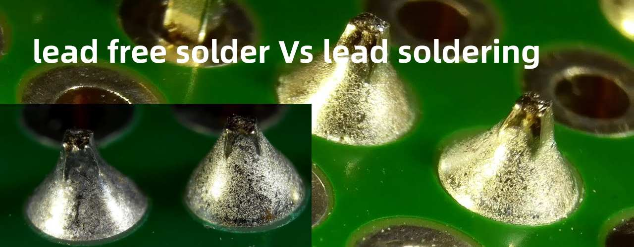
As global electronics manufacturing moves away from hazardous substances, lead free solder material has become the industry standard for PCB assembly. Driven by regulations such as RoHS and REACH, lead-free solder is now used in consumer electronics, automotive PCBs, industrial control boards, and medical devices.
However, not all lead-free solder materials are the same. Their composition, melting temperature, mechanical strength, and reliability vary significantly—making material selection critical for high-quality PCB assembly.
This guide explains what lead-free solder is, its composition, properties, types, melting temperatures, common soldering issues, and finally answers the key question: “Which lead free solder material is best for PCB assembly?”
What Is Lead Free Solder Material?
Lead free solder material is a metallic alloy used to join components to a PCB without the use of lead. Traditional solder contained 40% lead (Sn60/Pb40) or 37% lead (Sn63/Pb37). These alloys were easy to use but posed environmental and health concerns. Today, electronics manufacturers worldwide use lead-free formulations based on tin, silver, copper, bismuth, nickel, or small alloying elements.
From a customer’s perspective, lead free solder material is important because it directly affects:
Solder joint strength
Heat tolerance
Long-term reliability
Appearance of solder joints
Compatibility with high-density SMT packages
Product compliance with RoHS, REACH, and WEEE regulations
Lead-free solder also withstands higher temperatures, which is critical for modern high-density PCBs.
Is Lead-Free Solder Still Toxic?
Lead-free solder eliminates lead—a major toxic substance—but that does not mean every alloy is completely risk-free. For normal PCB manufacturing environments, lead-free solder is considered safe and non-toxic when handled properly.
From a customer standpoint:
Lead-free solder is significantly safer than leaded solder
It does not release toxic lead fumes during reflow
Flux fumes—not the solder—are usually the irritation source
Lead-free waste requires less strict disposal procedures
Most concerns come from misunderstanding. Lead-free alloys like SAC305 (Sn96.5 Ag3.0 Cu0.5) are not harmful under standard handling and reflow conditions. With adequate ventilation and proper gloves, operators face minimal exposure risks.
Lead Free Solder Material Composition
Lead-free solder material compositions vary depending on cost targets, performance needs, and thermal sensitivity of the PCB. Below is a customer-friendly comparison of common alloys:
Common lead-free soldering compositions
Alloy Type
Composition
Characteristics
Best Use
SAC305
Sn96.5 / Ag3.0 / Cu0.5
Most popular global alloy; balanced cost and performance
SMT reflow, general assembly
SAC405
Sn95.5 / Ag4.0 / Cu0.5
Higher silver for stronger joints and better wetting
Automotive, medical, mission-critical devices
SAC0307
Sn99 / Ag0.3 / Cu0.7
Cost-effective low-silver alternative
Consumer electronics, cost-controlled projects
Sn99.3Cu0.7
Tin/copper mix
Slightly higher melting point; durable in wave soldering
Wave solder baths
Sn-Bi alloys
Tin + Bismuth blends
Low melting point; ideal for heat-sensitive substrates
LED boards, flex circuits, thin PCBs
Sn-Ag alloys
Tin + Silver
Good wetting and moderate melting range
Fine-pitch soldering
Ni-doped SAC
SAC + Ni
Improved grain refinement
Automotive, aerospace
For most consumer and industrial applications, SAC305 is the ideal balance of performance and cost. Customers requiring high-temperature reliability (automotive, aerospace, telecom) may consider doped SAC alloys.
Lead Free Solder Material Properties
Lead-free solder is a low-lead soldering material based mainly on tin-based alloys such as Sn-Ag-Cu, Sn-Cu, and Sn-Bi. It is designed to replace traditional Sn-Pb solder and meet environmental regulations such as RoHS while reducing heavy-metal pollution. It’s properties can be explained from different aspects:
1. Physical & Process Characteristics
Melting Range: Wide, typically 138°C–250°C depending on alloy. SAC305 melts around 217°C. Most alloys have a narrow solid–liquid range for stable soldering.
Wetting: Good wetting behavior during reflow (30–90 seconds above liquidus) and wave soldering (≈4 seconds contact), forming reliable joints.
Conductivity: Electrical conductivity around ≥9.5×10⁶ S/m and thermal conductivity near 66 W/m·K, similar to Sn-Pb alloys.
Oxidation & Flow: Strong anti-oxidation and smooth flow with low dross generation, reducing defects such as bridging and solder spikes.
2. Mechanical Performance
Strength & Fatigue: Mechanical strength and fatigue life can be optimized through alloy design. Sn-Ag-Cu systems (e.g., 95.4Sn/3.1Ag/1.5Cu) offer strength comparable to or better than Sn-Pb.
Brittleness: Higher Ag or Cu content may reduce ductility, so alloy balance is important.
Reliability: Lead-free joints maintain stability under vibration and thermal cycling, suitable for harsh applications like automotive electronics.
3. Environmental & Cost Characteristics
Compliance: Lead content is typically below 1000 ppm, fully RoHS-compliant and safer for workers and the environment.
Cost: Generally 2–3× higher than traditional solder due to tin and silver pricing, but the impact on total product cost is usually limited.
4. Application & Compatibility
Lead-free solder is widely used in consumer electronics, automotive systems, medical devices, and new-energy applications. It works with standard fluxes and existing equipment such as 8-zone reflow ovens, though reflow profiles and process parameters may require adjustment to accommodate higher melting temperatures.
Types of Lead Free Soldering Method
Lead-free soldering involves several manufacturing methods designed around different processes, temperature profiles, and assembly requirements. When customers review PCB assembly quotes, the type of soldering used has a major impact on product durability, electrical integrity, and cost. Below are the core types of lead free soldering used in modern electronics production.
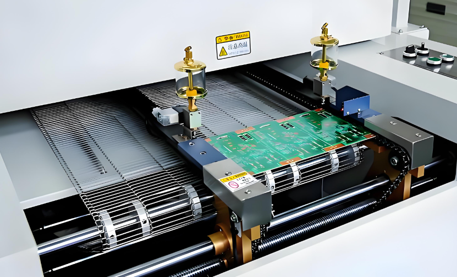
1. Lead-Free Reflow Soldering (SMT Reflow)
This is the most common method for mounting surface-mount components (SMDs). Manufacturers print lead-free solder paste onto pads, place components via pick-and-place machines, and heat the PCB in a controlled reflow oven. Reflow soldering has many advantages:
Suitable for nearly all SMT components
Works with SAC305, SAC405, SAC0307, and Sn-Bi pastes
Ensures consistent joint quality in mass production
235–250°C, depending on the alloy and PCB materials
Reflow soldering is the backbone of every modern SMT line and the main reason SAC305 is widely used.
2. Lead-Free Wave Soldering
Wave soldering is used primarily for through-hole components and mixed-technology assemblies.
During lead-free wave soldering, the PCB passes over a molten solder “wave” typically made of Sn99.3Cu0.7 or other tin-rich alloys.
Why customers care:
Ideal for high-volume assemblies with many through-hole connectors
Faster than hand soldering
Strong, uniform joints across large PCBs
But requires strict temperature control due to higher melting points
Common lead-free wave solder alloy
Sn99.3/Cu0.7, with optional micro-alloying (Ni, Ge) to reduce copper dissolution
Typical pot temperature
255–265°C, depending on alloy
3. Lead-Free Selective Soldering
Selective soldering is used when only certain through-hole components must be soldered without exposing the entire PCB to a wave. A programmable nozzle creates localized molten solder “mini waves.”
Why customers care:
Protects heat-sensitive components
Reduces overall thermal stress
Useful for complex PCBs with dense SMT areas
Generates precise and stable joints
Common alloys
Sn99.3Cu0.7
SAC variants for specialized cases
Selective soldering is popular in industrial controllers, automotive electronics, and telecom boards.
4. Lead-Free Hand Soldering
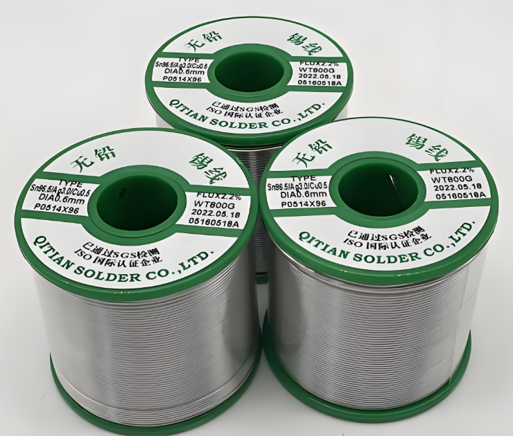
Used for repair, prototyping, or small-batch assembly. Technicians use solder wire (typically SAC305 or SAC0307) and temperature-controlled irons.
Why customers care:
Required for last-minute rework
Used in prototype and engineering samples
Easy way to repair or modify boards
Quality depends heavily on operator skill and iron temperature
Hand soldering temperature
350–380°C for SAC alloys
280–310°C for Sn-Bi low-temp solder
Here is a quick comparison between these lead-free solder material methods:
Soldering Type
Main Features
Typical Alloys
Customer Use Case
Reflow Soldering
Standard SMT process
SAC305, SAC0307
Consumer & industrial electronics
Wave Soldering
High-volume through-hole
Sn99.3Cu0.7
Power boards, large PCBs
Selective Soldering
Localized soldering
Sn-Cu, SAC
Mixed-technology PCBs
Hand Soldering
Rework / prototyping
SAC305 wire
Engineering builds, repairs
Does 60/40 Solder Contain Lead?
Yes, 60/40 solder (Sn60/Pb40) contains 40% lead, so it is not RoHS compliant and must not be used in modern commercial electronics.
Lead-free solder materials replace this alloy entirely in global manufacturing unless exemptions apply (e.g., military or aerospace exceptions).
Lead-Free Solder Melting Temperature Chart
Below is a melting temperature chart customers can use as a reference during material selection or reflow profile planning:
Lead-Free Alloy
Melting Temperature (°C)
Notes
SAC305
217–220°C
Most common for SMT
SAC405
217–225°C
Higher Ag content improves strength
SAC0307
~227°C
Budget option; slightly higher melting point
Sn99.3Cu0.7
227°C
Ideal for wave soldering
Sn-Bi
138–170°C
Best for low-temp applications
Sn63/Pb37 (leaded)
183°C
For comparison only
Customers should always verify that their components can tolerate the peak reflow temperature required by the alloy.
What Are the Main Issues With Lead-Free Soldering?
Lead-free soldering is reliable, but it requires proper process control. Common challenges include:
Higher melting point that stresses components
Slower wetting that demands optimized flux
Sometimes duller appearance of joints
Increased copper dissolution in wave soldering
Sensitivity to reflow temperature deviations
Why Is My Lead-Free Solder Not Melting?
Typical causes include:
Iron or reflow temperature not high enough.
Insufficient heat transfer due to oxidation or contamination.
Using a low-power soldering iron unable to maintain temperature.
Weak flux activity preventing proper heat flow.
Applying the solder to a large thermal pad without preheating.
Lead-free solder requires around 30–40°C higher heat than leaded solder.
Which Lead Free Solder Material Is Best for PCB Assembly?
For most customers, SAC305 (Sn96.5/Ag3.0/Cu0.5) is the best lead-free solder material for PCB assembly.
Why SAC305 Is Ideal for Most Applications?
Widely used across global SMT factories
Excellent wetting on FR4, HDI, flexible, and ceramic substrates
Strong mechanical performance
Good thermal cycling reliability
Low voiding rate with proper reflow control
Compatible with nearly all flux chemistries
Proven in millions of consumer and industrial electronics
When Other Alloys Might Be Better?
SAC0307 – When cost is the priority
Sn-Bi – For low-temperature PCBs and LED products
SAC405 – For high-reliability automotive or medical electronics
Sn99.3Cu0.7 – For wave soldering to reduce cost
Customer Recommendation
If you are unsure which alloy to choose, start with SAC305 for standard SMT reflow because it aligns with:
Reliability expectations
Cost targets
Compatibility with modern assembly lines
Strong field performance
FAQs
1. What is the most common lead-free solder in SMT assembly?
SAC305 is the industry standard for most SMT production lines.
2. Is lead-free solder as strong as leaded solder?
Yes. Lead-free joints are typically stronger in mechanical strength and thermal fatigue resistance.
3. Why is lead-free solder harder to work with manually?
It melts at a higher temperature and wets more slowly, requiring better temperature control.
4. What flux should be used with lead-free solder?
Most solder pastes use no-clean or water-soluble fluxes optimized for SAC alloys.
5. Can lead-free solder be used with ENIG finish?
Yes, ENIG is one of the best surface finishes for consistent wetting.
Choosing the right manufacturing model is one of the most important strategic decisions for electronics companies. In the PCB and PCBA sector, product lifecycles are shorter, technical requirements are higher, and global competition is stronger than ever. In this environment, two models, OEM and ODM, shape how your boards move from idea to mass production.
This guide explains both models in clear terms, compares them using real PCB scenarios, and provides a practical decision framework that engineers, buyers, and founders can use when planning their next PCB or PCBA project.
What Is OEM Manufacturing in the PCB Industry?
OEM manufacturing refers to a model where the customer owns the product design, controls the technical specifications, and provides the documentation needed for production. In the PCB field, an OEM project usually includes:
Complete Gerber files and drill files
Stack-up information and layer count definition
Bill of materials (BOM) with approved vendor list
Assembly drawings and mechanical constraints
Testing procedures and acceptance criteria
Quality and reliability requirements
Under the OEM model, the PCB manufacturer acts as a specialist executor. The factory fabricates boards, assembles components, and runs tests in strict alignment with the customer’s design and documentation.
The engineering ownership remains on the customer side, while the manufacturer delivers robust production, process control, and supply chain support.
In the PCB industry, OEM manufacturing is common in fields where design control and traceability matter:
Medical instrumentation and life-support electronics
Automotive electronics and ADAS-related boards
Aerospace and defense control modules
High-frequency RF and microwave PCBs
Industrial automation controllers
Robotics and motion control systems
These applications often involve tight regulations, proprietary algorithms, and long-term maintenance. Companies choose the OEM path because it allows them to keep full control of their PCB design while relying on an experienced manufacturing partner for fabrication, assembly, and testing.
What Is ODM Manufacturing in the PCB Industry?
ODM manufacturing goes beyond production and includes design and development. Instead of providing a finished design, the customer shares functional requirements, performance targets, and budget expectations. The ODM manufacturer then handles engineering and turns the requirements into a manufacturable PCB or PCBA solution.
Typical ODM services in the PCB domain include:
Circuit concept and schematic design
PCB layout and stack-up planning
Component selection and alternative sourcing
Design for manufacturability (DFM) and design for assembly (DFA)
Prototype build and design iterations
Compliance support and basic certification guidance
Full-scale production and functional testing
Many growing electronics brands, start-ups, and non-technical founders choose ODM when they need a finished PCB solution but do not have sufficient internal engineering resources. The manufacturer becomes both a design partner and a production partner.
In the PCB and PCBA world, ODM is frequently used for:
IoT sensor nodes and gateways
Smart home and building automation devices
Wearable electronics and fitness trackers
LED lighting drivers and control boards
Consumer electronics modules and controller boards
Low-power wireless communication boards
These market segments evolve quickly and demand frequent updates. A capable ODM PCB partner can speed up development and help clients get new boards into the market much faster.
OEM vs ODM: Core Differences for PCB and PCBA Projects
Both OEM and ODM are valuable, but they solve different problems. Understanding how they differ helps you select the model that fits your product, budget, and timeline.
Area
OEM
ODM
Design Ownership
Customer owns design, files, and IP
Manufacturer often owns design unless transferred by contract
Shorter due to in-house design resources and templates
Engineering Support
Focused on DFM, DFA, and production advice
Full design plus optimization support
MOQ Flexibility
Often higher for mature products
Can be lower for pilot and first launches
Customization Level
Unlimited customization within process capability
Often based on existing platforms or reference designs
IP Protection
Very strong, assuming secure data handling
Contract-dependent; must be clearly defined
Risk Profile
Lower in production, higher in internal design quality
Lower design risk, but higher IP and dependency risk
Engineers often pick the OEM route when they need tight control over design, especially for high-end or regulated PCBs. Teams that prioritize speed, flexibility, and reduced internal workload tend to lean toward ODM.
When Should a PCB Company Choose OEM?
The OEM manufacturing model is ideal when technical control, long-term stability, and full customization are your highest priorities.
You should prefer OEM when:
You already have a PCB design or a strong internal R&D and layout team.
Your product must comply with strict standards such as ISO 13485, IATF 16949, or specific medical or automotive norms.
You handle sensitive RF front-ends, custom impedance structures, or advanced HDI designs.
You plan to maintain and update your product over many years.
You want full freedom to switch manufacturers while keeping the same design.
In these situations, working with an experienced OEM PCB partner gives you manufacturing stability while you retain all core design decisions. This model suits companies that treat their PCB design as a central asset in their business.
When Is ODM the Better Option for PCB Projects?
The ODM model is a better fit when you care most about speed, simplified development, and reduced engineering overhead.
Consider ODM when:
You have a clear product idea but no detailed PCB design.
Your team lacks time or skills to manage schematics and layout.
You want to test a new market quickly and validate demand with a working prototype.
Your project falls into categories with fast refresh cycles, such as IoT or consumer electronics.
You prefer a one-stop solution from concept through production and assembly.
An experienced ODM PCB partner can turn functional requirements into a board design, prototype it, optimize for manufacturing, and ramp into production. This is especially valuable for start-ups and smaller brands that want to focus more on marketing and sales while outsourcing technical development.
OEM and ODM Pricing Models and Cost Drivers in PCB Manufacturing
Both OEM and ODM projects are influenced by similar manufacturing cost factors, but their structures differ at the development stage.
Key Cost Drivers for OEM PCB Projects
Base material type (standard FR4, high-Tg, Rogers, ceramic, metal-core)
Layer count, board thickness, and stack-up complexity
Trace width and spacing, especially in HDI designs
Via types (through-hole, buried, blind, microvias)
In OEM projects, design work is already complete, so development cost is mainly related to DFM review and minor adjustments. The main financial focus is on fabrication, assembly, materials, and testing.
Key Cost Drivers for ODM PCB Projects
Concept definition and hardware architecture
Schematic capture and simulation if required
PCB layout and optimization cycles
Prototype iterations and validation builds
Component selection, sourcing, and second-source planning
Compliance support and pre-certification testing where needed
In ODM projects, you pay for additional engineering work in exchange for a much lighter internal workload and a faster path to a finished board. The overall cost can be very competitive when you consider the time saved and the opportunity to reach the market earlier.
How to Protect Your IP with OEM and ODM PCB Partners
Intellectual property protection is one of the most sensitive topics when companies decide between OEM and ODM. While no model is completely risk-free, there are practical steps that significantly reduce exposure.
Formal NDAs and Manufacturing Agreements: Clearly define confidentiality around schematics, Gerber files, BOM, firmware, and test tools.
Contractual IP Ownership: In ODM projects, specify whether IP will be transferred, shared, or licensed.
Controlled File Sharing: Limit sensitive design information to dedicated engineering contacts.
Firmware Protection: Use secure bootloaders, encryption, and lock bits for microcontrollers when needed.
Selection of Certified Partners: Choose factories with ISO and industry-specific certifications that follow disciplined processes.
With a solid legal framework and careful partner selection, both OEM and ODM collaborations can support long-term, secure PCB programs.
Quality Control Strategies for OEM and ODM PCB Production
Reliable PCB performance comes from consistent process control, not only from design quality. A professional PCB supplier, whether working under an OEM or ODM model, should implement a systematic quality strategy.
Incoming quality control (IQC) for copper clad laminates, solder paste, and components
In-process checks (IPQC) at critical stages such as etching, drilling, plating, and soldering
Automated optical inspection (AOI) for bare boards and assembled boards
Solder paste inspection (SPI) for SMT process control
X-ray inspection for BGA, QFN, and hidden joints
Electrical tests (flying probe or ICT) for open and short detection
Functional tests and burn-in for mission-critical products
In ODM projects, additional validation is often required at the prototype stage, because the design is fresh. In OEM projects, focus is more on maintaining stable yields and repeatability once the design is frozen.
How to Evaluate and Select a Reliable OEM or ODM PCB Supplier
Selecting your manufacturing partner is a decision that affects product quality, lead time, cost, and even brand reputation. Whether you prefer OEM or ODM, certain evaluation points remain essential.
Engineering Capability: Can the supplier handle HDI, RF, flex, rigid-flex, ceramic, or heavy copper boards?
DFM and DFA Support: Do they proactively optimize your design for yield and manufacturability?
In-house SMT and Assembly: One-stop fabrication and PCBA in locations such as China and Vietnam improves coordination.
Certifications: Look for ISO 9001, ISO 13485, IATF 16949, and UL where relevant.
Equipment Level: Advanced drilling, imaging, solder mask, SPI, AOI, and reflow lines reflect process strength.
Prototype and Low-volume Capability: This is vital for early-stage ODM projects and design validation.
Communication and Project Management: Clear, responsive communication reduces delays and misunderstandings.
A strong PCB partner is more than a factory. It should be a technical advisor that helps you reduce risk and increase reliability.
OEM and ODM Examples Across PCB-Intensive Industries
Both OEM and ODM models are widely used across industries that rely heavily on PCBs and assembled boards.
Typical OEM PCB Applications
Medical diagnostics and laboratory equipment PCBs
Industrial motion control and PLC boards
Automotive control modules and sensor interfaces
High-speed communication backbone boards
Ceramic-based power modules for power electronics
Typical ODM PCB Applications
Smart home controllers and gateways
IoT sensor nodes and tracking devices
Wearable health monitors
LED lighting drivers and control PCBs
Compact consumer product controller boards
These examples show that both models are valid tools. The choice is not about which one is absolutely better, but about which one matches your product and business goals.
FAQs: OEM and ODM for PCB and PCBA
Below are some of the most common questions engineers, buyers, and founders ask when comparing OEM and ODM in the PCB domain.
Q1. Is OEM always more expensive than ODM?
Not always. OEM projects can be cost-effective when you already have a mature design and stable volume. ODM includes engineering fees, but it saves internal R&D cost and time. The better option depends on how much design work you can handle in-house.
Q2. Do I keep my IP if I work with an ODM supplier?
IP ownership in ODM projects depends on the contract. Some suppliers transfer full design ownership to you, while others retain partial rights. Make sure ownership, licensing, and future use of the design are clearly described in your agreement.
Q3. What is the typical MOQ difference between OEM and ODM?
OEM projects often have higher MOQs because they support stable, long-term products. ODM suppliers sometimes offer lower MOQs for pilot runs or market testing, especially in consumer and IoT sectors.
Q4. Can I start with an ODM design and later move to an OEM model?
Yes. Many companies use ODM to launch fast, then move to an OEM model with a custom design once the market is proven. Carefully plan IP and file access from the start to keep this option open.
Q5. Which model is better for highly specialized or high-reliability PCBs?
For complex HDI, RF, high-speed, or safety-critical boards, OEM is usually the stronger choice. You maintain full design control and can work with a manufacturer that focuses on process excellence and reliability.
Q6. Which model helps us launch faster?
ODM typically shortens launch time because design, layout, and prototyping are handled by the manufacturer. If speed and reduced internal workload are top priorities, this model offers a practical shortcut.
How to Decide Between OEM and ODM for Your Next PCB Project?
Deciding between OEM and ODM is easier when you look at your situation through three lenses: technical control, available resources, and time to market.
Choose OEM if you:
Have or plan to build internal PCB design expertise.
Need strict IP control for competitive or regulated products.
Expect long product lifecycles and multiple future revisions.
Work in medical, automotive, aerospace, or other high-reliability areas.
Choose ODM if you:
Want to turn a product concept into a ready PCB quickly.
Prefer to outsource heavy engineering work.
Operate in fast-changing consumer or IoT markets.
Need a one-stop partner for design, fabrication, assembly, and testing.
In practice, many companies use both models at different stages. They may rely on ODM partners for early concepts and market tests, then shift to an OEM model once volumes grow and the product stabilizes. By matching the model to each development phase, you can control cost, manage risk, and keep your roadmap flexible.
This website uses cookies to enhance your experience, remember your preferences, and help us understand how visitors use our site. You can accept all cookies, reject non-essential cookies, or manage your settings.
This website uses cookies to improve your experience while you navigate through the website. Out of these cookies, the cookies that are categorized as necessary are stored on your browser as they are essential for the working of basic functionalities of the website. We also use third-party cookies that help us analyze and understand how you use this website. These cookies will be stored in your browser only with your consent. You also have the option to opt-out of these cookies. But opting out of some of these cookies may have an effect on your browsing experience.
Necessary cookies are absolutely essential for the website to function properly. These cookies ensure basic functionalities and security features of the website, anonymously.
Cookie
Duration
Description
cookielawinfo-checkbox-analytics
11 months
This cookie is set by GDPR Cookie Consent plugin. The cookie is used to store the user consent for the cookies in the category "Analytics".
cookielawinfo-checkbox-functional
11 months
The cookie is set by GDPR cookie consent to record the user consent for the cookies in the category "Functional".
cookielawinfo-checkbox-necessary
11 months
This cookie is set by GDPR Cookie Consent plugin. The cookies is used to store the user consent for the cookies in the category "Necessary".
cookielawinfo-checkbox-others
11 months
This cookie is set by GDPR Cookie Consent plugin. The cookie is used to store the user consent for the cookies in the category "Other.
cookielawinfo-checkbox-performance
11 months
This cookie is set by GDPR Cookie Consent plugin. The cookie is used to store the user consent for the cookies in the category "Performance".
viewed_cookie_policy
11 months
The cookie is set by the GDPR Cookie Consent plugin and is used to store whether or not user has consented to the use of cookies. It does not store any personal data.
Functional cookies help to perform certain functionalities like sharing the content of the website on social media platforms, collect feedbacks, and other third-party features.
Performance cookies are used to understand and analyze the key performance indexes of the website which helps in delivering a better user experience for the visitors.
Analytical cookies are used to understand how visitors interact with the website. These cookies help provide information on metrics the number of visitors, bounce rate, traffic source, etc.
Advertisement cookies are used to provide visitors with relevant ads and marketing campaigns. These cookies track visitors across websites and collect information to provide customized ads.