Electronics PCB manufacturing is the lifeblood of modern technology. This guide explores its types, quality control, and how to choose a top partner like EBest Circuit (Best Technology) for reliable, high-performance circuit boards.
What are the typical pain points companies face when sourcing PCBs?
- Unreliable Quality: Boards failing after a short period of use.
- Inconsistent Delivery Times: Unpredictable production schedules.
- Poor Communication: Slow responses and lack of technical support.
- Hidden Costs: Surprising charges that appear after ordering.
- Limited Technical Capability: Manufacturers unable to handle complex designs.
Fortunately, these problems are entirely avoidable. The solutions provided by EBest Circuit (Best Technology) directly address these concerns:
- Rigorous Quality Control: We implement a multi-stage inspection system. Every electronic PCB board manufacturer process is monitored to ensure zero defects.
- Structured Production Planning: Our advanced planning ensures on-time delivery. We keep your projects moving smoothly.
- Dedicated Engineering Support: You get a single point of contact. Our team provides proactive updates and expert advice.
- Transparent Quoting: We provide clear, upfront pricing. There are no surprises, helping you manage your electronics PCB manufacturing cost effectively.
- Advanced Technical Expertise: Our factory is equipped for sophisticated projects. We specialize in complex multilayer PCB manufacturing process.
For over 19 years, EBest Circuit (Best Technology) has been a trusted PCB and flexible circuit solutions provider, turning complex requirements into high quality electronic boards. Our expertise is proven by advanced capabilities in manufacturing high-layer counts up to 32 layers, handling extreme copper weights from 1oz to 20oz, and achieving precise features like 3/3 mil line spacing and 0.1mm micro-vias. For a expert consultation, reach us at sales@bestpcbs.com.
Why Electronics PCB Manufacturing Is Critical for Modern Devices?
At the heart of every modern electronic device lies its printed circuit board (PCB). More than just a platform for components, the PCB is the central nervous system of your product, determining its performance, reliability, and longevity. The choice of your PCB manufacturer is therefore not a simple procurement step; it is a strategic engineering decision.
From Design to Better Quality Electronic PCBs:
A design file is a perfect, theoretical model. Transforming it into a high-functioning physical board is where professional manufacturing makes the critical difference. This process hinges on several key capabilities:
- Signal Integrity & Material Science: High-speed digital and high-frequency RF designs (like those in 5G and IoT devices) demand precise control over electrical signals. Professional manufacturers achieve this through expertise in selecting specialized materials (like Rogers or Isola laminates) and controlling impedance with tolerances as tight as ±10%. Amateur fabrication can lead to signal loss, crosstalk, and data corruption.
- Power Integrity & Thermal Management: Modern processors and ASICs require stable, clean power. This is ensured through sophisticated multilayer stack-ups with dedicated power and ground planes. Furthermore, effective thermal management via thermal vias and appropriate copper weights (e.g., 2oz for power circuits) prevents overheating, ensuring device stability and a longer lifespan.
- Miniaturization and Reliability (HDI): As devices shrink and become more powerful, High-Density Interconnect (HDI) technology is essential. This involves advanced processes like laser-drilled micro-vias (as small as 0.1mm), stacked vias, and fine-line etching (3/3 mil line/space). These techniques allow for more functionality in a smaller footprint, which is critical for wearables, medical implants, and advanced consumer electronics.
In non-critical applications, a PCB failure might mean an inconvenience. However, in several advanced industries, the stakes are significantly higher:
- Automotive: PCBs must withstand extreme temperatures, constant vibration, and humidity. They are the backbone of safety systems like ABS and airbag control units. Failure is not an option.
- Medical: Devices for diagnostics and patient monitoring require absolute reliability. They often need to be biocompatible and manufactured in certified cleanrooms to ISO 13485 standards.
- Aerospace & Defense: Boards must perform flawlessly under intense stress and in harsh environments, adhering to stringent standards like IPC-A-610 Class 3.
Choosing EBest Circuit (Best Technology) means partnering with experts who translate your complex designs into reliable, high-performance hardware. We bring over 19 years of focused expertise in advanced PCB and flexible circuit manufacturing. Ready to discuss how our manufacturing capabilities can bring robustness and reliability to your next project? Contact our engineering team at sales@bestpcbs.com for a consultation.
What are the Types of Electronics PCB Manufacturing?
Selecting the appropriate PCB type is a foundational engineering decision that directly impacts the performance, reliability, and cost of an electronic device. Moving beyond basic definitions, a deeper understanding of the classifications and their manufacturing implications is crucial. Here is a detailed breakdown based on industry standards and advanced fabrication capabilities.
1. Classification by Layer Count and Structure
This is the primary way to categorize PCBs, reflecting their complexity.
- Single-Sided PCBs: Featuring a single conductive copper layer on one side of a substrate, these are the most straightforward to manufacture. They are cost-effective and ideal for simple, low-density circuits but offer limited functionality for modern devices.
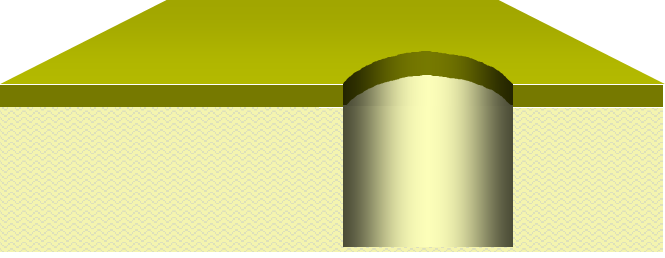
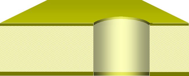
- Double-Sided PCBs: These boards have conductive layers on both the top and bottom surfaces, connected by Plated Through-Holes (PTH). This doubles the available area for components and routing, making them a versatile and common choice for a wide range of applications, from industrial controls to consumer electronics.
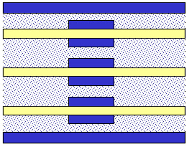
- Multilayer PCBs: Defined as having three or more conductive layers, these boards are essential for complex, high-speed electronics. Layers are laminated together with insulating prepreg (PP) under high temperature and pressure.
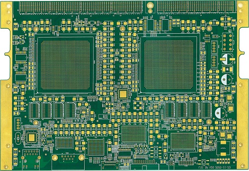
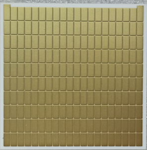
- Capability Spotlight: Modern manufacturing, as detailed in your materials, can produce boards with up to 32 layers. High-TG (Glass Transition Temperature) materials, such as KB6167 or IT180, are often mandatory for boards exceeding 8 layers to ensure stability during the lamination process and under operational heat. The picture below is an 8-layer board for your reference.
2. Classification by Physical Properties: Rigidity and Flexibility
The base material defines the physical form of the board, enabling innovative product designs.
- Rigid PCBs: The most common type, built on inflexible substrates like FR-4. They provide excellent mechanical support and are used in the vast majority of electronic equipment where the board does not need to move or bend.
- Flexible PCBs (FPC): Manufactured on flexible plastic substrates like polyimide. Their key advantages include high flexibility, light weight, and excellent resistance to heat and vibration. They are perfect for dynamic applications or tight spaces, such as in cameras, wearable devices, and within automotive assemblies.
- Rigid-Flex PCBs: This advanced hybrid integrates rigid boards for component support with flexible interconnects into a single structure. This combination simplifies the overall assembly, enhances reliability by eliminating the need for connectors between rigid boards, and allows for more compact, three-dimensional packaging.
3. Classification by Surface Finish
The surface finish is a critical quality factor, protecting the copper from oxidation and ensuring solderability. Your document lists an extensive portfolio, including:
- HASL (Hot Air Solder Leveling): A common, cost-effective finish for general purposes.
- ENIG (Electroless Nickel Immersion Gold): Provides a flat surface, excellent for fine-pitch components and offering good oxidation resistance.
- Immersion Silver/Tin: Offers good performance for a range of applications.
- ENEPIG (Electroless Nickel Electroless Palladium Immersion Gold): A premium finish with superior wire-bonding capability and resistance to corrosion.
- Gold Finger Plating: Used for edge connectors, requiring a hard, durable gold plating. Combinations like HASL + Gold Finger or ENIG + OSP are also standard offerings to meet specific zone-specific requirements on a single board.
4. Classification by Specialized Material Properties
For high-performance applications, the base laminate material is specially engineered.
- High-Frequency/High-Speed PCBs: These use specialized laminates (e.g., Rogers, Taconic) with controlled dielectric constants (Dk) and dissipation factors (Df) to maintain signal integrity at high frequencies, which is critical for 5G, radar, and satellite communications.
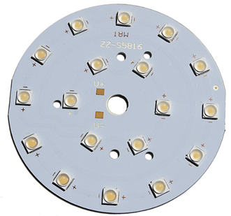
- Metal-Clad PCBs (MCPCB): Designed for superior thermal management. They feature a metal base (typically aluminum or copper) that draws heat away from critical components, making them ideal for high-power LED lighting, power supplies, and automotive systems.
- Ceramic PCBs: Offer exceptional thermal conductivity, electrical insulation, and stability in high-temperature environments, used in high-power modules and aerospace applications.
5. Classification by Via Technology
The method of creating connections between layers is a key differentiator in advanced PCB manufacturing.
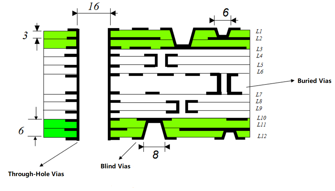
- Through-Hole Vias: Standard vias drilled through the entire board.
- Blind Vias: Connect an outer layer to one or more inner layers, but do not go through the entire board.
- Buried Vias: Connect internal layers without reaching the outer surfaces.
- Microvias: These are small vias (typically with a diameter of 0.1mm or less) created by laser drilling. They are a cornerstone of HDI (High-Density Interconnect) technology, allowing for much higher wiring density and are essential for compact devices like smartphones.
In conclusion, the choice of PCB type is a strategic decision intertwined with your product’s electrical, thermal, and mechanical requirements. Partnering with a manufacturer like BEST Technology, which possesses the expertise across this full spectrum—from standard FR-4 to complex HDI and rigid-flex boards—ensures that your design is built on a foundation of reliability and performance.
How EBest Circuit (Best Technology) Excels in Electronics PCB Manufacturing for Global Clients?
In a competitive global market, excellence is not an accident. It is the result of a systematic commitment to quality, service, and innovation. EBest Circuit (Best Technology) stands out by focusing on what truly matters to our clients.
- First, our quality control is uncompromising. We employ Statistical Process Control (SPC) at key stages. Our MES (Manufacturing Execution System) provides full traceability. You can trace every board back to its production batch. This is critical for quality assurance and continuous improvement.
- Second, we provide unparalleled engineering support. Our team doesn’t just build your design; we partner with you to optimize it. We offer Design for Manufacturability (DFM) feedback. This helps prevent potential issues before production begins. It saves you time and reduces the cost of PCB manufacturing.
- Third, we understand the importance of cost-efficiency. By optimizing our processes and maintaining strong supplier relationships, we offer highly competitive pricing without sacrificing quality. We give you clear insights into your electronics PCB manufacturing cost.
- Finally, our customer service is proactive and responsive. We assign a dedicated project manager to your account. You will receive regular updates, ensuring you are always informed. This level of service builds trust and long-term partnerships.
Technical Capability for Electronic PCB Manufacturer
As a leading specialist in PCB fabrication, EBest Circuit (Best Technology) possesses extensive manufacturing capabilities to meet the demanding requirements of various industries, from consumer electronics to high-reliability automotive and telecommunications applications. Our technical prowess is detailed below, demonstrating our commitment to precision, quality, and innovation.
1. Materials
We support a comprehensive range of substrate materials to cater to diverse electrical and thermal performance needs:
- FR-4 Series: Standard TG (130-140°C), Mid TG (150°C), and High TG (170-180°C). We utilize premium brands like KB, Shengyi, and ITEQ, including halogen-free options.
- High CTI Materials: Such as Shengyi S1600L for enhanced comparative tracking index.
- High-Speed/Low-Loss Materials: Capable of processing mid-loss (e.g., IT-968, TU-883), low-loss (e.g., IT-958, TU-872SLK), and ultra-low-loss (e.g., IT-933, TU-993) laminates, including Isola products.
- High-Frequency Materials: Expertise in ceramic-filled (e.g., Rogers 4350B, 4003) and PTFE-based (e.g., Rogers, Taconic, Arlon) materials for RF and microwave applications.
2. Layer Count
We manufacture printed circuit boards with a wide range of complexity:
- Standard Capability: 1 to 50 layers.
- Advanced Capability: Up to 100 layers (subject to technical review for boards exceeding 50 layers).
3. Board Thickness
We offer flexibility in board thickness with tight control over tolerances:
- Standard Range: 0.4mm to 6.0mm.
- Advanced Range: 0.15mm to 10.0mm.
- Thickness Tolerance: ±0.1mm for boards ≤1.0mm; ±10% for boards >1.0mm. Tighter special tolerances are available upon request.
4. Surface Finish
A variety of surface finishes are available to ensure solderability and end-use performance:
- Lead-Free Finishes: HASL, ENIG (Immersion Gold), Immersion Tin, Immersion Silver, OSP, Hard/Soft Gold Plating (with/without Nickel), ENIG+OSP, ENEPIG, and Plated Gold Fingers.
- Lead-Based Finishes: Leaded HASL.
5. Copper Thickness
Our processes support significant copper weights for power-intensive applications:
- FR-4 PCBs:
- Inner Layers: 0.5 oz to 6 oz (Standard); up to 20 oz (Advanced, subject to review for ≥12 oz).
- Outer Layers: 0.5 oz to 10 oz (Standard); up to 28 oz (Advanced).
- High-Frequency/Speed PCBs:
- Inner Layers: 0.5 oz to 1 oz (Standard); up to 2 oz (Advanced).
- Outer Layers: 0.5 oz to 2 oz (Standard); up to 3 oz (Advanced).
6. Board Dimensions
We accommodate a wide spectrum of board sizes:
- Minimum Finished Size: 10mm x 10mm (Standard); 3mm x 3mm (Advanced).
- Maximum Finished Size:
- ≤2 layers: 580mm x 890mm.
- ≥3 layers: 580mm x 762mm.
- Advanced: 580mm x 1220mm (with constraints).
7. Drilling
Precision drilling capabilities are central to our high-density interconnect (HDI) and standard PCB production:
- Laser Drilling: Minimum hole diameter of 0.10mm (Standard) / 0.070mm (Advanced), with a maximum aspect ratio of 1:1.
- Mechanical Drilling: Finished hole diameter range of 0.15mm to 6.5mm.
- Aspect Ratio: Up to 12:1 for through-holes (Standard) and up to 25:1 (Advanced).
- Back Drilling: Available for stub removal, with diameters from 0.4mm to 6.5mm.
- Tolerances: Hole position accuracy ±0.076mm (Standard) / ±0.05mm (Advanced).
8. Spacing (Clearances)
We maintain strict control over electrical clearances for reliability:
- Laser Drilling to Conductor: 0.20mm (Standard) / 0.15mm (Advanced).
- Mechanical Drilling to Conductor: Ranges from 0.18mm to 0.25mm depending on layer count and structure.
- Minimum Solder Mask Dam (Solder Mask Bridge): 0.10mm for 1 oz copper.
9. Line Width/Space
Our imaging and etching processes achieve fine features for high-density designs:
- Inner Layer (Standard):
- 1/2 oz Cu: ≥3/3 mil (75/75 µm).
- 1/1 oz Cu: ≥4/4.5 mil (100/112.5 µm).
- 2/2 oz Cu: ≥5/7 mil (125/175 µm).
- Outer Layer (Standard):
- 1/1 oz Cu: ≥3.5/4 mil (87.5/100 µm).
- 2/2 oz Cu: ≥5/7 mil (125/175 µm).
- Tolerances: ±1mil for line widths ≤5mil; ±20% for widths >5mil (Standard).
- Minimum BGA Pad Diameter: 10mil (Standard) / 8mil (Advanced).
10. Solder Mask & Legend
We provide high-quality soldermask application and legend printing in various colors:
- Solder Mask Colors: Green, Black, Blue, Red, White, Yellow, Purple, Matte Green, Matte Black, Matte Blue.
- Legend Colors: White, Black.
- Solder Mask Registration: ±0.076mm (Standard) / ±0.05mm (Advanced).
- Minimum Solder Mask Web (Bridge): 0.1mm for 1oz copper with standard green LPI.
11. Via Plugging (Resin/Copper Filling)
Capable of filling vias to create a planar surface and prevent solder wicking:
- Finished Hole Diameter: 0.1mm to 0.8mm.
- Maximum Aspect Ratio (Board Thickness/Hole Diameter): 10:1 (Standard) / 25:1 (Advanced).
12. Outline & Routing
Precision routing and scoring services ensure accurate board dimensions and clean break-outs:
- Outline Tolerance: ±0.13mm (Standard) / ±0.10mm (CNC) or ±0.05mm (Laser Cutting, for boards ≤1.0mm) (Advanced).
- V-Scoring: Available at 20°, 30°, 45°, and 60° angles. Suitable for board thicknesses from 0.5mm to 4.0mm.
13. Surface Coating Thickness
We ensure consistent and compliant thickness for all surface finishes:
- ENIG (Immersion Gold): Au: 0.025-0.125µm; Ni: 3-8µm.
- HASL (Lead-Free): 2-40µm.
- Immersion Silver: 0.2-0.4µm.
- OSP: 0.1-0.3µm.
- Plated Gold Finger: 0.1-1.27µm.
14. Other Key Capabilities
- Impedance Control: Tight tolerance of ±10% (≥50Ω) (Standard) / ±6% (Advanced).
- Bow and Twist: ≤0.75% (Standard) / ≤0.5% (Advanced).
- Layer-to-Layer Registration: ≤0.15mm (Standard) / ≤0.13mm (Advanced).
15. Metal Core PCBs (MCPCB)
We specialize in manufacturing Aluminum and Copper-based PCBs for superior thermal management:
- Layer Count: 1 to 6 layers (>6 layers subject to review).
- Board Thickness: 0.5mm to 5.0mm.
- Copper Thickness: 0.5 oz to 3 oz (>3 oz subject to review).
- Thermal Conductivity: Supports materials with conductivity from 0.3 W/m·K to 6.0 W/m·K (Standard), and up to 12 W/m·K (Advanced).
- Metal Base Thickness: 0.5mm to 5.0mm.
This overview underscores EBest Circuit (Best Technology)’s capacity to deliver high-quality, reliable PCBs tailored to your specific design requirements. Our engineering team is available for consultation to ensure your project’s success.
Multilayer PCB Manufacturing Process – EBest Circuit (Best Technology)
Transforming a complex circuit design into a reliable, high-performance multilayer Printed Circuit Board (PCB) is a feat of precision engineering. At EBest Circuit (Best Technology), our process for manufacturing boards from 4 to over 24 layers is built upon rigorous control and advanced capabilities at every stage. The following outline details the critical steps that ensure the integrity of your product’s foundation.
Phase 1: Inner Layer Fabrication – Creating the Internal Circuitry
This phase focuses on manufacturing the individual conductive layers that will be laminated inside the board.
- Step 1: Panel Preparation (Board Cut)
- Large sheets of copper-clad laminate (CCL) are precision-cut into smaller, standardized production panels. The primary goal is to maximize material utilization while meeting the design’s dimensional requirements.
- Step 2: Inner Layer Imaging (Pattern Transfer)
- Cleaning and Dry Film Lamination: The panel surface is thoroughly cleaned and then coated with a light-sensitive dry film.
- Exposure: Ultraviolet light is projected through a photographic film (phototool) containing the circuit pattern onto the dry film, hardening the exposed areas.
- Development: The unhardened dry film is chemically dissolved, revealing the copper that is not part of the desired circuit.
- Etching and Stripping: The exposed copper is etched away. The remaining hardened dry film is then stripped off, leaving behind the precise copper circuitry.
- Step 3: Automated Optical Inspection (AOI) & Oxide Treatment
- Each inner layer is automatically scanned to detect any defects, such as shorts or opens. The layer then undergoes an oxide treatment (browning) to improve adhesion during the lamination process.
Phase 2: Layer Stack-Up and Lamination – Building the Multilayer Structure
The individual layers are assembled and bonded into a single, solid board.
- Step 4: Lay-Up
- The inner layers, sheets of insulating prepreg (B-stage epoxy resin), and outer layer copper foil are meticulously aligned and stacked in a specific sequence.
- Step 5: Lamination Press
- The stack is subjected to high temperature (approximately 200°C) and pressure in a hydraulic press. This causes the prepreg resin to melt, flow, and permanently cure, bonding the layers together. A controlled cooling cycle under pressure is critical to prevent warping.
Phase 3: Drilling and Plating – Establishing Interlayer Connections
Holes are drilled and metallized to create electrical pathways between the different layers of the board.
- Step 6: Precision Drilling
- Using Computer-Numerical Control (CNC) machines, holes for vias and component leads are drilled. We support a wide range of drill bit sizes, from 0.15mm for microvias to 6.5mm for larger tooling holes. For high-density designs, we utilize advanced laser drilling.
- Step 7: Hole Metallization (Desmear & Electroless Copper Deposition)
- This is a critical chemical process. It begins with desmear to remove epoxy residue from the drilled hole walls. The panel then undergoes a series of baths that deposit a thin, conductive layer of copper (typically 1-3µm) onto the entire panel surface, including the hole walls, making them electrically conductive.
Phase 4: Outer Layer Formation – Completing the Circuit
The outer layers are patterned and plated to finalize the board’s circuitry.
- Step 8: Panel Electrolytic Plating
- The panel is plated with copper to increase the thickness of the conductive layer on the surface and within the holes, ensuring robust electrical connections.
- Step 9: Outer Layer Imaging & Pattern Plating
- A dry film is applied, exposed (often using high-precision Laser Direct Imaging – LDI), and developed to define the outer layer circuit pattern.
- The panel is plated again with copper to build up the traces and pads, followed by a layer of tin, which acts as an etch resist.
- Step 10: Etching (Strip-Etch-Strip)
- The dry film is stripped away. The underlying copper is then etched, but the tin-plated circuits are protected. Finally, the tin is stripped, revealing the final, precise outer layer circuits.
Phase 5: Solder Mask and Surface Finish – Application and Protection
The board is prepared for component assembly.
- Step 11: Solder Mask Application
- A liquid photoimageable solder mask ink (typically green, but other colors are available) is applied to the panel. It is then exposed and developed to open windows over the solderable pads, protecting the copper circuitry from oxidation and preventing solder bridges.
- Step 12: Surface Finish Application
- A final coating is applied to the exposed copper pads to ensure reliable solderability. We offer a wide range of finishes, including HASL (Lead-free), ENIG (Electroless Nickel Immersion Gold), Immersion Silver, Immersion Tin, and ENEPIG (Electroless Nickel Electroless Palladium Immersion Gold).
- Step 13: Legend Printing (Silkscreen)
- Component designators, logos, and other markings are printed onto the board surface using epoxy ink, typically in white.
Phase 6: Final Fabrication, Testing, and Inspection
The individual boards are separated and subjected to final quality assurance.
- Step 14: Profiling (Routing)
- The individual PCBs are routed out of the production panel using CNC milling machines, V-scoring, or laser cutting.
- Step 15: Electrical Testing
- Every board undergoes 100% electrical testing. Flying Probe testers are used for prototypes and small batches, while custom test fixtures are employed for high-volume production to verify electrical continuity and isolation.
- Step 16: Final Quality Control (FQC) & Packaging
- A comprehensive visual and dimensional inspection is performed. Approved boards are then cleaned, vacuum-sealed, and packaged to prevent moisture absorption and damage during shipping.
By meticulously controlling each of these stages, EBest Circuit (Best Technology) ensures that every multilayer PCB delivers the performance, reliability, and durability required for advanced electronic applications.
How to Ensure Quality When Proceeding Electronic Circuit Board Manufacturing?
Quality is not just a final inspection; it is built into every step. At EBest Circuit (Best Technology), our quality assurance system is multi-layered.
- Automated Optical Inspection (AOI): This machine scans the boards after solder paste printing and component placement. It catches any missing or misaligned parts instantly.
- In-Circuit Test (ICT): This is a powerful test that checks the electrical performance of the board. It verifies that every component is the correct value and is properly connected.
- Flying Probe Test: For smaller batches, flying probe testers provide a flexible and efficient electrical test solution.
- X-Ray Inspection: This is vital for inspecting hidden connections. It is especially important for Ball Grid Array (BGA) components and the internal layers of multilayer boards.
- Final Functional Test: The assembled board is powered up and tested in a simulated real-world environment. This ensures it performs exactly as intended.
This comprehensive approach minimizes the risk of defects reaching our customers. It is a core reason why we are considered a top rated electronics PCB manufacturing partner.
How to Choose a Top Rated Electronics PCB Manufacturing Partner in China?
Selecting the right manufacturer is one of your most critical decisions. Here is a workable guide to help you make an informed choice.
- Check Industry Certifications: Always choose a factory with relevant certifications. Look for ISO 9001 for quality management, IATF 16949 for automotive, ISO 13485 for medical devices, and AS9100D for aerospace. EBest Circuit (Best Technology) holds all these certifications.
- Evaluate Technical Capability: Review their equipment list and experience with your type of project. Can they handle your specific technology, like HDI or heavy copper?
- Assess Their Communication: responsiveness and clarity during the quoting stage are strong indicators of future service. A good partner will ask detailed questions about your project.
- Request References and Samples: A confident manufacturer will provide samples of their work. They can connect you with existing clients for testimonials.
- Analyze Their Quality Processes: Ask about their quality control procedures. Understand their approach to testing and inspection. A transparent manufacturer will be happy to explain their systems.
By following these steps, you can find a partner who will be an extension of your own team. This ensures a smooth and successful electronics PCB assembly process from start to finish.
Case of Electronic PCB Manufacturing at EBest Circuit (Best Technology)
Client: A leading European industrial automation company.
Challenge: Develop a critical sub-assembly for a new, high-power motor drive controller. The solution required two specialized PCBs: a high-thermal-performance substrate for the power stage and an ultra-reliable control board, both exceeding the capabilities of their previous supplier.
Application Scenario 1: The Power Module Substrate
This component is the heart of the motor controller, directly managing high power loads. Its primary function is to serve as a platform for mounting and interconnecting high-power semiconductor dies (e.g., IGBTs, SiC MOSFETs). The key challenges are efficient heat dissipation to prevent overheating and providing robust electrical paths for high currents.
Technical Specifications of the Aluminum Nitride (AlN) Substrate:
- Base Material: Aluminum Nitride, 0.50mm thickness. Selected for its superior thermal conductivity, crucial for moving heat away from power-sensitive components.
- Panel Layout: 109.2 x 54.5mm.
- Front-side Circuit Copper Thickness: 65 ±15 µm.
- Back-side Total Copper Thickness: 200 ±50 µm. This heavy copper build ensures high current-carrying capacity and acts as an effective thermal spreader.
- Front-side Structure: A dam with a 500µm solder resist thickness and a 200µm copper step, creating a precise cavity for semiconductor die attachment and wire bonding.
- Solder Mask: Green on the back side.
- Surface Finish: Electroless Nickel Electroless Palladium Immersion Gold (ENEPIG) with Ni>3µm, Pd>0.05µm, Au>0.05µm. This provides an ideal, reliable surface for wire bonding.
- Panelization: 1 Sheet = 10×5 array (50 pieces), shipped as a scored panel for depanelization.
- Flatness: Bow and twist < 0.8mm to guarantee proper assembly and heat sink interface.
Application Scenario 2: The Control Logic Board
This board hosts the system’s control circuitry, communication interfaces, and sensors. It requires extreme mechanical robustness and long-term reliability to withstand the constant vibration and harsh environmental conditions of an industrial factory floor.
Technical Specifications of the 2-Layer FR4 Control Board:
- Construction: 2-Layer FR4.
- Board Thickness: 3.175mm ±10%, providing essential structural rigidity.
- TG Rating: TG130.
- Base Copper Weight: 1 oz.
- Surface Finish: Lead-Free Hot Air Solder Leveling (HASL-LF).
- Finish: No solder mask, no silkscreen.
- Plated Through-Hole (PTH) Quality: Copper thickness requirement of 1.5 mil, with a minimum acceptance of 1 mil, ensuring connection durability under stress.
- Quality Standard: Fabrication and inspection adhered to IPC-6012, Type 3, Class 2 standards for high-reliability electronics.
- Conformance: Finished line width/space tolerance controlled within +/-10%.
- Comprehensive Reporting: All shipments included a Certificate of Conformance (COC), Cross-Section Report, Electrical Test Report, Solderability Test Report, and Copper Thickness Report.
- Electrical Testing: 100% continuity testing performed with a flying probe test voltage of 250V.
- Additional Requirements: Allowance for adding balancing copper features (minimum 0.050 inch) and strict deburring to remove sharp edges.
Our engineering team conducted a thorough Design for Manufacturability (DFM) analysis for both boards. For the AlN substrate, we optimized the thermal and electrical performance through precise control over the copper distribution and surface finish. For the FR4 control board, we focused on mechanical robustness and adherence to the stringent IPC Class 2 standards.
The result was a perfect batch of both board types, delivered ahead of schedule. The client successfully integrated them into their motor controllers, reporting a significant increase in product reliability and service life. This success established EBest Circuit (Best Technology) as their trusted partner for all high-end PCB manufacturing needs.
To sum up, electronics PCB manufacturing is a sophisticated discipline that underpins technological progress. Choosing the right partner ensures your products are reliable, competitive, and successful.
This article has outlined the key considerations. We explored the types of PCBs, quality measures, and selection criteria. EBest Circuit (Best Technology) combines advanced technical capabilities with a firm commitment to customer success. Pls feel free to contact our team at sales@bestpcbs.com for a prompt and professional response.