PCB manufacturing PCB manufacturing
Home > Blog

How to Desolder a Circuit Board Without Damaging Pads

April 13th, 2026

Learning how to desolder a circuit board starts with choosing a removal method that suits the component. Through-hole parts usually need solder extraction from plated holes, while surface-mount parts need all their solder connections released before lifting. In both cases, controlled heat, suitable flux, and minimal mechanical force help preserve the copper pads and traces.

Start with a simple component on a practice board. Secure the PCB, identify every soldered connection, and check that the part moves freely before removing it. For dense assemblies, hidden-pad packages, or valuable boards, the right rework equipment and inspection plan become especially important.

How to Desolder a Circuit Board for Beginners, https://www.bestpcbs.com/blog/2026/04/how-to-desolder-a-circuit-board/

What Tools Do You Need to Desolder a Circuit Board?

A temperature-controlled soldering station, suitable solder-removal tool, compatible flux, board holder, and magnification form a practical starting kit. Choose the tip and extraction method around the joint size and board construction.

A very fine tip is not always the best choice. A connector mounting tab or ground-connected pin can draw heat away quickly. A suitably sized chisel tip often transfers heat more effectively than a needle tip, helping the solder melt without prolonged contact.

ToolMain useWhat to check
Temperature-controlled soldering stationHeating accessible solder jointsTip size, tip condition, and thermal recovery
Manual desoldering pumpExtracting molten solder from accessible through-hole jointsNozzle condition, access, and suction
Powered desoldering toolClearing multiple through-hole pinsNozzle fit, vacuum path, filters, and maintenance
Solder wickRemoving bridges and residual solder from padsBraid width, flux compatibility, and condition
Hot-air rework stationHeating multiple surface-mount connections togetherNozzle, airflow, component limits, and thermal profile
Heated tweezersRemoving suitable two-terminal SMD partsTip alignment and contact with both terminations
PCB holder and magnificationSupporting the assembly and inspecting connectionsStable support and access to both board sides
Fume extraction and eye protectionManaging fumes and solder splashesExtraction position and clear visibility

Keep a heat-resistant tool stand nearby. For static-sensitive electronics, use an appropriate ESD-controlled workstation.

Cleaning materials also belong in the kit, but select them for the flux and assembly. A solvent suitable for one board may affect another board’s coating, markings, adhesives, or plastic parts.

What Should You Check Before Heating the PCB?

Disconnect power, remove accessible batteries, and confirm that stored electrical energy has been safely discharged before handling the assembly. Power supplies, flash circuits, motor drives, and similar equipment can retain hazardous energy after unplugging. These assemblies require qualified handling.

Next, photograph the component and surrounding area. Record polarity, pin 1, connector orientation, and any existing damage. A clear image makes replacement and later inspection easier.

Check the following before choosing a technique:

  • Package and connections: Identify through-hole leads, surface-mount terminals, exposed pads, shield tabs, and mechanical anchors.
  • Board construction: Look for multilayer copper, large ground areas, metal substrates, or other features that increase heat demand.
  • Nearby materials: Locate plastic connectors, cables, batteries, adhesives, coatings, and heat-sensitive components.
  • Removal purpose: Decide whether the component must survive or whether preserving the PCB takes priority.
  • Available documentation: Review the component drawing, assembly information, and applicable rework instructions.

Some parts have adhesive beneath their bodies or solder connections hidden from view. A component that remains attached after visible joints are released may still have another attachment point.

Confirm the complete attachment before applying lifting force. This is especially important with shielded connectors, QFN devices, and packages with exposed thermal pads.

What Temperature Should You Use for Desoldering?

Choose the tool setting according to the solder alloy, joint size, thermal mass, equipment, and component limits. A single temperature range cannot describe every board, and a fixed contact time cannot guarantee pad protection.

The station display shows a tool setting. It does not directly tell you the temperature inside a plated hole or beneath a component. A small tip touching a heavy ground joint may transfer heat poorly even when its displayed temperature is high.

For hot-air rework, measure the thermal profile at the component and relevant solder joints. The nozzle setting is not the joint temperature. Check the package rework limits before selecting preheat, airflow, peak temperature, and heating duration.

For accessible hand-tool work, assess heat transfer in this order:

  1. Check the tip surface. It should accept solder and make effective contact.
  2. Match the tip to the joint. Use enough contact area to transfer heat without touching neighboring features.
  3. Apply compatible flux. This helps remove oxides and supports wetting.
  4. Observe solder flow. The joint must be molten where separation or extraction needs to occur.
  5. Reassess unsuccessful attempts. Change the setup instead of repeating long heating cycles.

Flux helps solder wet clean metal surfaces. Ordinary flux does not lower the solder alloy’s melting point. Low-melting removal alloys are separate products with their own compatibility and cleanup requirements.

If a joint repeatedly resists melting, investigate the copper mass, tool performance, solder condition, and need for controlled preheating.

Which tip temperatures suit each removal method?

For heated-nozzle vacuum removal, a small-joint starting range is 320–360°C, while larger joints may need 370–400°C. For compatible high-temperature, no-clean lead-free braid, the iron range is 650–750°F, approximately 343–399°C, at the iron. Select the range for the removal method and verify heat transfer on the actual joint.

Removal processTip / iron temperatureHeating or release check
Small accessible joint; heated vacuum nozzle320–360°C (608–680°F)Check for release after about 2–3 s with a suitable heated nozzle; confirm molten solder and a free lead before suction.
Larger joint; heated vacuum nozzle370–400°C (698–752°F)No universal dwell time. Verify melting through the connection; reassess heat transfer if release fails.
Exposed-pad cleanup with compatible lead-free no-clean braidApprox. 343–399°C (650–750°F)Remove braid and iron together when solder uptake stops, while the joint is still molten.

Use these temperatures only with equipment, consumables, and joint conditions that support the relevant process. The vacuum examples do not establish a universal leaded-versus-lead-free setting, and the braid range does not apply to every flux system. None is a hot-air nozzle setting or a measured solder-joint temperature.

How many seconds should the tip contact the joint?

With a suitable heated vacuum nozzle, check the lead for release after about 2–3 seconds of heating. This is a process-specific inspection interval, not a guaranteed maximum safe contact time. Validate the temperature and release-check interval together for the actual tool, joint and assembly before routine use.

If the lead remains held, do not pull it or repeat identical heating cycles. Remove the tool and reassess nozzle contact, copper mass, flux, and extraction performance. Follow the assembly’s thermal limits before another attempt. Wick cleanup and hot-air removal need their own release criteria; a 2–3 second nozzle check cannot be transferred to a QFN, BGA, or connector heating cycle.

What are the melting temperatures of common solder alloys?

Solidus marks the beginning of melting; liquidus marks complete melting. Use the liquidus to interpret joint release, not as an iron setpoint.

Solder alloySolidus (°C)Liquidus (°C)
Sn63Pb37183183
Sn60Pb40183190
SAC305 / Sn96.5Ag3Cu0.5217220
Sn99.3Cu0.7227227

For example, Sn60Pb40 can be partly molten between 183°C and 190°C. A SAC305 joint needs to pass its approximately 220°C liquidus to become fully molten, but this does not justify setting a hot-air station to 220°C and assuming the hidden joints reach that temperature. Mixed or unknown alloys require separate assessment.

How Do You Desolder Through-Hole Components?

Through-hole removal requires releasing each lead from the solder inside its plated hole. A clean-looking surface alone does not prove that the lead is free.

For a simple resistor or similar accessible component, a soldering iron and manual pump may be sufficient. Multi-pin headers and connections to heavy copper often benefit from a powered desoldering tool.

Follow this sequence:

  1. Support the PCB. Position the target joints for comfortable access while keeping the board stable.
  2. Apply compatible flux. Place it at the joint rather than coating unrelated areas.
  3. Prepare the extraction tool. Prime a manual pump or check the powered tool’s nozzle and vacuum path.
  4. Heat the connection. Bring the solder around the lead into a molten state before extraction.
  5. Remove the molten solder. Position the nozzle close enough to collect it effectively.
  6. Inspect the lead and hole. Check for solder remaining around the lead or on the opposite board side.
  7. Repeat only where needed. Correct poor heat transfer or extraction before another attempt.
  8. Lift the released component. Use minimal force once every lead and attachment is free.

Before applying vacuum, confirm that solder has melted through the connection, not just on the visible surface. Internal copper planes can draw heat away from the plated hole even when the surface solder appears liquid.

A small amount of fresh, compatible solder can sometimes improve thermal contact with an oxidized or partly emptied joint. Confirm alloy compatibility when the assembly has controlled material requirements.

Keep drills and sharp probes out of plated holes during routine solder removal. Mechanical scraping can damage the copper barrel. Restore solder flow and use an appropriate extraction method instead.

How Do You Use Solder Wick Without Lifting Pads?

Solder wick draws molten solder into copper braid by capillary action. It works well for bridges and accessible residual solder, particularly when preparing surface pads after removal.

Choose a braid width suited to the pad or solder area. Excessively wide braid adds thermal mass and can heat neighboring features. Saturated braid has limited capacity, so advance to a fresh section as needed.

Use this sequence:

  1. Place a fresh section of suitable braid over the solder.
  2. Apply the soldering tip to the braid so heat reaches the joint beneath it.
  3. Allow the molten solder to enter the braid with light contact.
  4. Remove the iron and braid together while the solder remains molten.
  5. Inspect the pad before making another pass.

Lift the braid and iron together while the solder is molten. If the braid sticks, reheat the connection before lifting; do not pull cold braid away from the pad.

Let heat and capillary action do the work. Heavy pressure, scrubbing, and pulling cold braid place unnecessary stress on the copper.

The goal is a usable pad surface for the next assembly step. Repeatedly chasing a perfectly bare copper appearance adds heat exposure without necessarily improving the repair.

Which braid width fits the solder area?

Choose braid approximately as wide as, or slightly wider than, the exposed connection without touching adjacent features. Common nominal braid widths include:

Nominal braid widthApprox. inch size
1.5 mm0.060 in
2.0 mm0.080 in
2.8 mm0.110 in

These are braid dimensions, not required pad widths. Match the tip contact area to the braid and joint. Move to a fresh section once the braid fills instead of adding pressure or extending contact to compensate.

How Do You Desolder SMD Components With a Soldering Iron?

Small two-terminal SMD components can be removed with suitable hand tools when both solder joints can remain molten during removal. Heated tweezers provide a useful option because they heat both terminations together.

The important point is the condition of both connections at the moment the part moves. Lifting one end while the other end remains soldered transfers force into the remaining pad and component termination.

For suitable two-terminal parts:

  1. Apply compatible flux to both terminations.
  2. Choose tips that make controlled contact with the joints.
  3. Heat both connections using heated tweezers or another suitable simultaneous-heating method.
  4. Lift the component gently once it is fully released.
  5. Prepare and inspect the pads after removal.

A single iron may suit some accessible packages and operator techniques. If both joints cannot be kept molten reliably, change the removal method.

For three-terminal devices and larger packages, inspect the footprint carefully. Some devices include a large soldered tab beneath or beside the body. Heating only the small visible leads leaves that connection attached.

Practice on a scrap board before working on a valuable assembly. Larger, accessible components make it easier to observe solder flow and learn how little force a fully released part requires.
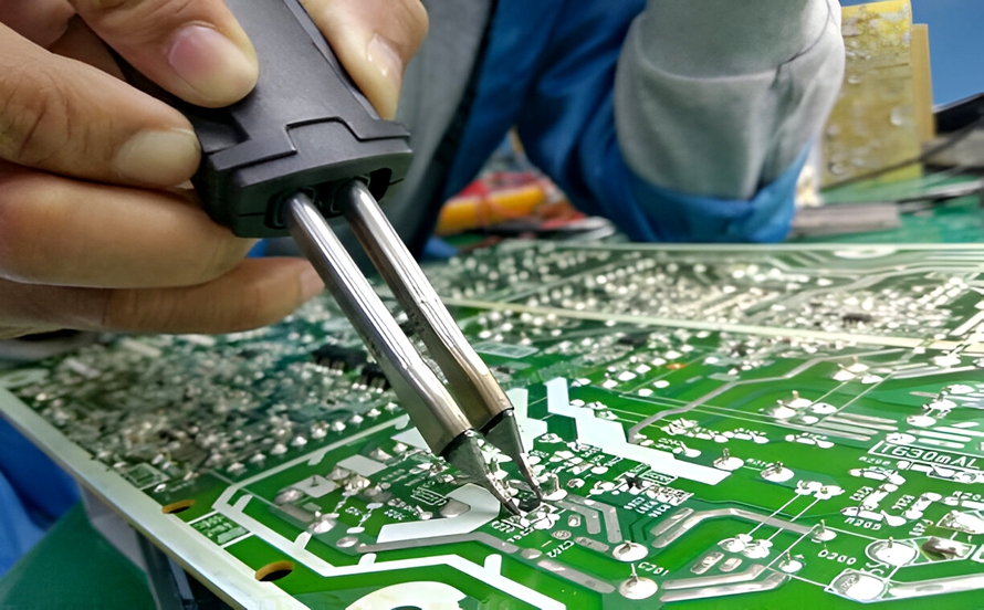
How to Desolder a Chip from a Circuit Board

How Do You Remove ICs and Hidden-Pad Components?

Select the removal process around the package connections. SOIC and QFP devices have visible perimeter leads, while QFN and BGA packages include solder joints beneath the body.

For visible-lead ICs, suitable hot-air equipment can heat the connections together. Some specialist removal methods use a compatible low-melting alloy, followed by thorough removal of that alloy before replacement.

Removing solder from visible leads does not prove that the entire package is released. An exposed thermal pad, concealed joint, adhesive, or underfill may still hold it in place.

A controlled IC removal process should address:

  • Package identification and orientation.
  • Moisture sensitivity and handling requirements.
  • Nozzle size and access around the component.
  • Board support and any required underside heating.
  • Temperature measurement at relevant locations.
  • Protection of nearby parts.
  • A lifting method that applies minimal force after release.

Hidden-joint packages require a process that heats the underside connections sufficiently while respecting the limits of the package and surrounding assembly.

Stop if the component resists lifting. Recheck the attachment and heating process before continuing. Increasing force can turn a replaceable component problem into damaged pads or broken internal connections.

For dense, underfilled, or high-value assemblies, professional rework offers better control over removal, replacement, and verification.
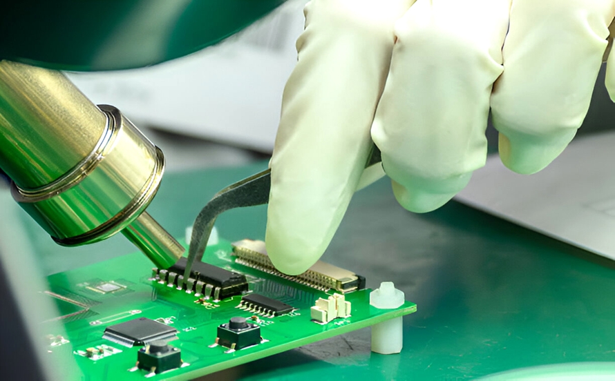
How to Desolder Circuit Board Components

How Do You Desolder an HDMI Port or Large Connector?

An HDMI port can combine fine signal contacts, large shield anchors, plastic insulation, and connections to substantial ground copper. The exact construction varies, so inspect the connector drawing and both sides of the board first.

Signal pins and mechanical anchors need separate attention. Fine contacts may release while the shield tabs remain firmly attached, or the reverse.

A practical removal plan is:

  1. Identify every attachment. Locate signal contacts, shield tabs, locating features, and any adhesive.
  2. Inspect surrounding parts. Check nearby plastic components, small passives, and cables.
  3. Choose the heating approach. Consider the connector’s thermal mass and whether controlled preheating is required.
  4. Release the connections. Use equipment suited to the fine contacts and larger anchors.
  5. Confirm full release. Lift only when every attachment permits removal with minimal force.
  6. Inspect the footprint. Check signal pads, anchor holes, traces, and nearby components.

Avoid levering the connector against the PCB. A loose-looking housing may still be attached by one contact or a concealed shield connection.

After removal, evaluate any damaged signal path before choosing a repair. HDMI uses high-speed differential connections, so a jumper that restores DC continuity may still alter signal behavior. Repair planning must consider geometry, electrical performance, mechanical strength, and access for inspection.
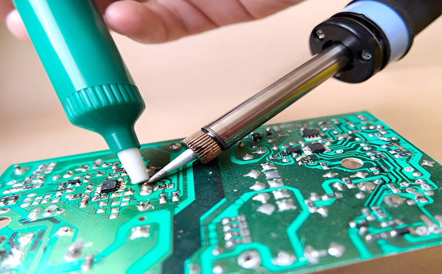
How to Desolder Small Components

What Common Mistakes Cause Desoldering Damage?

The most consequential mistakes involve moving a component before release, repeating ineffective heating, or overlooking part of the attachment.

  • Pulling while one joint remains solid: Transfers removal force into pads and traces. Confirm every connection is released.
  • Choosing a tiny tip for heavy copper: Limits heat transfer and encourages long contact. Match tip area and tool capacity to the joint.
  • Repeating unsuccessful heating cycles: Adds cumulative thermal exposure. Reassess the tool, contact, extraction, and board mass.
  • Pulling braid after it cools: Can pull copper away with the braid. Reheat and release it while molten.
  • Clearing holes with a drill: Can cut or remove plated copper. Use controlled heating and solder extraction.
  • Tapping the PCB to throw off solder: Scatters hot metal and stresses the assembly. Collect solder with a suitable removal tool.
  • Ignoring shield tabs or thermal pads: Leaves the component mechanically attached. Inspect the complete footprint.
  • Cleaning every flux with the same solvent: May leave residue or affect assembly materials. Follow the flux and material compatibility guidance.

Another common error is treating the highest available temperature as the quickest solution. Effective heat transfer comes from the whole setup: tool capacity, tip contact, joint condition, and board construction.

Stop and reassess when the process stops working. A change in equipment or technique is usually more useful than another identical heating attempt.

How Should You Inspect and Test the Board After Desoldering?

Allow the assembly to cool sufficiently for handling, then inspect the removal area under magnification. Compare it with the photographs taken before work.

Check both sides of the board where accessible:

  • Pads: Look for lifting, peeling, missing copper, or movement.
  • Traces: Inspect for scratches, breaks, and separation near pad edges.
  • Plated holes: Check for obstruction and visible barrel damage.
  • Laminate: Look for blistering, charring, or separation.
  • Adjacent parts: Check alignment, cracked bodies, disturbed joints, and heat effects.
  • Residue and debris: Locate solder balls, bridges, braid fragments, and cleaning residue.

Clean according to the flux manufacturer’s guidance and the assembly’s compatibility requirements. Isopropyl alcohol suits some residues, while other materials require a different process. Keep solvent away from ignition sources and allow the assembly to dry fully.

Before power-up, perform relevant electrical checks. These may include continuity along the affected net, checks for unintended connections between neighboring pads, and comparison of power-rail resistance with expected behavior. Low resistance alone does not establish a fault on every circuit.

Inspection after removal and verification after replacement are separate steps. Once the replacement is fitted, confirm orientation, solder-joint condition, and suitable functional performance. Hidden-joint packages may require additional inspection methods.

For production assemblies, record the board revision, component location, work performed, inspection result, and test outcome. This creates a useful reference if the same issue appears again.

When Should You Use Professional PCB Rework?

Professional rework is appropriate when successful removal depends on controlled thermal profiling, hidden-joint inspection, specialized pad repair, or verification beyond basic bench testing.

Consider it for BGA and QFN packages, fine-pitch connectors, multilayer boards with heavy copper, moisture-sensitive components, underfilled devices, and assemblies with existing pad or barrel damage.

The decision also depends on board value and application. A practice board offers room to learn. A medical, automotive, or other reliability-sensitive assembly needs a documented process and acceptance criteria suited to its use.

Where pad repair is permitted, evaluate the original connection, required current, mechanical loading, spacing, and signal function before selecting a repair method. A successful continuity reading alone does not establish that the repair is suitable for service.

If a PCB assembly project involves component replacement, assembly defects, or recurring soldering problems, contact EBest Circuit at sales@bestpcbs.com. Send clear photographs, the board revision, component reference and part number, quantities, and fault details so our engineering team can review the project requirements and available support.

FAQ About Circuit Board Desoldering

Q1: Does old solder have a higher melting point than fresh solder?
A1: Age alone does not define an alloy’s melting point, although oxidation and joint condition can make effective heating and wetting more difficult.

Q2: Can I mix leaded and lead-free solder during removal?
A2: Mixing alloys changes the joint composition, so use a method compatible with the assembly’s material, compliance, and reliability requirements.

Q3: Should I cut a faulty component’s leads before removing it?
A3: Cutting accessible leads can simplify removal when the component is being discarded, provided the cutting action places no damaging load on the PCB.

Q4: Can conformal coating stay in place during desoldering?
A4: Coating around the work area generally requires controlled local removal using a method suited to its chemistry and the underlying assembly.

Q5: Can a removed component be reused?
A5: Reuse depends on the component’s condition, thermal history, handling requirements, and the acceptance rules for the application.

Q6: Should a PCB be baked before rework?
A6: Baking depends on moisture exposure, component requirements, and the permitted temperature limits of the complete assembly.

Q7: Does solder wick expire?
A7: Solder wick has product-specific storage and shelf-life requirements because oxidation and flux condition affect its performance.
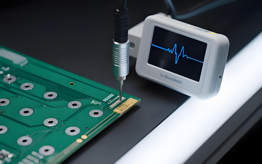
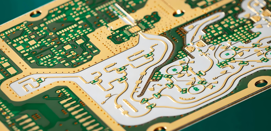
Impedance Control PCB

April 10th, 2026

If you’ve worked with high-frequency circuits or sensitive signals, you might have come across the term “impedance control.” Understanding and managing impedance can be the difference between a reliable design and one plagued by signal loss or interference.

Are You Facing These Challenges?

Many customers come to us after struggling with unstable signal performance, failed first builds, or mismatched stack-up assumptions.

Common Challenges

  • Signal reflection in high-speed traces
  • Differential pair mismatch
  • Unclear stack-up planning
  • Unexpected impedance deviation after fabrication
  • EMI issues caused by routing inconsistency
  • Difficulty finding a manufacturer that understands impedance requirements

Our Solution

We help review your layer structure, material selection, and trace geometry before production. With manufacturing-aware engineering support, we reduce the gap between design calculation and actual fabrication result.

Why Choose EBest Circuit for Impedance Control PCB?

Choosing the right manufacturer is important because controlled impedance is not only a calculation task. It is also a process control task. A good supplier needs to understand both design intent and manufacturing consistency.

What We Offer

  • Engineering support for stack-up review
  • Controlled impedance trace calculation support
  • Stable multilayer lamination process
  • In-process impedance monitoring
  • Support for high-speed and RF PCB projects
  • Fast prototype and production service
  • PCB and PCBA one-stop support

Our team works closely with customers during the early design stage to reduce risk before fabrication starts. That helps shorten revision cycles and improve project efficiency.

Impedance Control PCB

Impedance Control PCB Manufacturer

What is Impedance?

Impedance, in simple terms, is the opposition a circuit offers to the flow of alternating current (AC). It combines two elements: resistance, which is straightforward opposition, and reactance, which is the opposition due to capacitance and inductance. Together, they form impedance, usually measured in ohms (Ω).

In a PCB, impedance is vital because it affects how signals propagate through the traces. If the impedance isn’t controlled, it can lead to reflections, signal loss, or even total communication failure, especially in high-speed circuits.

What is Impedance Control PCB?

An impedance control PCB is a printed circuit board designed so that specific traces maintain a target impedance value throughout signal transmission. The purpose is to make sure signals travel with minimal loss, reflection, or distortion.

In PCB design, impedance is influenced by resistance, capacitance, and inductance. When signal speed rises, these factors become more critical. If impedance changes unexpectedly along the routing path, the signal quality can drop quickly. This is why controlled impedance is widely used in RF circuits, high-speed digital interfaces, and precision analog systems.

Common controlled impedance types include:

  • 50Ω single-ended impedance
  • 75Ω single-ended impedance
  • 90Ω differential impedance
  • 100Ω differential impedance
  • 120Ω differential impedance

The right target depends on your interface standard, material system, stack-up, and routing method.

What is Impedance Control PCB?

Why Is Controlled Impedance Important in PCB Design?

Controlled impedance matters because signal integrity depends on consistency. In high-speed designs, the copper trace is not just a conductor. It behaves like a transmission line. If the impedance of that transmission line does not match the system requirement, part of the signal energy reflects back toward the source.

This can lead to:

  • Signal reflection
  • Timing instability
  • Crosstalk
  • EMI problems
  • Higher bit error rates
  • Reduced communication reliability

For products using DDR memory, RF modules, antennas, automotive communication, industrial control, or high-speed connectors, impedance control is often not optional. It is part of the design foundation.

What Factors Affect PCB Impedance?

PCB impedance is not determined by one variable alone. It comes from the interaction of conductor geometry, laminate properties, and layer arrangement. Even a small change in fabrication can affect the final result.

1. Trace Width

Trace width is one of the most direct factors. A wider trace usually lowers impedance, while a narrower trace increases it. This is why impedance traces cannot be adjusted casually during layout optimization.

2. Copper Thickness

Copper thickness changes the effective conductor shape and resistance. Thicker copper can reduce impedance, but it also changes etching behavior and production tolerance.

3. Dielectric Constant (Dk)

The dielectric constant of the laminate affects electric field distribution and capacitance between the trace and reference plane. FR4 materials commonly show Dk values around 3.9 to 4.5, while PTFE materials are lower and often preferred for high-frequency applications.

4. Dielectric Thickness

The spacing between the signal trace and the reference plane has a strong effect on impedance. A thicker dielectric usually increases impedance, while a thinner dielectric lowers it.

5. Loss Tangent

Low-loss materials preserve signal energy better, especially in RF and high-speed applications. While loss tangent is not the only parameter that matters, it strongly affects real-world transmission quality.

6. Trace Coupling and Crosstalk

When traces are too close, coupling can change the expected impedance and create crosstalk. This is particularly important in dense differential pair routing.

7. Layer Stack-Up

In multilayer PCBs, impedance depends heavily on stack-up design. Signal layer position, plane continuity, dielectric thickness, and via transitions must all be considered together.

When Do You Need an Impedance Control PCB?

Not every board needs controlled impedance. For low-speed, low-frequency, or simple power control products, standard PCB design may be enough. But if your design includes fast signals or strict waveform requirements, controlled impedance becomes much more important.

You should consider impedance control for:

  • RF and microwave circuits
  • High-speed digital interfaces
  • DDR memory routing
  • USB, HDMI, PCIe, LVDS, and Ethernet designs
  • Differential pair signal routing
  • Sensitive analog signal paths
  • Long trace interconnects
  • Multi-layer signal-dense boards

In these applications, controlled impedance helps maintain cleaner transmission and more predictable electrical behavior.

What Is the Typical Impedance Tolerance of PCB?

Impedance tolerance refers to the acceptable variation between the target impedance and the actual measured result. In many PCB applications, the typical tolerance is ±10%. For more demanding products, tighter tolerances such as ±5% or even ±2% may be required.

A tighter tolerance usually requires:

  • More accurate material data
  • Better etching control
  • Stable lamination process
  • Precise stack-up construction
  • Reliable impedance coupon testing

This is why the manufacturer’s process capability matters just as much as the design itself.

How Is 100Ω Differential Impedance Controlled?

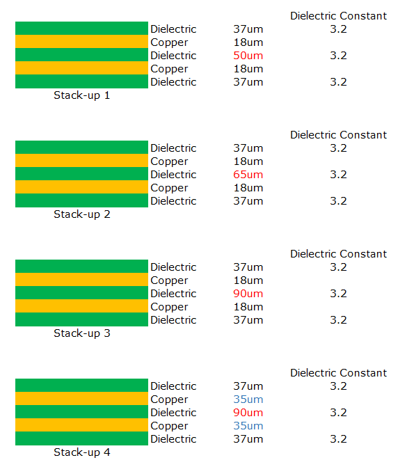
For 100Ω differential impedance, the process usually begins with stack-up definition and field-solver calculation. The dielectric thickness between layers, line width, and trace spacing must all be matched to the target value. Your original content provided example geometries for four different stack-up options, showing that trace width and spacing vary depending on the specific layer structure.

Example reference values include:

impedance control pcb stack up
  • Stack-Up 1: 70/130μm trace/space
  • Stack-Up 2: 95/140μm trace/space
  • Stack-Up 3: 125/130μm trace/space
  • Stack-Up 4: 105/150μm trace/space

During production, manufacturers normally establish process parameters after first article verification, then carry out random impedance checks during production and on finished boards.

Manufacturing Capabilities for Impedance Control PCB

At EBest Circuit (Best Technology), we support controlled impedance PCB manufacturing for a wide range of applications, from prototype builds to volume production.

Typical Capability Overview

ItemCapability
Board TypeRigid PCB, multilayer PCB, HDI PCB, RF PCB
Layer Count1–32 layers typical
Controlled Impedance TypeSingle-ended and differential
Common Target Values50Ω / 75Ω / 90Ω / 100Ω / 120Ω
Base MaterialsFR4, high-speed materials, RF laminates
Copper ThicknessStandard to heavy copper options
Impedance VerificationCoupon testing / in-process control
Application SupportRF, telecom, automotive, industrial, medical

Applications of Impedance Control PCB

Controlled impedance PCBs are widely used in products where signal integrity matters.

Typical applications include:

  • Communication equipment
  • RF modules
  • Automotive electronics
  • Medical devices
  • Industrial control systems
  • Network hardware
  • Embedded computing platforms
  • High-speed data transmission systems

As product speed and complexity continue to rise, controlled impedance is becoming a standard requirement in more electronic categories.

FAQs About Impedance Control PCB

1. What is the difference between impedance control and standard PCB design?

Standard PCB design may not define a strict trace impedance target. Impedance control PCB design requires specific trace width, spacing, material selection, and stack-up planning to achieve a defined impedance value.

2. Is FR4 suitable for impedance control PCB?

Yes. FR4 can be used for many controlled impedance applications, especially common digital designs. For higher frequencies or lower signal loss requirements, specialized materials may be a better choice.

3. What is the most common differential impedance value?

100Ω differential impedance is one of the most common targets, especially for many high-speed signal interfaces.

4. Can impedance control PCB reduce EMI?

Yes. Stable impedance routing can reduce reflections and signal discontinuities, which helps improve overall signal integrity and can support better EMI performance.

5. How is impedance tested during manufacturing?

Manufacturers commonly use impedance coupons and random process checks during production, followed by finished board verification.

6. What tolerance is usually acceptable?

A typical impedance tolerance is ±10%, while tighter requirements such as ±5% may be used in more demanding applications.

Get a Quote for Your Impedance Control PCB Project

If you are developing a high-speed or RF product, controlled impedance should be considered early in the design stage. A correct stack-up and manufacturable trace structure can save both time and revision cost later.

EBest Circuit (Best Technology) provides impedance control PCB manufacturing with engineering review, stack-up support, and reliable process control for demanding electronic applications.

Send us your Gerber files, layer stack-up, and impedance requirements, and our team will help you move your project forward with greater confidence.

High-Speed PCB

April 10th, 2026

High-speed PCB is used in electronic products where fast signal transmission, impedance stability, and low noise are essential to system performance. Once signal frequency rises, data rate increases, or edge transitions become faster, standard PCB layout rules are no longer enough. At that stage, the board must be engineered for signal integrity, EMI control, stack-up stability, and manufacturability.

EBest Circuit (Best Technology) provides high-speed PCB manufacturing for applications that require reliable transmission performance, including telecommunications, automotive electronics, aerospace systems, networking hardware, industrial control, medical electronics, and RF-related products. We support customers from prototype through volume production with practical engineering review, controlled process capability, and material options suited for high-speed designs.

Why Does High-Speed PCB Design Matter in Modern Electronics?

High-speed PCB design matters because fast signals do not behave like ordinary low-speed connections. As frequency increases and edge rates become sharper, the PCB trace begins to act like a transmission line. That means routing length, impedance variation, dielectric material, grounding, and via structure can all change the final electrical result.

If these factors are not handled correctly, the system may face signal reflection, crosstalk, EMI issues, timing mismatch, data errors, and unstable communication between devices. This is why high-speed PCB is not simply a faster version of a standard board. It is a different design discipline that requires electrical and manufacturing control from the beginning.

What Is a High-Speed PCB?

A high-speed PCB is a printed circuit board developed for circuits where signal integrity becomes a major design requirement. In many practical cases, high-speed conditions are associated with one or more of the following: operating frequency above 50 MHz, transmission rate above 1 Gbps, or rise and fall time below 500 ps.

In practical engineering terms, a board should be treated as high-speed when signal quality can be affected by impedance mismatch, trace discontinuity, return path interruption, material loss, delay mismatch, or noise coupling. Once any of these begin to affect performance, the PCB must be designed as a high-speed platform rather than a conventional one.

High-Speed PCB vs. Low-Speed PCB: What Is the Difference?

The real difference between a high-speed PCB and a low-speed PCB is not only clock frequency. The larger difference is how tightly the board must control electrical behavior to preserve signal quality and stable transmission.

ItemLow-Speed PCBHigh-Speed PCB
Signal behaviorLess sensitiveHighly sensitive
Impedance controlOften not criticalEssential
Trace routingBasic design rulesStrict electrical design rules
EMI concernLowerMuch higher
Material demandStandard FR4 often enoughMay require low-loss laminate
Timing controlLess criticalImportant for reliability
Stack-up planningFunctionalPerformance-driven

This comparison matters because many design issues appear when a board is still being treated like a conventional PCB even though the signals already behave like high-speed channels.

Are You Facing These High-Speed PCB Challenges?

Many OEMs, design houses, and sourcing teams run into the same issues when developing high-speed boards. The layout may look complete, but performance problems often appear during bring-up, test, or volume production.

  • Differential pair mismatch
  • Reflection caused by poor impedance control
  • Crosstalk between adjacent signal lines
  • EMI failure in dense multilayer boards
  • Excessive insertion loss at high frequency
  • Unstable routing performance between prototype and mass production
  • Material selection that does not match the actual signal requirement
  • Layout structures that are hard to manufacture consistently

These challenges are especially common in designs using PCIe, USB, Ethernet, HDMI, SATA, LVDS, and MIPI. When signal integrity, EMI, thermal behavior, power distribution, and component placement are not handled well, product performance can suffer quickly.

How Do We Help Solve High-Speed PCB Problems?

At EBest Circuit, we do more than fabricate copper patterns. We help align design intent with manufacturing reality so the finished board performs more predictably in actual use.

  • Material suggestion based on speed and loss targets
  • Stack-up review for impedance and return path stability
  • Controlled impedance manufacturing support
  • Routing manufacturability feedback
  • Process planning for multilayer and via structures
  • Prototype support for early validation
  • Stable transition from sample to production

This approach helps customers reduce design rework, shorten validation cycles, and improve consistency across builds.

What Materials Are Best for High-Speed PCB?

Dielectric material selection is essential because it affects how quickly and how cleanly signals travel through the PCB. In high-speed applications, lower dielectric constant materials are often preferred because they support faster signal propagation and lower loss.

MaterialTypical DkPerformance CharacteristicsTypical Applications
Standard FR4~4.5Cost-effective, suitable for moderate-speed designsGeneral electronics, some digital boards
Low-Loss FR4Lower than standard FR4Better signal performance, improved loss behaviorEmbedded systems, communication products
Rogers 4000 / 3000 Series~2.0–3.5Low loss, stable electrical performanceRF, telecom, automotive radar
PTFE~2.0–2.5Very low loss for very high-frequency applications5G, microwave, aerospace, radar

Material selection should not be based on cost alone. It should be based on the actual signal environment, channel loss budget, interface type, and board structure.

What Are the Most Important High-Speed PCB Design Rules?

High-speed PCB design works best when electrical rules are defined early and followed consistently throughout the layout. A strong design must balance signal performance with practical manufacturability.

1. Control Impedance Carefully
Critical traces must maintain consistent impedance from source to load. Any sudden change can create reflections and degrade signal quality.

2. Build the Right Stack-Up
A good stack-up places signal layers next to solid reference planes. This improves return path continuity and reduces EMI.

3. Keep Trace Length Practical
Longer routes increase delay and loss. Critical nets should stay as short and direct as possible.

4. Reduce Crosstalk
Parallel routing should be limited, and spacing should be sufficient to reduce coupling between signal lines.

5. Route Differential Pairs Correctly
Differential pairs need consistent spacing, matched length, and stable reference conditions.

6. Manage Via Effects
Vias add parasitic inductance and capacitance. Poor via usage can hurt signal quality, especially in dense high-speed layouts.

7. Improve Power Integrity
Stable power delivery is important because high-speed ICs are sensitive to supply noise.

8. Optimize Component Placement
Key components should be placed to reduce routing complexity and improve signal path quality.

Which Interfaces Require High-Speed PCB Design?

Many modern electronic products rely on interface standards that demand strong high-speed layout and manufacturing control.

  • PCIe for high-speed peripheral data transfer
  • USB for fast communication and storage
  • Ethernet for networking up to high data rates
  • HDMI for high-bandwidth video and audio
  • SATA for storage communication
  • LVDS for displays and cameras
  • MIPI for mobile and embedded camera or display systems

When these interfaces are present, stack-up design, impedance control, pair routing, and connector transition quality become much more important.

How Is a High-Speed PCB Manufactured?

The manufacturing flow of high-speed PCB is more demanding than standard PCB because even small process variation can influence electrical performance. A reliable process must support both structural accuracy and repeatable signal behavior.

1. Material Selection
The correct laminate is chosen based on dielectric constant, signal frequency, and loss requirement.

2. Layer Stack-Up Design
Signal, power, and ground layers are arranged to support impedance targets and EMI control.

3. Trace Width Calculation and Impedance Control
Trace width and spacing are verified to match single-ended or differential impedance requirements.

4. Lamination
Multilayer panels are bonded under controlled pressure and temperature.

5. Drilling and Via Formation
Through holes, blind vias, buried vias, or microvias are created based on design need.

6. Copper Plating
Plating forms conductive connections between layers and helps ensure electrical reliability.

7. Etching
Precision etching defines trace width and spacing, which directly affects impedance.

8. Solder Mask and Silkscreen
Protective coating and identification marking are added.

9. Surface Finish
Common finish options include ENIG, OSP, and immersion silver.

10. Testing and Inspection
Final checks confirm electrical continuity, dimensional control, and manufacturing quality.

Why Choose EBest Circuit as Your High-Speed PCB Manufacturer?

For high-speed PCB projects, manufacturing experience matters because electrical performance depends on how well the design is translated into the real board. A supplier that understands only fabrication may miss what actually matters to the final product.

  • Support for impedance-controlled high-speed PCB fabrication
  • Experience with FR4, low-loss materials, Rogers, and PTFE-based builds
  • Engineering review for stack-up and manufacturability
  • Prototype and production support
  • Stable multilayer process control
  • One-stop PCB and PCBA support when required
  • Application experience across telecom, automotive, aerospace, industrial, and RF-related products

We focus on helping customers improve both performance and production stability, not only getting the board built.

What Applications Use High-Speed PCB?

High-speed PCBs are used in many industries where fast signal transmission and reliable electrical performance are essential.

  • Telecommunications equipment
  • Automotive electronics and radar systems
  • Aerospace electronics
  • 5G infrastructure
  • Data centers
  • Defense systems
  • Medical devices
  • Networking equipment
  • RF and microwave systems
  • Industrial electronic control products

As data rates continue to rise across industries, high-speed PCB design is becoming a standard requirement in more product categories.

What Should You Look for in a High-Speed PCB Supplier?

If you are selecting a manufacturer, it helps to evaluate more than price and lead time. A better supplier should also understand the electrical side of the board.

  • Knowledge of signal integrity basics
  • Material options for different speed ranges
  • Controlled impedance capability
  • Multilayer stack-up support
  • Stable drilling, plating, and etching control
  • Clear communication during DFM review
  • Reliable prototype-to-production consistency

This reduces the chance of performance drift between sample builds and mass production orders.

Need a High-Speed PCB Quote for Your Project?

If your design includes fast data channels, impedance-sensitive routing, or multilayer architecture with demanding electrical requirements, we can help. EBest Circuit (Best Technology) provides high-speed PCB support from engineering review through fabrication and delivery.

Send us your Gerber files, stack-up, impedance requirements, or project specifications, and we will review the best manufacturing solution for your application.

FAQ About High-Speed PCB

1. What is considered a high-speed PCB?
A PCB is commonly treated as high-speed when the operating frequency is above 50 MHz, the data rate exceeds 1 Gbps, or the signal rise and fall time is below 500 ps.

2. Can FR4 be used for high-speed PCB?
Yes. FR4 can be used in some moderate-speed applications. For higher-frequency or lower-loss designs, Rogers or PTFE-based materials may be more suitable.

3. Why is impedance control important in high-speed PCB?
Impedance control helps reduce signal reflection and preserves waveform integrity during fast transmission.

4. What interfaces usually need high-speed PCB design?
PCIe, USB, Ethernet, HDMI, SATA, LVDS, and MIPI are common examples.

5. What surface finishes are used for high-speed PCB?
Common options include ENIG, OSP, and immersion silver.

6. Which industries use high-speed PCBs?
Telecommunications, automotive, aerospace, 5G, medical, defense, networking, and RF-related industries all use high-speed PCBs.

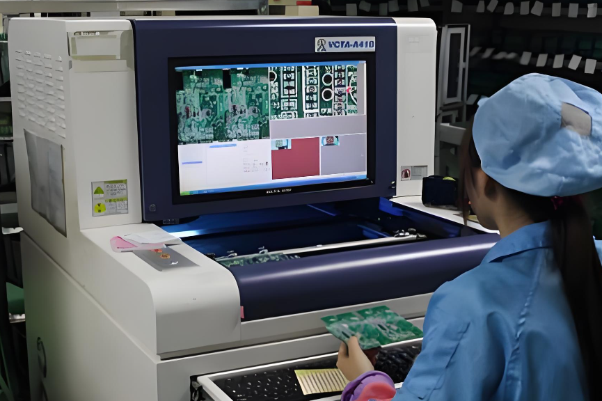
Automated Optical Inspection AOI Inspection for PCB & PCB Assembly

April 10th, 2026

What Is AOI Inspection?

AOI inspection, short for Automated Optical Inspection, is a quality control method used in PCB and PCBA manufacturing to automatically detect visual defects on circuit boards. It relies on high-resolution cameras, controlled lighting systems, and image processing algorithms to evaluate whether a board meets predefined standards.

In modern electronics manufacturing, AOI is not just an optional inspection step. It is a core process that ensures assembly accuracy, especially in high-density SMT production environments where manual inspection becomes inefficient and inconsistent.

Unlike traditional visual inspection performed by operators, AOI systems provide repeatable and objective results. They compare the inspected PCB against a reference, such as a “golden board” or CAD data, to identify deviations.

AOI Inspection

How Does AOI Inspection Work in PCB Assembly?

AOI inspection follows a structured process that combines imaging technology with intelligent comparison algorithms.

Step 1: Image Capture

High-speed cameras scan the PCB using multiple light sources. These include white light, RGB, and angled lighting to highlight solder joints and component edges.

Step 2: Reference Matching

The system compares captured images with:

  • Golden board samples
  • CAD / Gerber data
  • Component libraries

Step 3: Defect Detection

Software identifies deviations such as placement errors or solder defects.

Step 4: Classification & Output

Detected issues are categorized and displayed for operator review or automatically logged into MES systems.

Why Is AOI Inspection Important in SMT Production?

In modern SMT environments, defect tolerance is extremely low due to miniaturization and high-density layouts.

AOI inspection directly improves:

  • First Pass Yield (FPY) by detecting issues early
  • Process stability through continuous feedback
  • Cost control by reducing rework and scrap
  • Production efficiency with high-speed inspection

From an engineering standpoint, AOI is not just an inspection tool. It is a process optimization system that helps identify root causes such as stencil wear, placement deviation, or reflow inconsistencies.

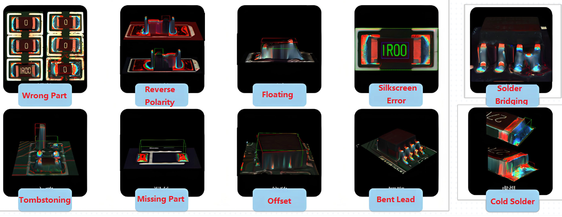
What Defects Can AOI Inspection Detect?

AOI inspection is designed to identify visible defects related to component placement and solder quality. These defects typically include:

  • Missing components
  • Incorrect components
  • Misaligned or shifted components
  • Wrong polarity (especially for diodes and ICs)
  • Tombstoning (one side lifted)
  • Solder bridging
  • Insufficient solder
  • Excess solder
  • Open solder joints
  • Lifted leads
  • Surface contamination or scratches
What Defects Can AOI Inspection Detect?

These defects are common in SMT assembly and can significantly affect product performance.

However, AOI focuses on surface-level inspection. It is most effective for defects that can be visually detected. For hidden defects, additional inspection methods are required.

Where Is AOI Inspection Used in the Manufacturing Process?

AOI inspection can be deployed at multiple stages of PCB assembly. Each stage serves a different purpose.

Post-reflow AOI

This is the most common AOI stage. It inspects solder joints and component positions after reflow. Most solder-related defects are identified here.

Wave solder AOI

For through-hole components, AOI can be used after wave soldering to inspect solder quality and component insertion.

Final AOI inspection

Some manufacturers include a final AOI step to ensure no defects were missed earlier.

In practice, many high-end SMT lines use multiple AOI checkpoints to maximize defect coverage and process control.

What Are the Main Benefits of AOI Inspection?

AOI inspection delivers measurable benefits across production efficiency and product quality.

  • Unlike manual inspection, AOI provides consistent results regardless of operator fatigue or experience.
  • AOI systems can inspect thousands of components per second, supporting high-volume production.
  • By using AOI inspection, defects are identified immediately, reducing downstream failures.
  • Fewer operators are required for inspection tasks
  • Inspection data can be analyzed to improve process parameters and prevent recurring issues.

For manufacturers aiming to scale production while maintaining quality, AOI is a fundamental investment.

What Is the Difference Between 2D AOI and 3D AOI Inspection?

AOI systems are typically categorized into 2D and 3D technologies.

Feature2D AOI3D AOI
Inspection methodImage-basedHeight + image analysis
Solder evaluationLimitedAccurate volume measurement
AccuracyModerateHigh
CostLowerHigher
ApplicationStandard SMTHigh-density / complex boards

2D AOI relies on color and contrast to detect defects. It is suitable for most standard applications.

3D AOI adds height measurement using techniques such as structured light or laser scanning. This allows it to evaluate solder volume and detect defects that 2D systems may miss.

For advanced applications such as fine-pitch components or reflective surfaces, 3D AOI provides better reliability.

AOI Inspection vs AXI vs Manual Visual Inspection

Different inspection methods serve different purposes in PCB assembly.

AOI vs AXI (Automated X-ray Inspection)

AOI inspects visible surfaces, while AXI is used for hidden structures such as BGA solder joints. AXI can detect voids and internal defects that AOI cannot see.

AOI vs manual inspection

Manual inspection depends on human judgment and is prone to inconsistency. AOI offers higher speed and repeatability.

In practice, these methods are complementary. A typical high-reliability production line may use:

  • SPI (Solder Paste Inspection)
  • AOI
  • X-ray inspection
  • Functional testing

This layered approach ensures comprehensive quality control.

What Are the Limitations of AOI Inspection?

While AOI is powerful, it has certain limitations. It cannot effectively inspect hidden solder joints, such as those under BGA components. It also depends heavily on programming quality. Poorly optimized programs can result in false calls or missed defects.

Reflective surfaces and complex geometries can sometimes challenge the system. In addition, AOI requires proper lighting and calibration to maintain accuracy.

Why Choose EBest Circuit (Best Technology) for AOI Inspection and PCBA Quality Control?

At EBest Circuit, AOI inspection is fully integrated into the PCB assembly workflow to ensure consistent quality at every stage.

Key advantages include:

  • Advanced AOI systems supporting both prototype and mass production
  • Multi-stage inspection strategy (pre-reflow and post-reflow)
  • Integration with MES for full traceability
  • Experienced engineering team for AOI programming optimization
  • Combined inspection capabilities including X-ray, SPI, ICT, and functional testing
  • Fast feedback loop to improve yield and reduce defects

With nearly 20 years of PCBA experience, EBest supports industries requiring high reliability, including automotive, medical, and industrial electronics.

FAQs About AOI Inspection

1. What is AOI inspection in PCB assembly?

AOI inspection is an automated method that uses cameras and software to detect visual defects on PCBs. It helps ensure component placement accuracy and solder quality.

2. What is AOI inspection used for?

AOI inspection is used to automatically detect visible defects in PCB assembly, including component placement errors and soldering issues, ensuring product quality and consistency.

3. Can AOI detect all PCB defects?

No, AOI detects only visible defects. Hidden issues such as BGA solder joints require X-ray inspection.

4. Is AOI better than manual inspection?

Yes, AOI is faster, more consistent, and less dependent on human factors, making it more suitable for high-volume production.

5. Where should AOI be placed in SMT lines?

AOI is typically used both before reflow (placement check) and after reflow (solder inspection) for optimal results.

6. What is the difference between 2D and 3D AOI?

2D AOI uses image comparison, while 3D AOI measures height and volume, providing more accurate solder inspection.

Ready to Improve Your PCB Assembly Quality?

If you are facing challenges such as inconsistent quality, high rework rates, or hidden defects in SMT production, integrating AOI inspection is a proven solution.

EBest Circuit offers one-stop PCB and PCBA services, combining advanced AOI inspection with full-process quality control.

Get started today:

  • Send your Gerber & BOM for review
  • Receive fast DFM + inspection feedback
  • Support from prototype to mass production

Contact: sales@bestpcbs.com

Single Sided PCB

April 10th, 2026

Single sided PCB is one of the most practical board types for straightforward electronic designs. With copper circuitry on only one side of the substrate, it offers a simple structure, stable performance, and competitive manufacturing cost for high-volume applications.

At EBest Circuit, we provide custom single sided PCB manufacturing for customers who need dependable quality, fast turnaround, and responsive engineering support. From prototype runs to volume production, our team helps you move from design to delivery with better efficiency and fewer production concerns.

What Is a Single Sided PCB?

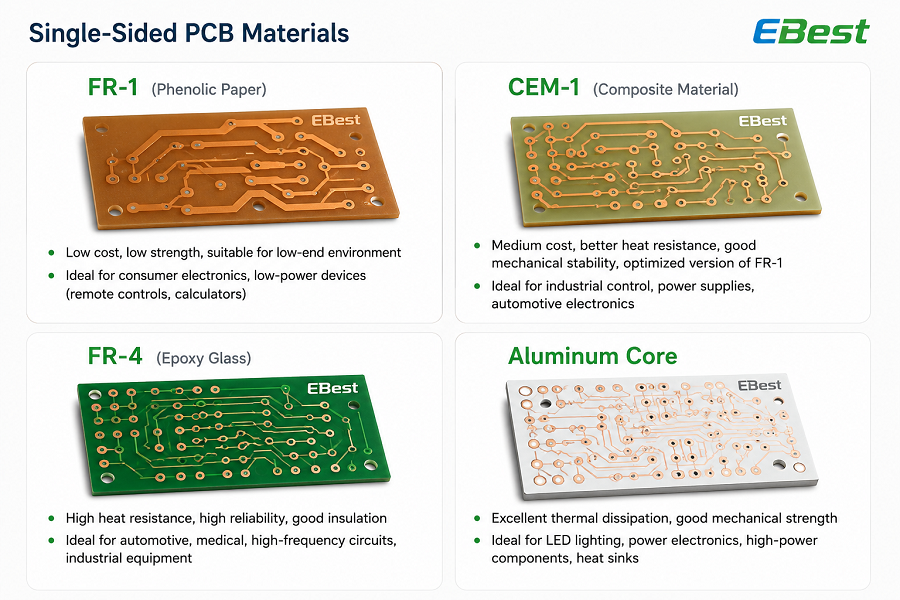
A single sided PCB, also called a 1 layer PCB, is a printed circuit board with conductive copper traces on only one side of the substrate. All components are mounted on the same side, and the electrical paths are routed through a single copper layer.

This is one of the most basic and widely used PCB structures in electronics. Because of its simple layout and efficient production process, a single sided PCB is often chosen for products that do not require complex routing or high component density.

In most cases, the base material is FR4 or another insulating substrate, with a copper foil laminated on one side. The copper is then etched to form the required circuit pattern.

Single sided PCBs are commonly used in:

  • LED lighting products
  • Power supplies
  • Consumer electronics
  • Calculators
  • Simple control boards
  • Household appliances

For straightforward electronic designs, this board type remains a practical and cost-efficient solution.

Single Sided PCB

Our Single Sided PCB Manufacturing Capabilities

At EBest Circuit, we support custom PCB manufacturing with a strong focus on manufacturability, quality consistency, and customer-specific requirements. Our single sided PCB service is suitable for both basic commercial products and more specialized industrial applications.

Available Options Include:

  • Custom board dimensions
  • FR4 and other substrate selections
  • Different copper thickness options
  • Multiple solder mask colors
  • Surface finishes based on assembly and performance needs
  • Prototype, small batch, and mass production support
  • Through-hole and SMT compatible designs

We review each project based on the intended application, assembly method, and electrical requirements, helping customers choose a more suitable board configuration before production starts.

How Is a Single Sided PCB Manufactured?

The manufacturing process of a single sided PCB is relatively direct, which is one reason it remains popular for high-volume production and cost-sensitive projects.

1. Circuit Design and Layout

The process starts with PCB design. Engineers create the circuit layout using CAD software, defining component placement, trace routing, hole positions, and board dimensions.

A clean layout is especially important in a 1 layer PCB because routing space is limited. Good design at this stage helps reduce manufacturing risk and improves final board performance.

2. Substrate Preparation

After the design is finalized, the insulating substrate is prepared and cut to the required board size. FR4 is one of the most common materials used, although other substrates may be selected depending on the application.

3. Copper Lamination

A thin copper layer is laminated onto one side of the substrate. This copper layer will later be patterned into the conductive traces needed for the circuit.

4. Photoresist Coating

A light-sensitive photoresist material is applied over the copper surface. This coating protects the intended circuit pattern during the etching stage.

5. Exposure and Development

The board is exposed to UV light through a film or mask containing the circuit image. After development, the unwanted photoresist is removed, leaving the desired copper pattern protected.

6. Etching

The exposed copper is removed through a chemical etching process. Only the protected copper remains, creating the final conductive pathways.

7. Solder Mask Application

A solder mask is applied over the board surface to protect the copper traces from oxidation and reduce the risk of solder bridging during assembly. Green is the most common color, though other colors are also available.

8. Component Assembly and Soldering

Electronic components are mounted in their designated positions. Depending on the design, this may involve SMT assembly or through-hole soldering.

9. Testing and Inspection

The finished board goes through electrical testing and quality inspection to confirm continuity, functionality, and manufacturing accuracy. This step helps ensure the PCB performs as designed before shipment.

What Is a Double Sided PCB?

A double sided PCB has conductive copper layers on both sides of the substrate. This structure allows components and traces to be placed on the top and bottom surfaces, giving designers more routing flexibility.

To connect the two copper layers, the board uses plated through holes (PTH) or vias. These conductive holes allow electrical signals to move from one side of the board to the other.

Because of this added routing capability, double sided PCBs are suitable for more complex circuits than single sided boards. They are widely used in:

  • Automotive electronics
  • Communication equipment
  • Industrial control systems
  • Power electronics
  • Instrumentation devices

A double sided PCB is often the next step when a single-layer layout can no longer support the required circuit density.

What Is a Double Sided PCB?

What Is a Double Sided PCB?

Single Sided PCB vs Double Sided PCB

Choosing the right board type depends on circuit complexity, layout density, and budget expectations. For many buyers, the first comparison is between single sided PCB and double sided PCB.

ItemSingle Sided PCBDouble Sided PCB
Copper Layers12
Circuit ComplexityLowMedium
Routing FlexibilityLimitedHigher
Manufacturing CostLowerHigher
Production ProcessSimplerMore complex
Through Hole ConnectionNot required for interlayer routingRequired for layer connection
Typical ApplicationsSimple electronicsMore compact and functional products

If the layout can be completed on one layer without excessive jumpers or routing compromise, single sided PCB is usually the more economical option. When routing space becomes tight, double sided PCB offers greater design freedom.

Single Sided PCB vs Multilayer PCB

A multilayer PCB includes three or more conductive layers and is built for more advanced circuits. Compared with a 1 layer PCB, it supports higher density routing, better signal management, and more compact product design. However, many products do not need that level of complexity.

A single sided PCB is usually the better fit when you need:

  • A cost-sensitive board solution
  • Simple electrical architecture
  • Faster production
  • Easier inspection and assembly
  • Stable supply for repetitive orders

A multilayer PCB is more appropriate when the project involves:

  • High-speed signal routing
  • Compact board area with dense components
  • Strict EMI or impedance requirements
  • More advanced system integration

The best choice is not always the most complex structure. It is the one that matches your product’s real design needs.

Single Sided PCB vs Multilayer PCB

Single Sided PCB vs Multilayer PCB

How Thick Is a Single Sided PCB?

The thickness of a single sided PCB depends on the application, mechanical requirements, and manufacturing specification. In many cases, the common finished thickness range is:

  • 0.6 mm
  • 0.8 mm
  • 1.0 mm
  • 1.2 mm
  • 1.6 mm

Among these, 0.8 mm to 1.0 mm is often selected for standard applications because it provides a good balance between strength, weight, and cost.

PCB thickness usually includes:

  • Base substrate thickness
  • Copper thickness
  • Solder mask and surface finish contribution

Thicker boards may be preferred when stronger mechanical support is needed. Thinner boards may be selected for compact or lightweight products.

Choosing the right board thickness should always be based on the end-use environment, assembly method, and overall design requirements.

How to Choose the Right PCB Type for Your Project?

Selecting between a single sided PCB, double sided PCB, and multilayer PCB depends on several practical factors.

Choose a Single Sided PCB If:

  • Your circuit is simple
  • Cost control is a priority
  • Component density is low
  • Fast fabrication is important
  • The product is mature and stable

Choose a Double Sided PCB If:

  • You need more routing space
  • Components must be mounted on both sides
  • A single-layer layout becomes too crowded
  • The product requires moderate complexity

Choose a Multilayer PCB If:

  • The design includes complex signal routing
  • Space is limited
  • High-speed or high-performance performance matters
  • EMI control and signal integrity are critical

A good PCB supplier can review your files and recommend the most suitable stack-up and board type before production begins.

Common Applications of Single Sided PCB

Single sided PCBs are still widely used across many industries because they serve a large number of standard electronic functions efficiently.

Typical applications include:

  • LED modules and lighting controls
  • AC/DC power boards
  • Battery management in simple devices
  • Consumer appliance boards
  • Small motor control circuits
  • Basic sensor and interface boards
  • Chargers and adapters
  • Industrial support electronics

For buyers looking for a dependable and cost-conscious board platform, this type of PCB remains highly relevant.

What Files Do We Need for Quotation?

To provide an accurate quotation and technical review, it is helpful to share:

  • Gerber files
  • Drill files
  • PCB specification details
  • Board size and thickness
  • Copper thickness requirement
  • Surface finish requirement
  • Quantity demand
  • Assembly files if PCBA is needed

If your files are still under preparation, you can also send the available design information first. Our team can help review the project and advise on the next step.

Get a Quote for Single Sided PCB Manufacturing

Looking for a reliable single sided PCB manufacturer for your next project?

EBest Circuit supports custom 1 layer PCB fabrication with responsive engineering service, practical lead times, and dependable production quality. Whether you need a quick prototype or a stable supplier for volume orders, we are ready to support your project.

Send us your design files and specifications for a fast review and quotation.

Email: sales@bestpcbs.com

Rigid Flex Circuit

April 10th, 2026

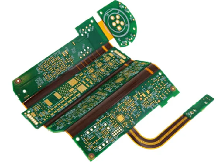
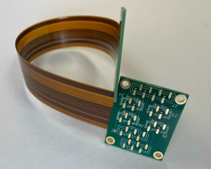
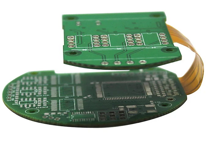
Rigid flex circuit is a PCB structure that combines rigid board sections and flexible circuit layers into one integrated unit. It offers the strength of rigid FR4 boards and the space-saving advantage of flexible circuits. Compared with a standard flex PCB with stiffeners, a true rigid flex board is built with plated through holes (PTH) that electrically connect the rigid and flexible layers inside the structure.

Rigid flex PCBs are widely used in medical devices, aerospace electronics, industrial controls, automotive systems, and advanced consumer products where stable performance and compact structure are required.

What Is a Rigid Flex Circuit?

A rigid flex circuit is a hybrid PCB made by laminating rigid substrates and flexible substrates into one board structure. The rigid sections support component mounting, while the flexible sections allow bending or folding during installation.

This design helps engineers reduce assembly size, simplify internal wiring, and improve product reliability. Instead of using multiple separate boards connected by cables or connectors, a rigid flex PCB combines these functions into one integrated interconnection platform.

Main Features of Rigid Flex PCB

  • Combines rigid and flexible substrates in one board
  • Uses plated through holes for internal electrical interconnection
  • Supports compact and three-dimensional assembly design
  • Reduces connectors, cables, and manual soldering points
  • Improves reliability in high-vibration and limited-space applications
Rigid Flex Circuit

Rigid Flex Circuit

Our Typical Project Cases

Case 1 – Medical Portable Monitoring Device Rigid Flex PCB

Application: Portable medical monitoring system

Board Type: 6 Layer Rigid Flex PCB

Material: FR4 + Polyimide

Surface Finish: ENIG

Key Requirement: Compact size, stable signal, high reliability

Medical Portable Monitoring Device Rigid Flex PCB

Case 2 – Automotive Camera Module Rigid Flex PCB

Application: Automotive camera system

Board Type: 4 Layer Rigid Flex PCB

Material: High Tg FR4 + Polyimide

Surface Finish: ENIG

Key Requirement: Vibration resistance, compact structure

Automotive Camera Module Rigid Flex PCB

Case 3 – Industrial Control System Rigid Flex PCB

Application: Industrial control module

Board Type: 8 Layer Rigid Flex PCB

Material: FR4 + Polyimide

Surface Finish: ENIG

Key Requirement: High density routing, stable interconnection

Industrial Control System Rigid Flex PCB

Case 4 – Consumer Electronics Folding Device Rigid Flex PCB

Application: Foldable consumer electronic device

Board Type: 4 Layer Rigid Flex PCB

Material: FR4 + Polyimide

Surface Finish: ENIG

Key Requirement: Repeated bending, compact layout

Consumer Electronics Folding Device Rigid Flex PCB

Rigid Flex PCB vs. Flex PCB with Stiffener

A rigid flex circuit is different from a flex PCB with FR4 or polyimide stiffeners.

In a flex PCB with stiffener, the stiffener is added only for local support. It is usually attached by adhesive and does not provide plated electrical interconnection between layers.

In a rigid flex PCB, the rigid and flexible sections are laminated into one complete structure, and the layers are electrically connected through plated through holes. This gives the board stronger structural integrity and better long-term reliability.

Key Difference

ItemRigid Flex CircuitFlex PCB with Stiffener
StructureIntegrated rigid and flex laminateFlex circuit with added support layer
Electrical InterconnectionYes, through plated holesNo plated interconnection through stiffener
Mechanical StabilityHigherModerate
Assembly IntegrationBetterLimited
Typical UseHigh-reliability compact productsLocal reinforcement only

Our Rigid Flex PCB Manufacturing Capabilities

Below is a typical reference table for custom rigid flex PCB manufacturing capability.

ParameterTypical Capability
Rigid Flex StructureSingle-sided, double-sided, multilayer rigid flex
Base MaterialsFR4 + Polyimide
Layer Count2L to 50L
Rigid Layer MaterialStandard FR4 / High Tg FR4
Flexible Layer MaterialPolyimide (PI)
Copper Thickness0.5 oz to 4 oz
Board ThicknessCustom build-up
Flex ThicknessBased on stack-up design
Min Line / Space4/4 mil
Min Drill Hole0.2 mm
Surface FinishENIG, HASL, OSP, Immersion Tin, Immersion Silver
Solder MaskGreen, Black, White, Red, Blue, Yellow
CoverlayYellow / Black / White
Stiffener OptionFR4, PI, Stainless Steel
Impedance ControlSupported
Via TypePTH, blind via, buried via, microvia based on design
Assembly ServicePCB fabrication + SMT assembly
Production TypePrototype to mass production
Assembly SupportSMT, THT, mixed technology assembly
File SupportGerber, drill file, stack-up, assembly drawing, BOM

Common Rigid Flex Stack-Ups

Rigid flex PCB structures are usually designed as multilayer constructions. The final stack-up depends on routing density, bend radius, thickness target, and mechanical design requirements.

4 Layer Rigid Flex

Option 1

  • 1L FR4
  • 2L FPC
  • 1L FR4

Option 2

  • 2L FR4
  • 2L FPC

6 Layer Rigid Flex

Option 1

  • 2L FR4
  • 2L FPC
  • 2L FR4

Option 2

  • 1L FR4
  • 4L FPC
  • 1L FR4

8 Layer Rigid Flex

Option 1

  • 2L FR4
  • 4L FPC
  • 2L FR4

Option 2

  • 1L FR4
  • 6L FPC
  • 1L FR4

Option 3

  • 2L FPC
  • 4L FR4
  • 2L FPC

Option 4

  • 1L FPC
  • 6L FR4
  • 1L FPC

Special Rigid Flex Structures for Custom Applications

Besides standard multilayer designs, some projects require custom rigid flex configurations for special packaging or functional needs.

2 Layer Rigid Flex

  • 1L FR4
  • 1L FPC

3 Layer Rigid Flex

Option 1

  • 1L FR4
  • 1L FPC
  • 1L FR4

Option 2

  • 1L FPC
  • 1L FR4
  • 1L FPC

These special designs are often used in compact electronic modules where a simple but integrated board structure is needed.

Design and Manufacturing Considerations

A reliable rigid flex PCB depends not only on layout, but also on manufacturability planning. Early engineering review can help avoid cracking, delamination, poor bend performance, and assembly issues.

Key Points to Consider

  • Stack-up design between rigid and flex areas
  • Bend radius and bending direction
  • Copper balancing in flex zones
  • Coverlay opening design
  • Stiffener placement
  • Hole location near bend areas
  • Final thickness control
  • Component placement on rigid sections only
  • Impedance and signal path planning for high-speed designs

A good rigid flex supplier should review these details before production, not after problems appear.

Typical Applications of Rigid Flex PCB

  • Medical monitoring and portable diagnostic devices
  • Aerospace and defense electronics
  • Industrial control systems
  • Automotive electronic modules
  • Cameras and optical devices
  • Consumer electronics with compact internal layouts

Why Work With EBest Circuit (Best Technology) for Rigid Flex PCB?

EBest Circuit provides custom rigid flex PCB manufacturing for projects that require compact structure, stable interconnection, and reliable quality. With over 20 years of PCB experience, we support customers from design review to fabrication and assembly.

What We Offer

  • Custom rigid flex PCB fabrication
  • Stack-up review and DFM support
  • PCB and PCBA one-stop service
  • Prototype and volume production support
  • Material and process suggestion based on application
  • Fast response for RFQ and engineering questions

Our engineering team understands the practical challenges behind rigid flex structures and helps customers improve both design feasibility and production stability.

What Files Are Recommended for RFQ?

To speed up quotation and technical review, it is helpful to provide:

  • Gerber files
  • Drill files
  • Stack-up information
  • Fabrication drawing
  • Assembly drawing
  • BOM list
  • Pick and place file if assembly is needed

Clear documentation helps reduce back-and-forth communication and improves quote accuracy.

FAQs

1. What is the minimum bend radius for rigid flex PCB?

The bend radius depends on the flex thickness and copper structure. A common guideline is:

  • Single-layer flex: 6–10 × thickness
  • Double-layer flex: 10–15 × thickness
  • Multilayer flex: 15–20 × thickness

Proper bend radius design is critical to prevent copper cracking or delamination during use.

2. Can components be placed on the flexible area?

In most cases, components should be mounted only on the rigid sections.

Placing components on flex areas is possible in special designs, but it requires careful reinforcement, controlled bending conditions, and additional manufacturing considerations. For standard designs, keeping components on rigid areas improves reliability and assembly stability.

3. What materials are used in rigid flex PCB?

Rigid flex circuits typically use:

  • Rigid layers: FR4 or high Tg FR4
  • Flexible layers: Polyimide (PI)
  • Coverlay: Polyimide film with adhesive
  • Stiffeners: FR4, PI, or stainless steel

Material selection depends on temperature requirements, bending cycles, and electrical performance.

4. How many bending cycles can a rigid flex PCB withstand?

The bending life depends on the design and materials. With proper design, rigid flex circuits can withstand thousands to millions of bending cycles.

Key factors include:

  • Copper thickness
  • Flex layer structure
  • Bend radius
  • Material quality

Engineering optimization is important for applications requiring repeated movement.

Get a Quote for Your Rigid Flex Circuit Project

Looking for a reliable rigid flex PCB manufacturer for your next project? Best Technology can support your design with engineering review, custom stack-up guidance, and stable production service.

Send your Gerber files, stack-up details, or project requirements to sales@bestpcbs.com for quotation and technical support.

RF Board

April 10th, 2026

What Is an RF PCB?

RF board, or Radio Frequency Printed Circuit Board, is engineered for circuits operating at high frequencies where signal integrity becomes highly sensitive to material properties. Typical RF designs work in the range of 300 MHz to 3 GHz, and many advanced systems extend far beyond this.

At these frequencies, standard FR4 materials often fail to maintain stable dielectric performance and low signal loss. As a result, specialized high frequency laminates are required. RF PCBs are therefore built using materials with low dielectric loss (Df) and stable dielectric constant (Dk) to ensure consistent signal transmission.

RF board is ideal for applications with higher operating frequency requirements. Right now, we normally use following material:

These boards are widely used in applications such as:

  • Wireless communication systems
  • RF antennas and modules
  • Automotive radar (ADAS)
  • Satellite and aerospace electronics
  • Microwave devices
  • IoT and high-speed signal systems

Why Use RF PCB Instead of Standard FR4?

FR4 is cost-effective and widely used, but its dielectric properties vary significantly at high frequencies. This leads to signal loss, impedance instability, and reduced system reliability in RF designs.

RF PCB materials solve these issues by offering:

  • Lower signal loss at high frequency
  • More stable dielectric constant across frequency range
  • Better impedance control
  • Reduced signal distortion
  • Improved phase consistency

What Materials Are Used in RF PCB?

Material selection is the core of RF PCB performance. Different applications require different dielectric properties and processing characteristics.

Common RF PCB Materials

1. Rogers Laminates

Widely used in RF and microwave circuits due to balanced performance and manufacturability.

Typical grades include:

  • RO4003C
  • RO4350B
  • RO4233

These materials offer:

  • Stable dielectric constant
  • Low loss tangent
  • Good thermal reliability

2. PTFE-Based Materials (Teflon)

Used in more demanding RF designs where ultra-low loss is critical.

Advantages:

  • Extremely low dielectric loss
  • Excellent high frequency performance

Considerations:

  • More complex processing
  • Higher manufacturing cost

Copper Thickness Range

  • Standard: 1/4 oz to 2 oz
  • Custom: based on current load and thermal design


Rogers is often the practical choice for most RF designs, while PTFE is used when performance requirements are more demanding.

Rogers Laminate Material Parameters

Choosing the right Rogers material directly affects signal integrity, impedance stability, and insertion loss. Below is a comparison of commonly used Rogers laminates for RF PCB applications.

MaterialDielectric Constant (Dk @10GHz)Loss Tangent (Df @10GHz)Thermal Conductivity (W/m·K)Typical Application
RO4350B3.48 ±0.050.00370.62General RF, antennas, automotive radar
RO4003C3.55 ±0.050.00270.71RF communication, microwave circuits
RO42333.30 ±0.050.00250.65High frequency, low loss applications
RT58802.20 ±0.020.00090.20Ultra-low loss, aerospace, high-end RF
RO30033.00 ±0.040.00130.50High stability circuits, precision RF
RO301010.2 ±0.250.00230.95High dielectric designs, compact circuits

RF Board Capability

  • Base material: Rogers/Telfon
  • Board Thickness: 0.5mm~3.0mm(0.02″~0.12″)
  • Copper thickness: 0.5 OZ, 1.0 OZ, 2.0 OZ, 3.0 OZ
  • Outline: Routing, punching, V-Cut
  • Soldermask: White/Black/Blue/Green/Red Oil
  • Legend/Silkscreen Color: Black/White
  • Surface finishing: Immersion Gold, HASL, OSP
  • Max Panel size: 600*500mm(23.62″*19.68″)
  • Packing: Vacuum/Plastic bag
  • Samples L/T: 7~9 Days
  • MP L/T: 8~10 Days

RF PCB FAQs

1. What frequency requires RF PCB instead of FR4?

Typically, designs above 1 GHz or requiring strict impedance control should consider RF materials. Lower frequencies may still use FR4 depending on performance tolerance.

2. Is Rogers better than FR4?

For high frequency applications, yes. Rogers offers lower loss and more stable dielectric properties, which improves signal integrity.

3. Why is PTFE PCB more expensive?

PTFE materials are harder to process and require specialized manufacturing steps, which increases production cost.

4. Can RF PCB be used for mixed signal designs?

Yes. Hybrid stackups combining RF materials and FR4 are commonly used to balance performance and cost.

Start Your RF PCB Project Today

If you are designing RF or microwave circuits, choosing the right PCB is critical to performance.

At Best Technology, we combine material expertise, process control, and engineering support to deliver reliable RF PCB solutions.

📩 Send your design files to: sales@bestpcbs.com

Our engineering team will review your project and provide a fast quotation with optimization suggestions.

High Tg PCB

April 10th, 2026

High Tg PCB is designed for electronic products that need better thermal stability, stronger dimensional control, and more reliable performance under heat. Compared with standard FR4 materials, high Tg PCB laminates maintain better mechanical integrity during elevated operating temperatures, repeated soldering cycles, and demanding thermal environments.

At EBest Circuit, we manufacture custom high Tg FR4 PCBs for customers in automotive, industrial control, LED lighting, power electronics, telecom, and other heat-sensitive applications.

Send your Gerber files, stackup, quantity, and material requirements to sales@bestpcbs.com for a fast quotation and engineering review.

What Is High Tg PCB?

Tg stands for Glass Transition Temperature. It is the temperature at which the PCB base material changes from a hard, glass-like state to a softer, rubber-like state. A high Tg PCB typically uses laminate materials with a Tg above 170°C, making it more suitable for thermal-intensive applications than standard FR4.

This type of PCB is widely used in products where heat is part of the design challenge, not just an occasional condition. That includes automotive electronics, industrial systems, LED modules, power conversion devices, telecom equipment, and other assemblies exposed to repeated or continuous thermal stress.

What Is High Tg PCB?

Why Choose High Tg PCB?

When the operating temperature of a PCB rises beyond the normal range, standard FR4 may no longer provide enough stability. Once the board temperature exceeds its Tg point, the substrate begins to soften, which can increase expansion, reduce dimensional stability, and affect long-term reliability. High Tg PCB materials help reduce these risks by offering better resistance to thermal stress.

A high Tg board is commonly selected when your project requires:

  • Better heat resistance during operation
  • Improved stability during lead-free soldering
  • Stronger resistance to thermal cycling
  • Lower risk of warpage in multilayer structures
  • More reliable performance in demanding environments

In practical design, the Tg value of the PCB material should usually remain above the real working temperature to give the product a better reliability margin.

Standard FR4 vs High Tg FR4

Choosing between standard FR4 and high Tg FR4 depends on the actual thermal load of the product, not only on board cost.

Material GradeTypical Tg ValueTypical Use
Standard FR4130–140°CGeneral electronics
Mid Tg FR4Around 150°CModerate thermal demand
High Tg FR4Around 170°C or aboveHigh-temperature and high-reliability designs

High Tg FR4 is often preferred when the design involves multiple lamination cycles, multilayer structures, higher soldering temperatures, stronger thermal stress during assembly, or elevated working temperatures during long-term operation.

Key Benefits of High Tg PCB

Better Thermal Stability

High Tg materials can withstand higher temperatures without softening as quickly as standard materials. This helps the board remain more stable during operation and assembly.

Lower CTE

A lower coefficient of thermal expansion helps reduce stress on copper circuits, plated holes, solder joints, and mounted components.

Improved Mechanical Strength

High Tg laminates offer better dimensional stability under thermal cycling, which is important in products exposed to repeated heating and cooling.

Enhanced Reliability

These materials are widely used in industrial, automotive, aerospace, and other harsh-environment electronics because they support more stable long-term performance.

Better Dimensional Stability

High Tg materials show smaller dimensional change under high temperature and humidity, which helps reduce manufacturing and reliability issues caused by environmental variation.

Key Benefits of High Tg PCB

High Tg PCB Materials We Can Support

Different projects require different material systems. We can support a wide range of high Tg laminate options based on your application, stackup, and reliability target.

For standard high Tg FR4 projects, S1170 is often used when the customer does not specify a laminate brand.

What Parameters Matter in a High Tg FR4 Datasheet?

When selecting a high Tg PCB material, engineers and buyers should review more than just one Tg number. Important parameters include:

  • Tg value
  • CTE
  • Dielectric constant
  • Flammability rating, typically UL94 V-0
  • Thermal stability in actual application conditions

These values help determine whether the material fits the electrical, mechanical, and thermal requirements of the final product.

For specific datasheet of high Tg materials, please download:

  • Download (PDF) S1170 Download (PDF) S1000-2 Download (PDF) FR406
  • Download (PDF) FR408
  • Download (PDF) IS410
  • Download (PDF) DS370HR
  • Download (PDF) N4000-6
  • Download (PDF) N4000-11
  • Download (PDF) Rogers 4350B

Tg vs Td: What Is the Difference?

Tg is the temperature where the PCB material begins to soften and lose rigidity. It mainly affects mechanical behavior and dimensional stability.

Tg vs Td: What Is the Difference?

Td, or decomposition temperature, is the point where the material starts to chemically break down. This is irreversible and can cause permanent board failure.

PropertyTgTd
Full NameGlass Transition TemperatureDecomposition Temperature
Main EffectMechanical softeningChemical breakdown
ReversibleGenerally reversible after coolingNot reversible
Engineering FocusDimensional stabilityMaterial survival limit

Typical Applications of High Tg PCB

High Tg PCB is widely used in applications where thermal reliability matters more than using the lowest-cost standard laminate.

Automotive Electronics

Suitable for control units, lighting electronics, and other systems exposed to elevated temperatures and repeated thermal cycling.

Industrial Controls

Supports stable performance in control systems that operate in demanding factory or field environments.

LED Lighting

Offers better thermal tolerance than standard FR4 in LED modules and lighting drivers with higher heat dissipation needs.

Power Electronics

Useful in designs that handle higher currents, power conversion loads, and continuous heat generation.

Telecom Equipment

Supports more reliable operation in communication systems where thermal stability can affect performance consistency.

Aerospace and Harsh Environments

Applicable in electronics that require stronger reliability under wide temperature swings and long service cycles.

Our High Tg PCB Manufacturing Capabilities

ItemCapability
Product TypeHigh Tg FR4 PCB, multilayer PCB, custom thermal-stable PCB
Material OptionsShengyi, Isola, Hitachi, Nelco, Rogers and other specified brands
Order VolumePrototype, pilot run, and mass production
Support ServiceEngineering review, material selection support, DFM assistance
Application CoverageAutomotive, industrial, LED, telecom, power electronics, aerospace-related projects
Supply SupportChina and Vietnam factory support for global customers

When Should You Consider Ceramic Instead?

High Tg FR4 is a strong upgrade over normal FR4, but it is not the right answer for every thermal design. If the board working temperature rises far beyond the normal range of high Tg FR4, such as in very high-temperature power or special industrial environments, ceramic PCB may be the better solution.

High Tg PCB is stronger than standard FR4, more cost-effective than ceramic in many applications, and suitable for a wide range of industrial and commercial electronics.

Why Work With EBest Circuit for High Tg PCB?

  • 20+ years of PCB manufacturing experience
  • Custom high Tg PCB support for different industries and reliability levels
  • Quick-turn prototype service
  • Flexible order quantities
  • Engineering support for material and stackup review
  • Strict quality control during fabrication
  • China and Vietnam factory support
  • Convenient export quotation support for overseas customers

For OEMs, EMS providers, and purchasing teams, a reliable high Tg PCB supplier should do more than fabricate the board. The supplier should also help confirm whether the selected material, structure, and production route truly match the end-use temperature and reliability target.

Custom High Tg PCB Services

We can support high Tg PCB projects for:

  • Prototype builds
  • Pilot runs
  • Mass production
  • Multilayer high Tg FR4 boards
  • High-temperature industrial control boards
  • Automotive-grade thermal-stable PCB projects
  • LED and power electronics boards
  • Application-specific material selection support

If your project already has Gerber files, stackup details, and material requirements, we can quote directly. If not, our engineering team can help review the design and recommend a suitable high Tg option based on temperature, process, and cost targets.

FAQs About High Tg PCB

What is considered a high Tg PCB material?

In most PCB applications, materials with a Tg around 170°C or higher are considered high Tg materials.

Is high Tg FR4 better than standard FR4?

For higher-temperature or high-reliability applications, yes. High Tg FR4 offers better thermal stability and dimensional control than standard FR4.

Can high Tg PCB be used for LED applications?

Yes. High Tg PCB is often used in LED products that generate more heat than general electronic assemblies.

What is the difference between Tg and Td?

Tg is the temperature where the material softens. Td is the temperature where the material starts to decompose chemically.

Is high Tg PCB suitable for multilayer boards?

Yes. High Tg materials are often selected for multilayer boards because they provide better dimensional stability during lamination and soldering processes.

Can you support prototype and mass production orders?

Yes. EBest Circuit supports prototype, pilot, and mass production orders for custom high Tg PCB projects.

Request a Quote for High Tg PCB

Looking for a dependable high Tg PCB manufacturer for your next project?

Send us your Gerber files, stackup, quantity, copper thickness, board thickness, material preference, and application requirements. Our engineering team will review your project and recommend a suitable high Tg PCB solution for both prototype and production.

Email: sales@bestpcbs.com

Multilayer MCPCB for Automotive BMS & VCU Designs

April 10th, 2026

EBest’s Automotive Multilayer MCPCB delivers industry-leading thermal conductivity (0.8~3.0 W/m.K), IATF 16949 & UL certifications, and reliable performance in extreme automotive environments ranging from -40℃ to 150℃. Trusted for over 19 years, we solve your automotive PCB pain points with stable production, fast delivery, and custom solutions.

Multilayer MCPCB for Automotive BMS & VCU Designs

Why Choose EBest for Your Automotive Multilayer MCPCB Needs?

Our Automotive Multilayer MCPCB is engineered for automotive electronic excellence, with core parameters that outperform industry standards and a team dedicated to your success. Order now for reliable, high-performance solutions tailored to your project.

Why Choose Us for Automotive Multilayer MCPCB?

  • Quality: 100% full inspection before delivery, over 19 years of experience, and strict compliance with automotive-grade standards to ensure consistent performance.
  • Delivery: 24-hour expedite service for urgent orders, monthly capacity of 260,000 square feet, and on-time delivery rate of 99.8% to avoid project delays.
  • Cost-Efficiency: Stable supply chain eliminates unnecessary overhead, and our bulk production capabilities ensure competitive pricing without compromising quality.
  • Service: One-stop solutions from design support to prototyping and mass production, with personalized technical support available 24/7.
  • Supply Chain: Perfect and stable global supply chain for all electronic components (SMD, BGA, QFN, QFP), ensuring no material shortages or delays.

What Are the Key Benefits of Automotive Multilayer MCPCB for Car Electronics?

Automotive Multilayer MCPCB is critical for modern car electronics, solving core challenges in heat management, space efficiency, and reliability.

Its multilayer design reduces board size, making it ideal for compact automotive components like ADAS, infotainment systems, and power modules.

High thermal conductivity (up to 3.0 W/m.K) dissipates heat quickly, extending component lifespan and preventing overheating in high-stress automotive environments.

Enhanced signal integrity minimizes interference, ensuring consistent performance of critical automotive systems like BMS and domain controllers.

How Does EBest’s Automotive Multilayer MCPCB Perform in Extreme Automotive Environments?

Our Automotive Multilayer MCPCB is rigorously tested to withstand the harshest automotive conditions, exceeding industry standards for durability and reliability.

It tolerates a temperature range of -40℃ to 150℃ and passes over 1000 thermal cycles (-40℃↔125℃) without cracking or performance degradation.

With a dielectric strength of >3.0 Kv (L/S >3.0mm) and a flammability rating of 94V-0, it meets strict safety requirements for automotive applications.

A low wrap & twist rate (≤0.75%) ensures dimensional stability, even in high-vibration environments like engine bays.

Multilayer MCPCB for Automotive BMS & VCU Designs

What Core Specifications Define EBest’s Automotive Multilayer MCPCB?

Our Automotive Multilayer MCPCB is built with precision, featuring specifications tailored to the demands of automotive electronics.

SpecificationValueAutomotive Application Benefit
Max Layer Count10 LayersSupports complex automotive circuits (ADAS, BMS)
Thermal Conductivity0.8~1.0, 1.5 (Normal); 2.0, 3.0 (High)Prevents overheating in power-dense components
Min Trace Width/Space6/6 mil (0.15/0.15mm)Enables compact, high-density design
Max Board Thickness157 mil (4.0mm)Durable for harsh engine bay environments
Surface TreatmentENIG, HASL(LF), OSP, Gold PlatingResists corrosion and ensures reliable soldering

What Certifications Does EBest Hold for Automotive Multilayer MCPCB?

Our Automotive Multilayer MCPCB is backed by industry-leading certifications, ensuring compliance, quality, and market access for automotive applications.

CertificationActual Value for Automotive Multilayer MCPCB
IATF 16949Ensures full production control, eliminates quality hazards, and meets global automotive supply chain requirements
ISO 9001:2015Guarantees consistent quality management systems, reducing product defects and improving reliability
ISO 13485:2016Meets medical-grade standards, ideal for automotive health monitoring and safety-critical components
AS9100DEnsures aerospace-grade precision, suitable for high-reliability automotive applications like autonomous driving
RoHSComplies with global environmental standards, eliminating harmful substances for eco-friendly automotive production
ULVerifies fire safety and electrical performance, ensuring compliance with automotive safety regulations

What Common Pain Points Do Users Face with Automotive Multilayer MCPCB?

Many users struggle with heat management, quality inconsistencies, delivery delays, and supply chain risks when sourcing Automotive Multilayer MCPCB—we solve these issues with proven, tailored solutions.

  • Pain Point 1: Poor Thermal Dissipation Leading to Component Failure

Solution: Our high thermal conductivity (up to 3.0 W/m.K) Automotive Multilayer MCPCB quickly dissipates heat, reducing component failure rates by 80% in automotive power modules.

  • Pain Point 2: Inconsistent Quality and High Defect Rates

Solution: 100% full inspection before delivery, IATF 16949 certification, and automated production lines ensure defect rates below 0.2% for all our automotive PCBs.

  • Pain Point 3: Delayed Deliveries Disrupting Production Schedules

Solution: 24-hour expedite service for urgent orders, a 99.8% on-time delivery rate, and a monthly capacity of 260,000 square feet keep your projects on track.

  • Pain Point 4: Unstable Supply Chains Causing Material Shortages

Solution: Our global, stable supply chain for electronic components (SMD, BGA, QFN, QFP) eliminates shortages, ensuring consistent production without delays.

  • Pain Point 5: High Complexity in Custom Design and Manufacturability

Solution: Our one-stop design support and DFM (Design for Manufacturability) services simplify custom Automotive Multilayer MCPCB projects, reducing design errors by 60%.

Choose EBest for Automotive Multilayer MCPCB—we turn your pain points into solutions, with reliable, high-performance products tailored to your automotive needs.

Multilayer MCPCB for Automotive BMS & VCU Designs

How to Design Automotive Multilayer MCPCB for Optimal Performance?

Designing Automotive Multilayer MCPCB requires balancing thermal management, signal integrity, and manufacturability—follow these key steps for optimal results.

  • Prioritize thermal path planning: Place power devices directly over the metal core to minimize thermal resistance and improve heat dissipation.
  • Optimize layer stack-up: Use ground planes between signal layers to reduce interference, which is critical for automotive ADAS and infotainment systems.
  • Choose the right surface treatment: ENIG or gold plating is ideal for automotive applications, as it resists corrosion and ensures reliable soldering in harsh environments.
  • Work with EBest’s design team: Our experts provide DFM feedback to ensure your design is manufacturable, reducing costs and production time.

What’s the Difference Between Automotive Multilayer MCPCB and Standard MCPCB?

While standard MCPCBs work for consumer electronics, Automotive Multilayer MCPCB is engineered to meet the stricter demands of automotive environments—here’s the breakdown.

FeatureAutomotive Multilayer MCPCB (EBest)Standard MCPCB
Temperature Range-40℃ to 150℃, 1000+ thermal cycles0℃ to 85℃, limited thermal cycles
CertificationsIATF 16949, RoHS, UL (automotive-grade)Basic ISO certifications (consumer-grade)
Thermal ConductivityUp to 3.0 W/m.K (high-performance)0.5~1.0 W/m.K (basic)
Reliability100% inspection, low defect rate (≤0.2%)Basic inspection, higher defect rate
Application FocusADAS, BMS, infotainment, power modulesConsumer electronics, LED lighting

What Automotive Applications Benefit Most from Multilayer MCPCB?

Automotive Multilayer MCPCB is versatile, but it excels in applications that demand high reliability, heat management, and compact design—here are the top use cases.

  • ADAS (Advanced Driver Assistance Systems)

Its high layer count (up to 10 layers) supports complex sensor integration, while superior signal integrity reduces interference for accurate detection.

  • BMS (Battery Management Systems)

High thermal conductivity dissipates heat from battery cells, extending battery life and ensuring safe operation in electric vehicles.

  • Infotainment Systems

Its compact multilayer design saves space, while reliable performance ensures consistent audio, video, and connectivity features.

  • Power Modules & Inverters

It withstands high temperatures and voltage, making it ideal for electric vehicle power conversion and distribution systems.

How Does EBest Ensure Consistent Quality for Automotive Multilayer MCPCB?

Quality is non-negotiable for Automotive Multilayer MCPCB—we implement a strict, end-to-end quality control process to ensure every board meets automotive standards.

  • Raw Material Inspection: All substrates and components are tested for quality and compliance before production begins.
  • In-Process Testing: Automated AOI (Automated Optical Inspection) checks for soldering defects, trace errors, and layer misalignment during production.
  • Final Inspection: 100% full inspection, including X-ray testing for hidden defects and thermal stress testing at 280℃ for 30 seconds.
  • Certification Compliance: All boards are tested to meet IATF 16949, RoHS, and UL standards, with full traceability for every production batch.

What’s the Lead Time for EBest’s Automotive Multilayer MCPCB?

We understand that timely delivery is critical for automotive production—our Automotive Multilayer MCPCB lead times are flexible and tailored to your needs.

  • Prototype Orders: 24-hour expedite service for urgent prototypes, ensuring you can test and iterate quickly.
  • Low-Volume Production: 3-5 business days, ideal for small-batch testing and pre-production runs.
  • Mass Production: 7-10 business days, with a monthly capacity of 260,000 square feet to support large-scale automotive production.
  • Custom Timelines: We work with you to meet tight deadlines, with dedicated project managers to track progress and ensure on-time delivery.
Multilayer MCPCB for Automotive BMS & VCU Designs

Can EBest Provide Custom Automotive Multilayer MCPCB Solutions?

Yes—EBest specializes in custom Automotive Multilayer MCPCB solutions, tailored to your unique automotive application requirements.

  • Custom Layer Counts: We offer 2-10 layers, with flexible thickness options (0.3mm to 4.0mm) to match your design needs.
  • Material Customization: Choose from standard and high-thermal conductivity substrates, with custom surface treatments (ENIG, gold plating, OSP).
  • Design Support: Our team provides DFM feedback, helping you optimize your design for manufacturability, cost, and performance.
  • Prototype to Mass Production: We support you from initial prototyping to full-scale production, ensuring consistency across all batches.

Real Automotive Multilayer MCPCB Application Case: Solving BMS Heat Issues

A leading electric vehicle manufacturer struggled with overheating in their BMS, leading to component failure and production delays—we solved it with our Automotive Multilayer MCPCB.

  • Challenge: The client’s existing MCPCB had low thermal conductivity (0.8 W/m.K), causing battery cells to overheat during charging and reducing battery life by 20%.
  • Solution: We designed a 6-layer Automotive Multilayer MCPCB with high thermal conductivity (3.0 W/m.K) and an optimized layer stack-up for heat dissipation.
  • Results: Heat dissipation improved by 60%, battery life increased by 25%, and defect rates dropped to 0.1%. The client expanded their order to 50,000 units per month.

FAQ: Common Questions About Automotive Multilayer MCPCB (Answered)

1. What is Automotive Multilayer MCPCB, and why is it used in car electronics?

Automotive Multilayer MCPCB is a metal-core printed circuit board with multiple layers, designed for automotive applications. It’s used because it offers superior thermal conductivity, compact design, and reliable performance in harsh automotive environments—critical for ADAS, BMS, and other safety-critical systems.

2. What thermal conductivity do I need for my Automotive Multilayer MCPCB?

The ideal thermal conductivity depends on your application. For low-power components (infotainment), 0.8~1.5 W/m.K is sufficient. For high-power components (BMS, power modules), 2.0~3.0 W/m.K is recommended to ensure effective heat dissipation.

3. Does EBest’s Automotive Multilayer MCPCB meet automotive safety standards?

Yes. All our Automotive Multilayer MCPCB is certified to IATF 16949, RoHS, and UL standards, meeting global automotive safety and environmental requirements. We also conduct 100% full inspection to ensure compliance.

4. How long does it take to get a custom Automotive Multilayer MCPCB prototype?

We offer 24-hour expedite service for custom prototypes, allowing you to test and iterate on your design quickly. The standard prototype lead time is 1-2 business days.

5. Can Automotive Multilayer MCPCB be used in electric vehicles (EVs)?

Absolutely. Our Automotive Multilayer MCPCB is ideal for EVs, particularly in BMS, power modules, and inverters. Its high thermal conductivity and durability make it perfect for the high-stress, high-temperature environment of EVs.

6. How does EBest handle supply chain risks for Automotive Multilayer MCPCB?

We have a stable, global supply chain for all electronic components and substrates, ensuring no material shortages. Our purchasing team works with trusted suppliers to maintain inventory, and we offer supply chain transparency to keep you informed.

7. What surface treatment is best for Automotive Multilayer MCPCB?

ENIG (Electroless Nickel Immersion Gold) is the best surface treatment for most automotive applications. It resists corrosion, ensures reliable soldering, and performs well in harsh environments. We also offer HASL(LF), OSP, and gold plating for custom needs.

Multilayer MCPCB for Automotive BMS & VCU Designs

EBest is your trusted partner for high-quality Automotive Multilayer MCPCB—with over 19 years of experience, industry-leading certifications, and tailored solutions. We offer urgent prototype delivery (24 hours), bulk order exclusive support, and 24/7 technical support to keep your projects on track.

Don’t let heat management, quality issues, or delivery delays hold you back. Contact us now to place your order—our team is ready to deliver the reliable, high-performance Automotive Multilayer MCPCB you need. Email us at sales@bestpcbs.com today—limited prototype slots are available for urgent orders!

Copper Plated PCB Design, Prototype & Assembly | Free DFM & Custom Solutions

April 10th, 2026

What makes copper plated PCB the top choice for high‑reliability electronics in medical, aerospace, and industrial applications? This guide fully explains copper plated PCB design, prototyping, assembly, quality control, and industry applications, and shows why EBest is your best partner for all copper plated PCB solutions.

Copper Plated PCB, https://www.bestpcbs.com/blog/2026/04/copper-plated-pcb/

Why Choose EBest as Your Copper Plated PCB Manufacturer?

Here are reasons why choose EBest as your copper plated PCB manufacturer:

  • One-Stop Service: We handle the full production flow of copper plated PCB, from design and prototyping to mass production and assembly. Working with a single partner simplifies your workflow, cuts down coordination work, and keeps quality stable across production.
  • Certified Quality Standards: EBest holds IATF 16949, ISO 9001, ISO 13485, AS9100D, RoHS, REACH, and UL certifications. These qualifications ensure copper plated PCB fully meets strict requirements for medical, aerospace, automotive, and industrial equipment.
  • Advanced Manufacturing Technology: Our precision plating process delivers uniform coating, strong adhesion, and long-term stability for copper plated PCB. We effectively avoid common defects and support high-aspect-ratio vias, thick copper layouts, and high-frequency designs.
  • Strong Capacity & Fast Delivery: With large-scale production capacity and support for diversified board designs, we handle both prototype and mass orders smoothly. Expedited services are available for urgent copper plated PCB projects to keep your project on schedule.
  • Professional Engineering Support: Our engineering team provides free DFM analysis and targeted optimization for your copper plated PCB. This helps improve production yield, product reliability, and overall performance.
  • Proven Industry Experience: We have rich experience serving medical devices, aerospace systems, and industrial equipment. Our copper plated PCB performs reliably in demanding environments and critical applications.

Copper Plated PCB Design: Common Pain Points & Our Solutions

Common Pain Points in Copper Plated PCB Design

  • Uneven copper thickness leading to inconsistent conductivity.
  • High aspect ratio holes with insufficient plating coverage.
  • EMI and crosstalk in high-frequency layouts.
  • Thermal stress causing trace or via cracking.
  • Design rules unaligned with production capabilities.

How EBest Solves Copper Plated PCB Design Challenges

  • DFM review and layer stack optimization for balanced copper distribution.
  • Controlled impedance and grounding strategies to reduce EMI.
  • Thermal relief and high‑TG material recommendations.
  • Precise trace and via sizing per IPC standards.
  • 24/7 engineering support for design adjustments.

Trust EBest for professional copper plated PCB design that ensures performance, yield, and long‑term reliability.

Copper Plated PCB Prototype: Challenges & Fast Solutions

Common Prototype Problems

  • Unstable copper thickness across traces and vias.
  • Weak bonding or voids in plated through holes.
  • Board deformation caused by uneven stress.
  • Long turnaround time blocking rapid verification.

EBest Prototype Solutions

  • Precision plating lines with real‑time thickness monitoring.
  • Strict surface pretreatment to improve bonding strength.
  • Symmetrical layer design to reduce warpage risk.
  • Quick‑turn prototyping with fast delivery for urgent projects.

For high‑quality, on‑time copper plated PCB prototypes, EBest is your trusted partner.

Copper Plated PCB Assembly: Reliability & Yield Improvements

How does copper plated PCB quality affect assembly yield? Poor plating leads to weak solder joints, component shifting, tombstoning, bridging, and thermal damage, all of which reduce production efficiency and field reliability.

Typical Copper Plated PCB Assembly Pain Points

  • Poor solderability caused by oxidation or uneven surface.
  • Tombstoning and misalignment due to unbalanced heating.
  • Solder bridging in high‑density thick copper layouts.
  • Thermal stress damaging copper layers during reflow.

Our Assembly Optimization Solutions

  • Stable surface finishes ensuring consistent soldering.
  • Optimized stencil design and printing parameters.
  • Reflow thermal profiling customized for copper thickness.
  • Full inspection including AOI, X‑ray, and functional testing.

For high‑yield, high‑reliability copper plated PCB assembly, choose EBest.

What Is Copper Plated PCB & How Does It Work?

A copper plated PCB is a printed circuit board with a reinforced copper layer applied to its surface and inside all plated through holes and vias. This plating improves electrical conductivity, current carrying capacity, heat dissipation, and structural stability, making it essential for high‑reliability electronics.

Copper plating creates continuous conductive paths between layers, lowers resistance, reduces signal loss, and strengthens vias against cracking or failure. It is widely used in medical, aerospace, industrial, and high‑power applications where stable performance under stress is critical.

At EBest, our copper plated PCB uses precision plating to ensure uniform thickness, strong adhesion, and long‑term durability for mission‑critical devices.

Copper Plated PCB, https://www.bestpcbs.com/blog/2026/04/copper-plated-pcb/

How Thick Should Copper Plating Be on a PCB?

Copper plating thickness directly determines current capacity, thermal performance, and reliability of a copper plated PCB. The right thickness prevents overheating, voltage drop, and premature board failure.

Standard thickness ranges include 0.5–1 oz for low‑power consumer electronics, 1–3 oz for industrial and automotive use, and 3–10 oz for high‑power, aerospace, and heavy‑duty equipment.

EBest engineers help you select the optimal copper thickness based on your current load, working environment, and industry standards to balance performance and reliability.

Copper Plated PCB, https://www.bestpcbs.com/blog/2026/04/copper-plated-pcb/

How to Improve Copper Plated PCBs Reliability in Medical & Aerospace?

Medical and aerospace electronics require zero-failure performance under extreme temperatures, vibration, and long-term operation. Copper plated PCB reliability must be engineered at the material, process, and design levels to meet these strict demands.

  • Use high-TG and low-CTE base materials to minimize thermal expansion and avoid layer separation or via cracking in repeated temperature cycles.
  • Maintain strict copper plating thickness to meet IPC Class 3 standards, ensuring full, uniform coverage in high aspect ratio vias with no voids or weak points.
  • Adopt thermal relief structures and reinforced via/pad designs to reduce stress concentration and improve resistance to shock and vibration.
  • Apply enhanced surface treatment and bonding processes to maintain stable conductivity and prevent oxidation, peeling, or delamination.
  • Perform full reliability validation including thermal shock, temperature cycling, humidity testing, and mechanical vibration to ensure long-term stability.
  • Follow ISO 13485 for medical devices and AS9100D for aerospace systems to ensure full traceability, consistency, and compliance.
  • Optimize layer stack and copper distribution to balance internal stress and avoid board warping or deformation in critical applications.

What Are Common Defects in Copper Plated PCB Manufacturing?

Copper plated PCB defects directly affect conductivity, reliability, and assembly yield. Most issues come from uneven plating, insufficient pretreatment, poor process control, or unbalanced design.

  • Uneven copper plating thickness across traces, pads, and vias, leading to inconsistent conductivity and localized overheating.
  • Voids or incomplete plating inside through holes and vias, causing open circuits or weak, unstable electrical connections.
  • Poor adhesion between copper plating and the base material, resulting in blistering, peeling, or delamination during use.
  • Rough or nodular copper surface that reduces solderability and increases the risk of assembly defects.
  • Board warpage or twisting caused by unbalanced copper layout, asymmetric lamination, or uneven plating stress.
  • Burning or discoloration in dense or thin circuit areas due to improper current control during plating.
  • Insufficient coverage on high-aspect-ratio vias, which reduces structural strength and leads to early field failure.

How Does Copper Plated PCBs Enhance Thermal Management?

Effective thermal control is critical for high-power and high-reliability electronics. Copper plated PCB greatly improves heat dissipation using the high thermal conductivity of copper.

  • Copper transfers heat rapidly from heat-generating components to the entire board surface, reducing localized overheating.
  • Thick, uniform copper layers spread heat evenly, eliminate hotspots, and lower the operating temperature of key components.
  • Plated vias and copper planes create efficient heat paths to heat sinks, chassis, or external cooling systems.
  • Higher copper thickness reduces thermal resistance between layers, boosting overall cooling efficiency in high-power devices.
  • Better thermal management reduces thermal fatigue, extending service life in industrial, medical, and aerospace environments.
  • Balanced copper distribution reduces thermal stress, protecting against trace cracking, board warping, and premature failure.
Copper Plated PCB, https://www.bestpcbs.com/blog/2026/04/copper-plated-pcb/

FAQs About Copper Plated PCB Board

Q1: What is the main difference between copper plated PCB and standard PCB?
A1: Copper plated PCB has reinforced plating layers for better conductivity, higher current capacity, improved heat dissipation, and stronger structural reliability.

Q2: Which industries use copper plated PCB most widely?
A2: Medical devices, aerospace systems, industrial equipment, automotive electronics, power supplies, and high‑frequency communication devices.

Q3: What copper thickness is suitable for high‑current applications?
A3: 3 oz to 10 oz or heavier copper plating is typically recommended for high‑current designs.

Q4: Can you produce copper plated PCB for medical equipment?
A4: Yes, we are ISO 13485 certified and support Class I to Class III medical devices.

Q5: Do you support aerospace‑grade copper plated PCB?
A5: Yes, we hold AS9100D and provide high‑reliability boards for aerospace and aviation systems.

Q6: How fast can you deliver copper plated PCB prototypes?
A6: We offer expedited services with delivery within 24 hours for urgent orders.

Q7: What quality standards do you follow for copper plated PCB?
A7: We follow IPC‑A‑600, IPC‑6012, plus IATF 16949, ISO 9001, ISO 13485, AS9100D, RoHS, REACH, and UL requirements.

Q8: Can you manufacture heavy copper plated PCB?
A8: Yes, we support thick copper, heavy copper, and high‑power circuit designs.

Order Copper Plated PCB From EBest Today

EBest provides full‑service solutions for copper plated PCB and copper plated PCB board, covering design, prototyping, mass production, and assembly. If you need high‑quality, reliable, and fast‑delivery copper plated PCB, please contact us via email: sales@bestpcbs.com to place your order.