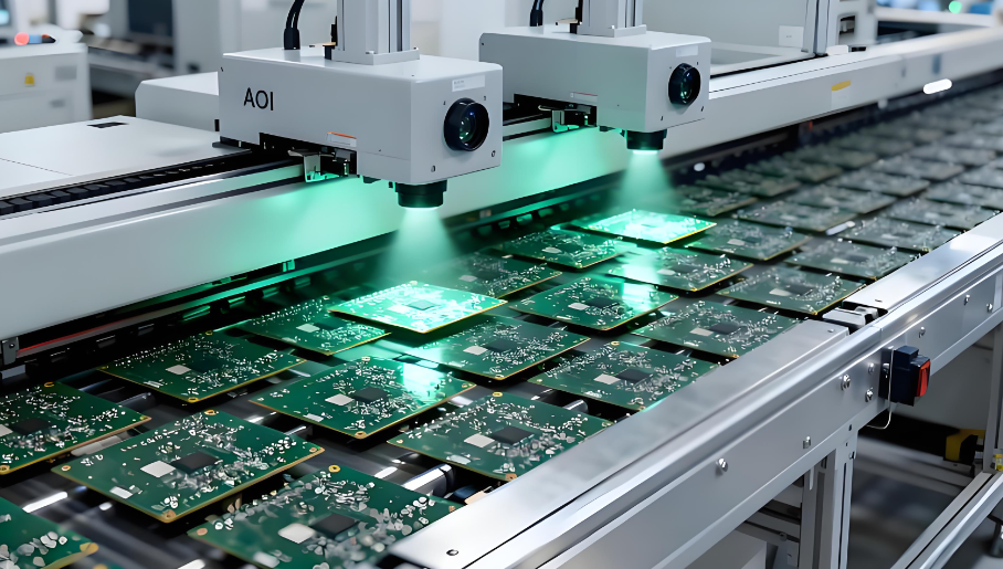
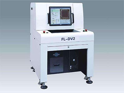
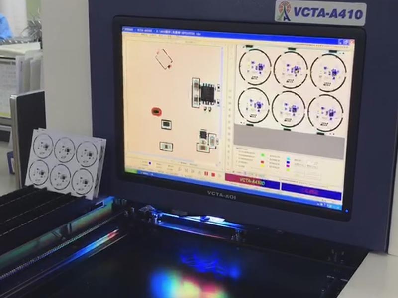
What Is AOI Inspection?
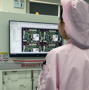
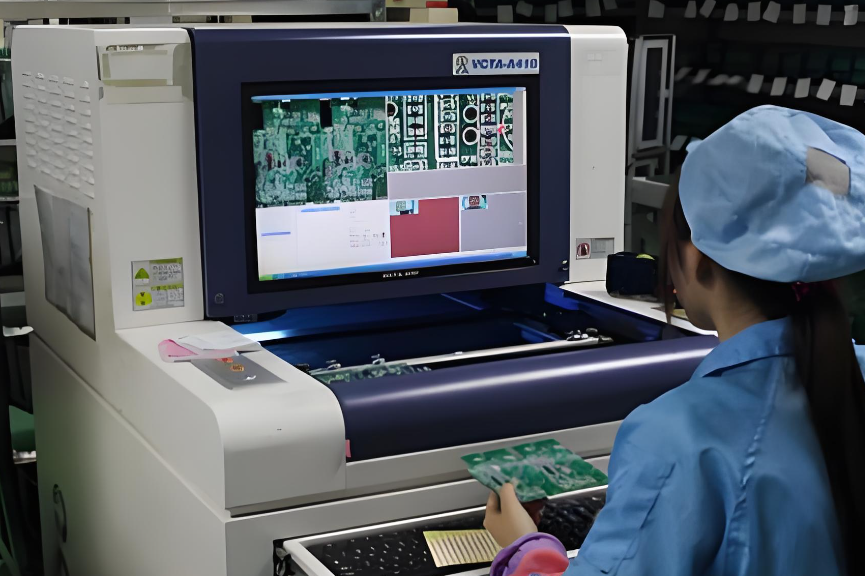
AOI inspection, short for Automated Optical Inspection, is a quality control method used in PCB and PCBA manufacturing to automatically detect visual defects on circuit boards. It relies on high-resolution cameras, controlled lighting systems, and image processing algorithms to evaluate whether a board meets predefined standards.
In modern electronics manufacturing, AOI is not just an optional inspection step. It is a core process that ensures assembly accuracy, especially in high-density SMT production environments where manual inspection becomes inefficient and inconsistent.
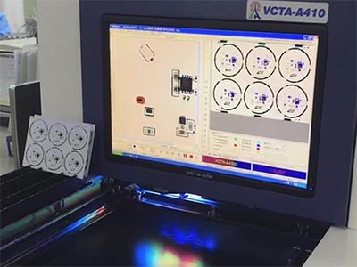
Unlike traditional visual inspection performed by operators, AOI systems provide repeatable and objective results. They compare the inspected PCB against a reference, such as a “golden board” or CAD data, to identify deviations.
How Does AOI Inspection Work in PCB Assembly?
AOI inspection follows a structured process that combines imaging technology with intelligent comparison algorithms.
Step 1: Image Capture
High-speed cameras scan the PCB using multiple light sources. These include white light, RGB, and angled lighting to highlight solder joints and component edges.
Step 2: Reference Matching
The system compares captured images with:
- Golden board samples
- CAD / Gerber data
- Component libraries
Step 3: Defect Detection
Software identifies deviations such as placement errors or solder defects.
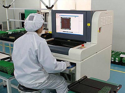
Step 4: Classification & Output
Detected issues are categorized and displayed for operator review or automatically logged into MES systems.
Why Is AOI Inspection Important in SMT Production?
In modern SMT environments, defect tolerance is extremely low due to miniaturization and high-density layouts.
AOI inspection directly improves:
- First Pass Yield (FPY) by detecting issues early
- Process stability through continuous feedback
- Cost control by reducing rework and scrap
- Production efficiency with high-speed inspection
From an engineering standpoint, AOI is not just an inspection tool. It is a process optimization system that helps identify root causes such as stencil wear, placement deviation, or reflow inconsistencies.
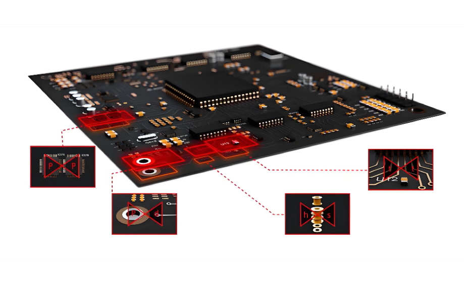
What Defects Can AOI Inspection Detect?
AOI inspection is designed to identify visible defects related to component placement and solder quality. These defects typically include:
- Missing components
- Incorrect components
- Misaligned or shifted components
- Wrong polarity (especially for diodes and ICs)
- Tombstoning (one side lifted)
- Solder bridging
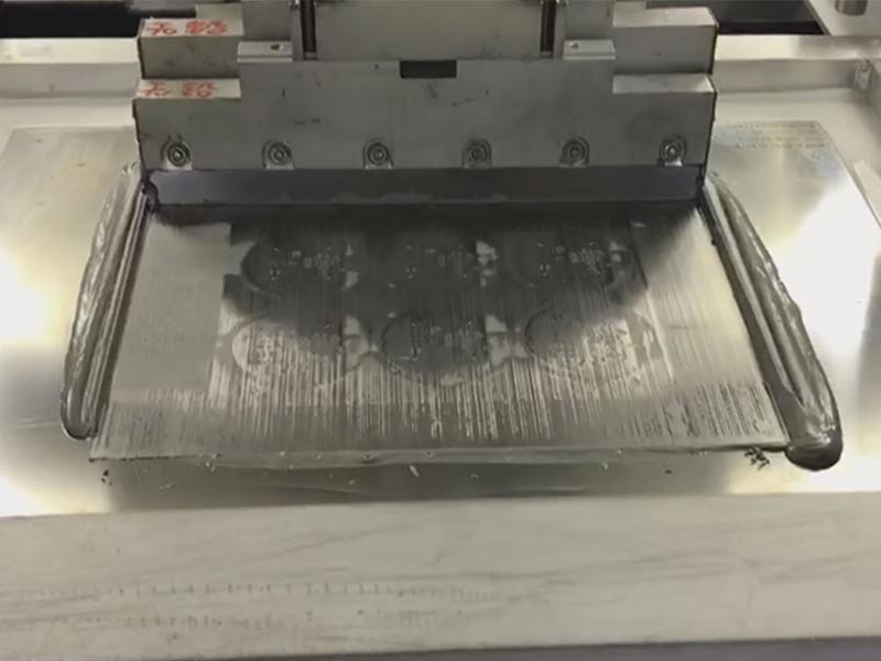
- Insufficient solder
- Excess solder
- Open solder joints
- Lifted leads
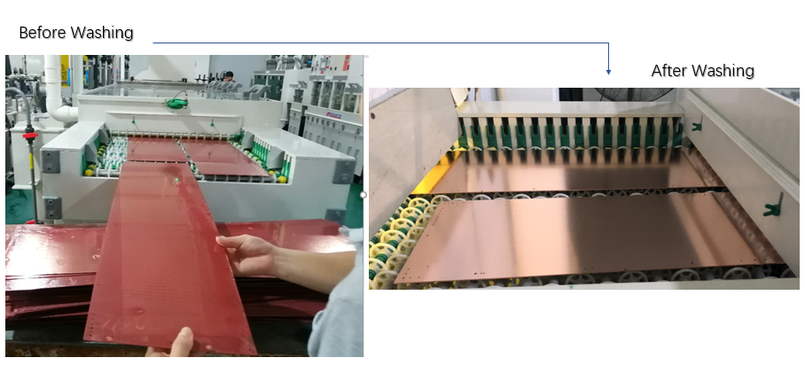
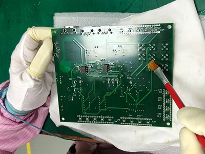
- Surface contamination or scratches
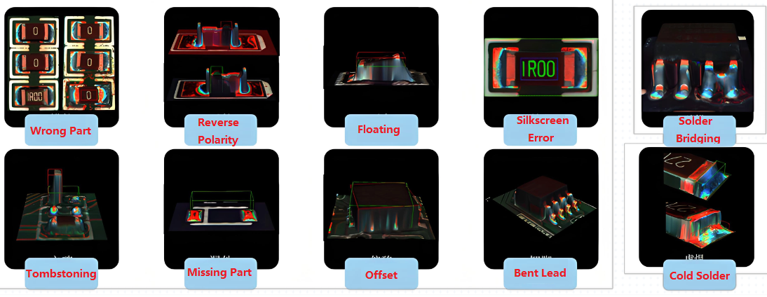
These defects are common in SMT assembly and can significantly affect product performance.
However, AOI focuses on surface-level inspection. It is most effective for defects that can be visually detected. For hidden defects, additional inspection methods are required.
Where Is AOI Inspection Used in the Manufacturing Process?
AOI inspection can be deployed at multiple stages of PCB assembly. Each stage serves a different purpose.
Post-reflow AOI
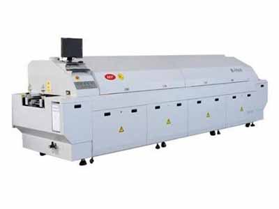
This is the most common AOI stage. It inspects solder joints and component positions after reflow. Most solder-related defects are identified here.
Wave solder AOI
For through-hole components, AOI can be used after wave soldering to inspect solder quality and component insertion.
Final AOI inspection
Some manufacturers include a final AOI step to ensure no defects were missed earlier.
In practice, many high-end SMT lines use multiple AOI checkpoints to maximize defect coverage and process control.
What Are the Main Benefits of AOI Inspection?
AOI inspection delivers measurable benefits across production efficiency and product quality.
- Unlike manual inspection, AOI provides consistent results regardless of operator fatigue or experience.
- AOI systems can inspect thousands of components per second, supporting high-volume production.
- By using AOI inspection, defects are identified immediately, reducing downstream failures.
- Fewer operators are required for inspection tasks
- Inspection data can be analyzed to improve process parameters and prevent recurring issues.
For manufacturers aiming to scale production while maintaining quality, AOI is a fundamental investment.
What Is the Difference Between 2D AOI and 3D AOI Inspection?
AOI systems are typically categorized into 2D and 3D technologies.
| Feature | 2D AOI | 3D AOI |
| Inspection method | Image-based | Height + image analysis |
| Solder evaluation | Limited | Accurate volume measurement |
| Accuracy | Moderate | High |
| Cost | Lower | Higher |
| Application | Standard SMT | High-density / complex boards |
2D AOI relies on color and contrast to detect defects. It is suitable for most standard applications.
3D AOI adds height measurement using techniques such as structured light or laser scanning. This allows it to evaluate solder volume and detect defects that 2D systems may miss.
For advanced applications such as fine-pitch components or reflective surfaces, 3D AOI provides better reliability.
AOI Inspection vs AXI vs Manual Visual Inspection
Different inspection methods serve different purposes in PCB assembly.
AOI vs AXI (Automated X-ray Inspection)
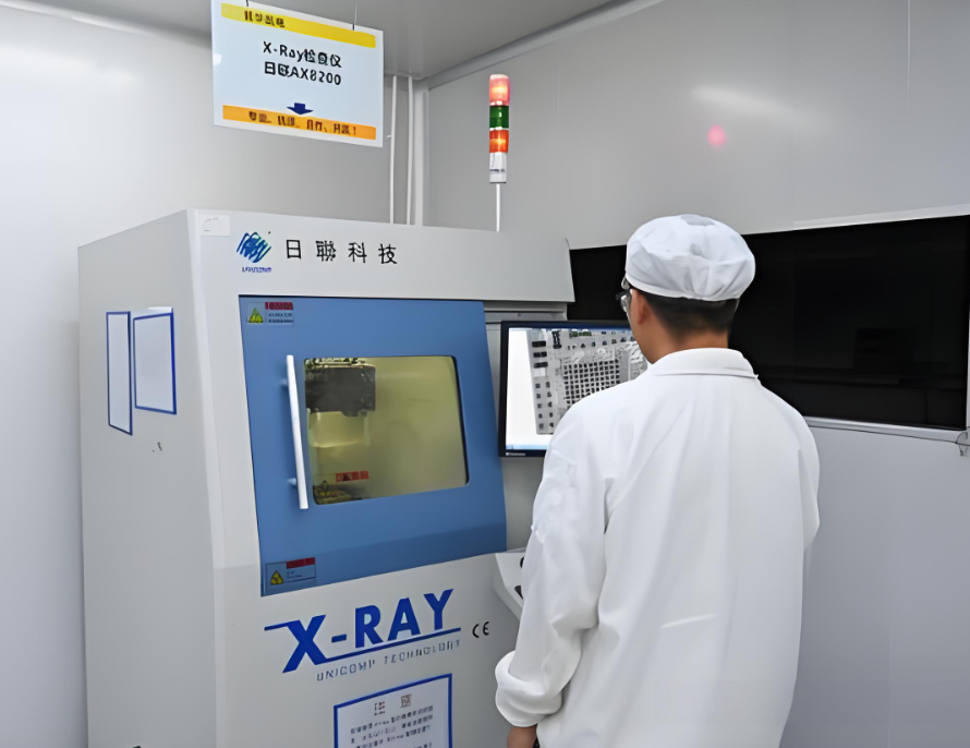
AOI inspects visible surfaces, while AXI is used for hidden structures such as BGA solder joints. AXI can detect voids and internal defects that AOI cannot see.
AOI vs manual inspection
Manual inspection depends on human judgment and is prone to inconsistency. AOI offers higher speed and repeatability.
In practice, these methods are complementary. A typical high-reliability production line may use:
- SPI (Solder Paste Inspection)
- AOI
- X-ray inspection
- Functional testing
This layered approach ensures comprehensive quality control.
What Are the Limitations of AOI Inspection?
While AOI is powerful, it has certain limitations. It cannot effectively inspect hidden solder joints, such as those under BGA components. It also depends heavily on programming quality. Poorly optimized programs can result in false calls or missed defects.
Reflective surfaces and complex geometries can sometimes challenge the system. In addition, AOI requires proper lighting and calibration to maintain accuracy.
Why Choose EBest Circuit (Best Technology) for AOI Inspection and PCBA Quality Control?
At EBest Circuit, AOI inspection is fully integrated into the PCB assembly workflow to ensure consistent quality at every stage.
Key advantages include:
- Advanced AOI systems supporting both prototype and mass production
- Multi-stage inspection strategy (pre-reflow and post-reflow)
- Integration with MES for full traceability
- Experienced engineering team for AOI programming optimization
- Combined inspection capabilities including X-ray, SPI, ICT, and functional testing
- Fast feedback loop to improve yield and reduce defects
With nearly 20 years of PCBA experience, EBest supports industries requiring high reliability, including automotive, medical, and industrial electronics.
FAQs About AOI Inspection
1. What is AOI inspection in PCB assembly?
AOI inspection is an automated method that uses cameras and software to detect visual defects on PCBs. It helps ensure component placement accuracy and solder quality.
2. What is AOI inspection used for?
AOI inspection is used to automatically detect visible defects in PCB assembly, including component placement errors and soldering issues, ensuring product quality and consistency.
3. Can AOI detect all PCB defects?
No, AOI detects only visible defects. Hidden issues such as BGA solder joints require X-ray inspection.
4. Is AOI better than manual inspection?
Yes, AOI is faster, more consistent, and less dependent on human factors, making it more suitable for high-volume production.
5. Where should AOI be placed in SMT lines?
AOI is typically used both before reflow (placement check) and after reflow (solder inspection) for optimal results.
6. What is the difference between 2D and 3D AOI?
2D AOI uses image comparison, while 3D AOI measures height and volume, providing more accurate solder inspection.
Ready to Improve Your PCB Assembly Quality?
If you are facing challenges such as inconsistent quality, high rework rates, or hidden defects in SMT production, integrating AOI inspection is a proven solution.
EBest Circuit offers one-stop PCB and PCBA services, combining advanced AOI inspection with full-process quality control.
Get started today:
- Send your Gerber & BOM for review
- Receive fast DFM + inspection feedback
- Support from prototype to mass production
Contact: sales@bestpcbs.com