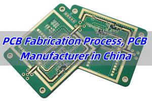
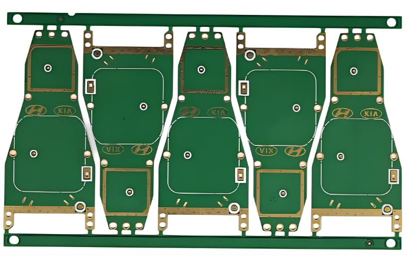
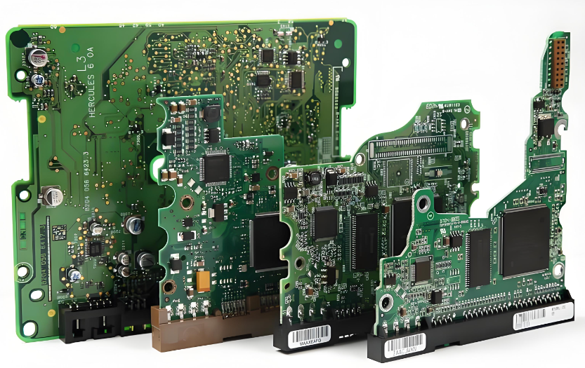
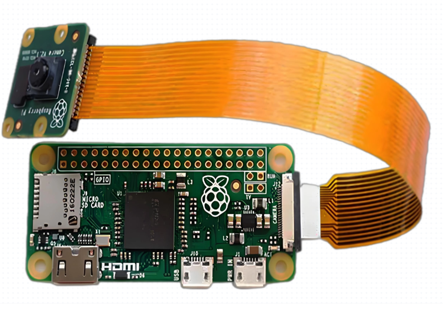
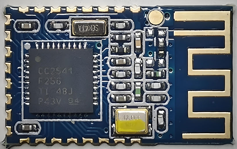
A single sided PCB board has one conductive copper layer on one side of an insulating substrate. It is usually the most economical choice for low-density circuits, provided every trace can be routed without a second copper layer.
This guide explains the board structure, material choices, routing limits, manufacturing sequence, inspection points, applications, and cost drivers. It also shows when a double-sided board is the safer engineering decision.
What Is a Single Sided PCB?
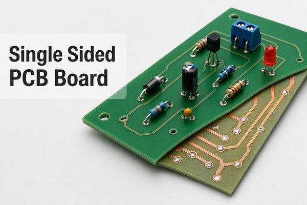
A single-sided PCB uses one patterned copper layer to connect components. The phrase what is single sided pcb usually refers to the same construction as a single-layer PCB: one electrical routing plane, not one physical material layer.
For traditional through-hole assembly, components sit on the non-copper side and their leads pass through holes to solder pads on the copper side. A surface-mount version may place both components and traces on the copper side. Designers choose the assembly style according to component availability, production volume, mechanical demands, and routing space.
How Is a Single Sided PCB Board Constructed?
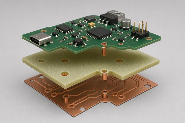
The board combines a rigid base material with one bonded copper foil layer. Solder mask protects the finished conductors, while exposed pads receive a surface finish so they remain solderable.
| Board Element | Common Form | Function |
| Base substrate | FR-4, CEM-1, or CEM-3 | Provides insulation and mechanical support |
| Copper foil | One patterned conductive layer | Forms traces, pads, and electrical connections |
| Solder mask | Applied over the copper side | Protects conductors and controls solder spread |
| Surface finish | HASL, lead-free HASL, OSP, or another specified finish | Protects exposed copper and supports soldering |
| Legend | Reference marks and polarity indicators | Supports assembly and inspection |
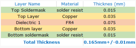
A typical general-purpose board may use 1 oz copper, approximately 35 µm before processing, and a finished thickness around 0.8–1.6 mm. Those are common starting points rather than universal requirements. Current, stiffness, enclosure geometry, depaneling, and component weight can justify other values.
Which Materials Are Used in a Single Sided Copper PCB Board?
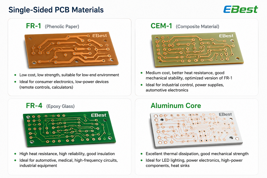
A single sided copper PCB board is commonly made from FR-4 or a composite laminate such as CEM-1 or CEM-3. The right choice depends on electrical performance, temperature exposure, mechanical strength, flame-rating requirements, tooling method, and production volume.
- FR-4: Offers good dimensional stability and mechanical strength for general industrial electronics.
- CEM-1: Often considered for cost-sensitive, high-volume boards with modest mechanical demands.
- CEM-3: Provides a composite construction with properties between paper-based laminates and standard FR-4 options.
- Metal-backed material: Can support thermal management in a single-copper-layer design, but it follows different insulation and machining rules from a conventional FR-4 board.
Copper thickness should match actual current and temperature-rise targets. Use the finished-copper requirement in the fabrication notes and review it with the board supplier; the related guide to PCB copper thickness and tolerance explains why nominal and finished values should not be confused.
What Design Rules Matter for Single Sided PCB Routing?
Single-sided routing succeeds when component placement creates direct paths and keeps conductors from crossing. A layout that needs many jumpers, long detours, or narrow neck-downs has probably exceeded the useful limit of one copper layer.
- Place connectors, switches, and mechanical parts first because their positions are usually fixed.
- Group components by circuit function and keep high-current paths short and wide.
- Reserve enough annular ring around drilled holes for fabrication and soldering variation.
- Avoid routing heat-sensitive signals beside power resistors, regulators, or other hot parts.
- Use jumper wires or zero-ohm resistors only where they simplify the board without creating assembly risk.
- Keep copper away from board edges, slots, mounting hardware, and V-score or routing paths.
- Provide accessible test pads for power rails and important signals.
Do not copy generic trace-width and clearance numbers into a production drawing. The correct values depend on copper thickness, current, voltage, laminate, solder mask, manufacturing class, and the fabricator’s verified capability.
Single Sided PCB Manufacturing Process
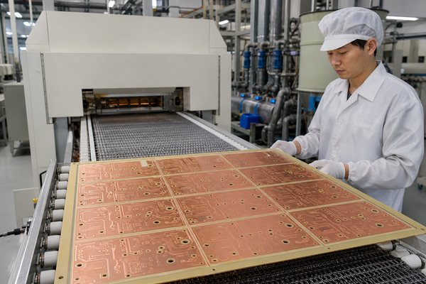
The single sided PCB manufacturing process converts copper-clad laminate into a patterned and protected circuit. It avoids multilayer lamination and interlayer registration, but image quality, etching control, drilling, solder-mask alignment, and final electrical testing still determine whether the board is reliable.
- Material preparation: Cut and clean the selected copper-clad laminate.
- Drilling or punching: Form component holes, tooling holes, and mechanical features.
- Image transfer: Apply the circuit pattern to the copper surface.
- Etching: Remove unwanted copper while preserving specified traces and pads.
- Solder-mask application: Cover conductors while keeping solderable pads exposed.
- Surface finishing: Protect exposed pads with the selected finish.
- Legend printing: Add assembly references, polarity marks, and identification.
- Profiling: Route, punch, or score the finished panel according to the mechanical drawing.
- Electrical test and inspection: Check continuity, isolation, dimensions, hole quality, and visual workmanship.
The existing EBest Circuit overview of single-layer PCB design and prototyping provides additional production context for engineers preparing a new build.
How Are Single Sided PCB Boards Inspected and Tested?
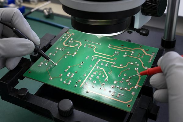
Inspection checks whether the physical board matches the released fabrication data and whether every required electrical connection works. Simple layer count does not remove the need for controlled verification.
- Visual inspection: Finds damaged pads, exposed copper, solder-mask errors, contamination, and rough board edges.
- Dimensional inspection: Confirms outline, hole size, slot location, and critical mechanical features.
- Electrical testing: Detects opens and shorts in the finished copper network.
- Copper and finish checks: Confirm specified conductor build and pad protection when the order requires them.
- Assembly inspection: Reviews solder fill, polarity, component position, and lead trimming after population.
Test access should be designed before layout release. When all critical nodes are reachable from one side, fixtures and troubleshooting remain simpler. If the finished product needs full assembly and functional verification, connect the bare-board plan to the appropriate PCB assembly service requirements.
Difference Between Single Sided PCB and Double Sided PCB
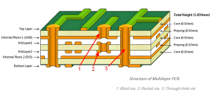
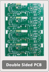
The main difference between single sided PCB and double sided PCB is routing capacity. A double-sided board adds a second copper layer and can connect the two sides through plated holes or vias, which gives the designer more freedom but adds process steps and cost.
| Comparison Point | Single-Sided PCB | Double-Sided PCB |
| Copper layers | One | Two |
| Routing freedom | Limited; traces cannot cross on the same layer | Higher; signals can move between sides |
| Interconnection | No interlayer routing required | Plated through holes or vias connect layers |
| Best fit | Low-density, stable, cost-sensitive circuits | Moderate-density circuits or tighter mechanical envelopes |
| Manufacturing complexity | Lower | Higher due to two-sided imaging and registration |
Choose two layers when jumpers multiply, return paths become poor, EMI control becomes difficult, or the enclosure cannot accept a larger board. A smaller double-sided PCB can be the lower-risk product even when its bare-board price is higher.
Which Applications Fit Single Sided PCBs?
Single-sided boards fit products with low component density, stable electrical requirements, and strong pressure on unit cost. They are especially practical when the circuit will be produced repeatedly and the layout has already been simplified for one-layer routing.
- LED lighting and simple driver boards
- Power adapters and basic power-control modules
- Relays, timers, alarms, and sensor interfaces
- Household appliance control panels
- Chargers, toys, calculators, and consumer accessories
- Simple automotive auxiliary circuits where the approved specification permits the construction
- Educational kits and low-density prototype circuits
Application alone does not decide the layer count. Review current paths, noise sensitivity, connector placement, heat, test access, enclosure size, and expected design changes before locking the structure.
What Are the Main Advantages and Limitations?
The strongest advantage is a short, economical fabrication route. The main limitation is that every connection competes for space on one routing plane.
Advantages
- Lower bare-board cost for suitable designs and production quantities
- Simpler tooling, imaging, inspection, and fault tracing
- Good repeatability for mature low-density products
- Practical for through-hole assembly and straightforward manual repair
Limitations
- Restricted routing density and limited space for continuous ground paths
- More dependence on placement quality and occasional jumper wires
- Larger board area may be needed for the same circuit
- Less flexibility for late component or connector changes
- Not ideal for dense digital circuits, fine-pitch devices, or demanding signal-integrity layouts
What Affects Single Sided PCB Board Price?
Single sided PCB board price depends on more than layer count. Material utilization, order quantity, finished size, copper thickness, hole count, tooling method, surface finish, testing, tolerances, and delivery schedule all affect the quotation.
Large rectangular boards with generous tolerances can be economical, while small boards with many holes, tight routing, unusual outlines, or demanding cosmetics may require more processing than expected. The selected pad finish also matters; for example, a standard lead-free HASL PCB surface finish follows a different process and cost structure from other finish options.
For a meaningful quote, provide Gerber files, a drill file, board thickness, finished copper requirement, solder-mask color, surface finish, outline drawing, panel preference, quantity, test requirement, and delivery target. A PCB prototype manufacturing review can identify missing fabrication notes before the design reaches volume production.
FAQs About Single Sided PCB Boards
Is a single-sided PCB the same as a single-layer PCB?
Yes. Both terms normally describe a PCB with one conductive copper layer. The complete board still contains a substrate, solder mask, surface finish, and possibly a legend, so “single layer” refers to the electrical copper layer rather than every physical coating.
Can SMD components be used on a single-sided PCB?
Yes. Surface-mount components can be placed on the same side as the copper pads. This approach works well when component density remains modest and the assembly process can access all solder joints from that side.
Can a single-sided PCB have plated through holes?
It can, but plated hole barrels do not create a second routing layer by themselves. Many cost-focused through-hole single-sided boards use non-plated component holes and form solder joints on the copper side. The drawing must state the required hole treatment clearly.
What copper thickness is common for a single-sided board?
One-ounce copper, approximately 35 µm before processing, is a common starting point for general electronics. Higher or lower copper may be appropriate. Confirm the finished thickness and current-carrying requirement with the fabricator rather than treating 1 oz as a universal rule.
Why do some single-sided PCBs use jumper wires?
A jumper crosses another conductor without adding a second copper layer. A few jumpers can keep a simple board economical. Many jumpers increase assembly work and error opportunities, which can make a double-sided layout more practical.
Can a single-sided PCB carry high current?
Yes, if conductor width, copper thickness, temperature rise, terminal design, and heat dissipation are engineered for the load. High current alone does not require two layers, but narrow space or poor thermal paths may make another construction safer.
Which surface finishes can be used?
Common options include HASL, lead-free HASL, and OSP, with other finishes available when the pad geometry, storage requirement, assembly method, or product specification justifies them. Select the finish according to the actual soldering and reliability requirements.
When should a design move to a double-sided PCB?
Move to two layers when routing requires many jumpers, the board becomes too large, return paths are weak, sensitive signals cannot be separated, or future changes are likely. Compare total product and assembly risk, not only the bare-board price.
Are single-sided PCBs suitable for prototypes?
Yes. They work well for low-density prototypes and make manual probing easy. A prototype may still use two layers if layout changes are expected or if the final product needs a smaller, cleaner, or more noise-resistant routing structure.
What files are needed to manufacture a single-sided PCB?
Provide Gerber data for the copper, solder mask, and legend; an NC drill file; a clear outline; and fabrication notes covering material, thickness, copper, finish, color, quantity, and testing. Assembly projects also need BOM and component-placement data.
How Can EBest Circuit Support a Single Sided PCB Project?
At EBest Circuit, we have provided PCB and PCBA services since 2006. We support PCB design, prototyping, mass production, component sourcing, and assembly, allowing engineering and procurement teams to coordinate bare-board fabrication and assembly within one project.
For a single-sided PCB project, our engineers can review the material, finished copper, surface finish, routing, manufacturability, testing, and assembly requirements. The review can also identify when a one-layer design remains practical and when a double-sided layout may reduce routing or production risk.
To request an engineering review and quotation, send your Gerber files, NC drill data, board specifications, quantity, and delivery target to sales@bestpcbs.com. Include the BOM and component-placement files when assembly is required, so we can evaluate the complete single sided PCB board project.