





Learning how to desolder a circuit board starts with choosing a removal method that suits the component. Through-hole parts usually need solder extraction from plated holes, while surface-mount parts need all their solder connections released before lifting. In both cases, controlled heat, suitable flux, and minimal mechanical force help preserve the copper pads and traces.
Start with a simple component on a practice board. Secure the PCB, identify every soldered connection, and check that the part moves freely before removing it. For dense assemblies, hidden-pad packages, or valuable boards, the right rework equipment and inspection plan become especially important.
What Tools Do You Need to Desolder a Circuit Board?
A temperature-controlled soldering station, suitable solder-removal tool, compatible flux, board holder, and magnification form a practical starting kit. Choose the tip and extraction method around the joint size and board construction.
A very fine tip is not always the best choice. A connector mounting tab or ground-connected pin can draw heat away quickly. A suitably sized chisel tip often transfers heat more effectively than a needle tip, helping the solder melt without prolonged contact.
| Tool | Main use | What to check |
|---|---|---|
| Temperature-controlled soldering station | Heating accessible solder joints | Tip size, tip condition, and thermal recovery |
| Manual desoldering pump | Extracting molten solder from accessible through-hole joints | Nozzle condition, access, and suction |
| Powered desoldering tool | Clearing multiple through-hole pins | Nozzle fit, vacuum path, filters, and maintenance |
| Solder wick | Removing bridges and residual solder from pads | Braid width, flux compatibility, and condition |
| Hot-air rework station | Heating multiple surface-mount connections together | Nozzle, airflow, component limits, and thermal profile |
| Heated tweezers | Removing suitable two-terminal SMD parts | Tip alignment and contact with both terminations |
| PCB holder and magnification | Supporting the assembly and inspecting connections | Stable support and access to both board sides |
| Fume extraction and eye protection | Managing fumes and solder splashes | Extraction position and clear visibility |
Keep a heat-resistant tool stand nearby. For static-sensitive electronics, use an appropriate ESD-controlled workstation.
Cleaning materials also belong in the kit, but select them for the flux and assembly. A solvent suitable for one board may affect another board’s coating, markings, adhesives, or plastic parts.
What Should You Check Before Heating the PCB?
Disconnect power, remove accessible batteries, and confirm that stored electrical energy has been safely discharged before handling the assembly. Power supplies, flash circuits, motor drives, and similar equipment can retain hazardous energy after unplugging. These assemblies require qualified handling.
Next, photograph the component and surrounding area. Record polarity, pin 1, connector orientation, and any existing damage. A clear image makes replacement and later inspection easier.
Check the following before choosing a technique:
- Package and connections: Identify through-hole leads, surface-mount terminals, exposed pads, shield tabs, and mechanical anchors.
- Board construction: Look for multilayer copper, large ground areas, metal substrates, or other features that increase heat demand.
- Nearby materials: Locate plastic connectors, cables, batteries, adhesives, coatings, and heat-sensitive components.
- Removal purpose: Decide whether the component must survive or whether preserving the PCB takes priority.
- Available documentation: Review the component drawing, assembly information, and applicable rework instructions.
Some parts have adhesive beneath their bodies or solder connections hidden from view. A component that remains attached after visible joints are released may still have another attachment point.
Confirm the complete attachment before applying lifting force. This is especially important with shielded connectors, QFN devices, and packages with exposed thermal pads.
What Temperature Should You Use for Desoldering?
Choose the tool setting according to the solder alloy, joint size, thermal mass, equipment, and component limits. A single temperature range cannot describe every board, and a fixed contact time cannot guarantee pad protection.
The station display shows a tool setting. It does not directly tell you the temperature inside a plated hole or beneath a component. A small tip touching a heavy ground joint may transfer heat poorly even when its displayed temperature is high.
For hot-air rework, measure the thermal profile at the component and relevant solder joints. The nozzle setting is not the joint temperature. Check the package rework limits before selecting preheat, airflow, peak temperature, and heating duration.
For accessible hand-tool work, assess heat transfer in this order:
- Check the tip surface. It should accept solder and make effective contact.
- Match the tip to the joint. Use enough contact area to transfer heat without touching neighboring features.
- Apply compatible flux. This helps remove oxides and supports wetting.
- Observe solder flow. The joint must be molten where separation or extraction needs to occur.
- Reassess unsuccessful attempts. Change the setup instead of repeating long heating cycles.
Flux helps solder wet clean metal surfaces. Ordinary flux does not lower the solder alloy’s melting point. Low-melting removal alloys are separate products with their own compatibility and cleanup requirements.
If a joint repeatedly resists melting, investigate the copper mass, tool performance, solder condition, and need for controlled preheating.
Which tip temperatures suit each removal method?
For heated-nozzle vacuum removal, a small-joint starting range is 320–360°C, while larger joints may need 370–400°C. For compatible high-temperature, no-clean lead-free braid, the iron range is 650–750°F, approximately 343–399°C, at the iron. Select the range for the removal method and verify heat transfer on the actual joint.
| Removal process | Tip / iron temperature | Heating or release check |
|---|---|---|
| Small accessible joint; heated vacuum nozzle | 320–360°C (608–680°F) | Check for release after about 2–3 s with a suitable heated nozzle; confirm molten solder and a free lead before suction. |
| Larger joint; heated vacuum nozzle | 370–400°C (698–752°F) | No universal dwell time. Verify melting through the connection; reassess heat transfer if release fails. |
| Exposed-pad cleanup with compatible lead-free no-clean braid | Approx. 343–399°C (650–750°F) | Remove braid and iron together when solder uptake stops, while the joint is still molten. |
Use these temperatures only with equipment, consumables, and joint conditions that support the relevant process. The vacuum examples do not establish a universal leaded-versus-lead-free setting, and the braid range does not apply to every flux system. None is a hot-air nozzle setting or a measured solder-joint temperature.
How many seconds should the tip contact the joint?
With a suitable heated vacuum nozzle, check the lead for release after about 2–3 seconds of heating. This is a process-specific inspection interval, not a guaranteed maximum safe contact time. Validate the temperature and release-check interval together for the actual tool, joint and assembly before routine use.
If the lead remains held, do not pull it or repeat identical heating cycles. Remove the tool and reassess nozzle contact, copper mass, flux, and extraction performance. Follow the assembly’s thermal limits before another attempt. Wick cleanup and hot-air removal need their own release criteria; a 2–3 second nozzle check cannot be transferred to a QFN, BGA, or connector heating cycle.
What are the melting temperatures of common solder alloys?
Solidus marks the beginning of melting; liquidus marks complete melting. Use the liquidus to interpret joint release, not as an iron setpoint.
| Solder alloy | Solidus (°C) | Liquidus (°C) |
|---|---|---|
| Sn63Pb37 | 183 | 183 |
| Sn60Pb40 | 183 | 190 |
| SAC305 / Sn96.5Ag3Cu0.5 | 217 | 220 |
| Sn99.3Cu0.7 | 227 | 227 |
For example, Sn60Pb40 can be partly molten between 183°C and 190°C. A SAC305 joint needs to pass its approximately 220°C liquidus to become fully molten, but this does not justify setting a hot-air station to 220°C and assuming the hidden joints reach that temperature. Mixed or unknown alloys require separate assessment.
How Do You Desolder Through-Hole Components?
Through-hole removal requires releasing each lead from the solder inside its plated hole. A clean-looking surface alone does not prove that the lead is free.
For a simple resistor or similar accessible component, a soldering iron and manual pump may be sufficient. Multi-pin headers and connections to heavy copper often benefit from a powered desoldering tool.
Follow this sequence:
- Support the PCB. Position the target joints for comfortable access while keeping the board stable.
- Apply compatible flux. Place it at the joint rather than coating unrelated areas.
- Prepare the extraction tool. Prime a manual pump or check the powered tool’s nozzle and vacuum path.
- Heat the connection. Bring the solder around the lead into a molten state before extraction.
- Remove the molten solder. Position the nozzle close enough to collect it effectively.
- Inspect the lead and hole. Check for solder remaining around the lead or on the opposite board side.
- Repeat only where needed. Correct poor heat transfer or extraction before another attempt.
- Lift the released component. Use minimal force once every lead and attachment is free.
Before applying vacuum, confirm that solder has melted through the connection, not just on the visible surface. Internal copper planes can draw heat away from the plated hole even when the surface solder appears liquid.
A small amount of fresh, compatible solder can sometimes improve thermal contact with an oxidized or partly emptied joint. Confirm alloy compatibility when the assembly has controlled material requirements.
Keep drills and sharp probes out of plated holes during routine solder removal. Mechanical scraping can damage the copper barrel. Restore solder flow and use an appropriate extraction method instead.
How Do You Use Solder Wick Without Lifting Pads?
Solder wick draws molten solder into copper braid by capillary action. It works well for bridges and accessible residual solder, particularly when preparing surface pads after removal.
Choose a braid width suited to the pad or solder area. Excessively wide braid adds thermal mass and can heat neighboring features. Saturated braid has limited capacity, so advance to a fresh section as needed.
Use this sequence:
- Place a fresh section of suitable braid over the solder.
- Apply the soldering tip to the braid so heat reaches the joint beneath it.
- Allow the molten solder to enter the braid with light contact.
- Remove the iron and braid together while the solder remains molten.
- Inspect the pad before making another pass.
Lift the braid and iron together while the solder is molten. If the braid sticks, reheat the connection before lifting; do not pull cold braid away from the pad.
Let heat and capillary action do the work. Heavy pressure, scrubbing, and pulling cold braid place unnecessary stress on the copper.
The goal is a usable pad surface for the next assembly step. Repeatedly chasing a perfectly bare copper appearance adds heat exposure without necessarily improving the repair.
Which braid width fits the solder area?
Choose braid approximately as wide as, or slightly wider than, the exposed connection without touching adjacent features. Common nominal braid widths include:
| Nominal braid width | Approx. inch size |
|---|---|
| 1.5 mm | 0.060 in |
| 2.0 mm | 0.080 in |
| 2.8 mm | 0.110 in |
These are braid dimensions, not required pad widths. Match the tip contact area to the braid and joint. Move to a fresh section once the braid fills instead of adding pressure or extending contact to compensate.
How Do You Desolder SMD Components With a Soldering Iron?
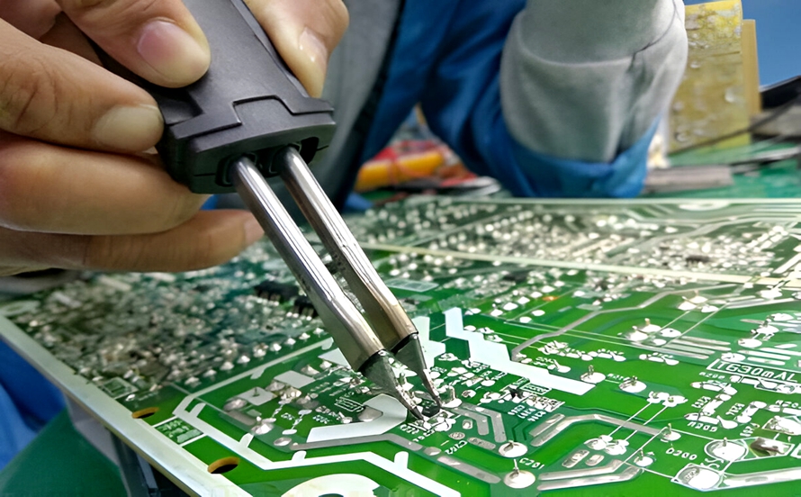
Small two-terminal SMD components can be removed with suitable hand tools when both solder joints can remain molten during removal. Heated tweezers provide a useful option because they heat both terminations together.
The important point is the condition of both connections at the moment the part moves. Lifting one end while the other end remains soldered transfers force into the remaining pad and component termination.
For suitable two-terminal parts:
- Apply compatible flux to both terminations.
- Choose tips that make controlled contact with the joints.
- Heat both connections using heated tweezers or another suitable simultaneous-heating method.
- Lift the component gently once it is fully released.
- Prepare and inspect the pads after removal.
A single iron may suit some accessible packages and operator techniques. If both joints cannot be kept molten reliably, change the removal method.
For three-terminal devices and larger packages, inspect the footprint carefully. Some devices include a large soldered tab beneath or beside the body. Heating only the small visible leads leaves that connection attached.
Practice on a scrap board before working on a valuable assembly. Larger, accessible components make it easier to observe solder flow and learn how little force a fully released part requires.
How Do You Remove ICs and Hidden-Pad Components?
Select the removal process around the package connections. SOIC and QFP devices have visible perimeter leads, while QFN and BGA packages include solder joints beneath the body.
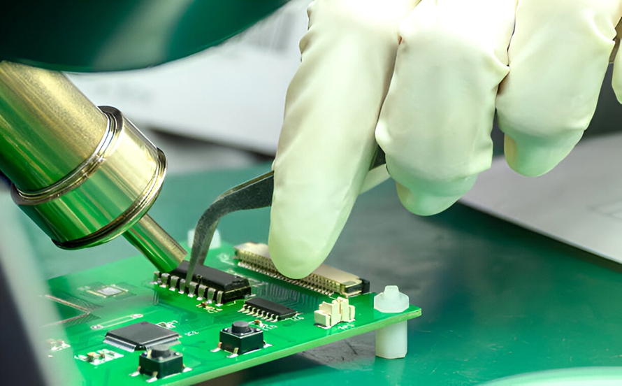
For visible-lead ICs, suitable hot-air equipment can heat the connections together. Some specialist removal methods use a compatible low-melting alloy, followed by thorough removal of that alloy before replacement.
Removing solder from visible leads does not prove that the entire package is released. An exposed thermal pad, concealed joint, adhesive, or underfill may still hold it in place.
A controlled IC removal process should address:
- Package identification and orientation.
- Moisture sensitivity and handling requirements.
- Nozzle size and access around the component.
- Board support and any required underside heating.
- Temperature measurement at relevant locations.
- Protection of nearby parts.
- A lifting method that applies minimal force after release.
Hidden-joint packages require a process that heats the underside connections sufficiently while respecting the limits of the package and surrounding assembly.
Stop if the component resists lifting. Recheck the attachment and heating process before continuing. Increasing force can turn a replaceable component problem into damaged pads or broken internal connections.
For dense, underfilled, or high-value assemblies, professional rework offers better control over removal, replacement, and verification.
How Do You Desolder an HDMI Port or Large Connector?
An HDMI port can combine fine signal contacts, large shield anchors, plastic insulation, and connections to substantial ground copper. The exact construction varies, so inspect the connector drawing and both sides of the board first.
Signal pins and mechanical anchors need separate attention. Fine contacts may release while the shield tabs remain firmly attached, or the reverse.
A practical removal plan is:
- Identify every attachment. Locate signal contacts, shield tabs, locating features, and any adhesive.
- Inspect surrounding parts. Check nearby plastic components, small passives, and cables.
- Choose the heating approach. Consider the connector’s thermal mass and whether controlled preheating is required.
- Release the connections. Use equipment suited to the fine contacts and larger anchors.
- Confirm full release. Lift only when every attachment permits removal with minimal force.
- Inspect the footprint. Check signal pads, anchor holes, traces, and nearby components.
Avoid levering the connector against the PCB. A loose-looking housing may still be attached by one contact or a concealed shield connection.
After removal, evaluate any damaged signal path before choosing a repair. HDMI uses high-speed differential connections, so a jumper that restores DC continuity may still alter signal behavior. Repair planning must consider geometry, electrical performance, mechanical strength, and access for inspection.
What Common Mistakes Cause Desoldering Damage?
The most consequential mistakes involve moving a component before release, repeating ineffective heating, or overlooking part of the attachment.
- Pulling while one joint remains solid: Transfers removal force into pads and traces. Confirm every connection is released.
- Choosing a tiny tip for heavy copper: Limits heat transfer and encourages long contact. Match tip area and tool capacity to the joint.
- Repeating unsuccessful heating cycles: Adds cumulative thermal exposure. Reassess the tool, contact, extraction, and board mass.
- Pulling braid after it cools: Can pull copper away with the braid. Reheat and release it while molten.
- Clearing holes with a drill: Can cut or remove plated copper. Use controlled heating and solder extraction.
- Tapping the PCB to throw off solder: Scatters hot metal and stresses the assembly. Collect solder with a suitable removal tool.
- Ignoring shield tabs or thermal pads: Leaves the component mechanically attached. Inspect the complete footprint.
- Cleaning every flux with the same solvent: May leave residue or affect assembly materials. Follow the flux and material compatibility guidance.
Another common error is treating the highest available temperature as the quickest solution. Effective heat transfer comes from the whole setup: tool capacity, tip contact, joint condition, and board construction.
Stop and reassess when the process stops working. A change in equipment or technique is usually more useful than another identical heating attempt.
How Should You Inspect and Test the Board After Desoldering?
Allow the assembly to cool sufficiently for handling, then inspect the removal area under magnification. Compare it with the photographs taken before work.
Check both sides of the board where accessible:
- Pads: Look for lifting, peeling, missing copper, or movement.
- Traces: Inspect for scratches, breaks, and separation near pad edges.
- Plated holes: Check for obstruction and visible barrel damage.
- Laminate: Look for blistering, charring, or separation.
- Adjacent parts: Check alignment, cracked bodies, disturbed joints, and heat effects.
- Residue and debris: Locate solder balls, bridges, braid fragments, and cleaning residue.
Clean according to the flux manufacturer’s guidance and the assembly’s compatibility requirements. Isopropyl alcohol suits some residues, while other materials require a different process. Keep solvent away from ignition sources and allow the assembly to dry fully.
Before power-up, perform relevant electrical checks. These may include continuity along the affected net, checks for unintended connections between neighboring pads, and comparison of power-rail resistance with expected behavior. Low resistance alone does not establish a fault on every circuit.
Inspection after removal and verification after replacement are separate steps. Once the replacement is fitted, confirm orientation, solder-joint condition, and suitable functional performance. Hidden-joint packages may require additional inspection methods.
For production assemblies, record the board revision, component location, work performed, inspection result, and test outcome. This creates a useful reference if the same issue appears again.
When Should You Use Professional PCB Rework?
Professional rework is appropriate when successful removal depends on controlled thermal profiling, hidden-joint inspection, specialized pad repair, or verification beyond basic bench testing.
Consider it for BGA and QFN packages, fine-pitch connectors, multilayer boards with heavy copper, moisture-sensitive components, underfilled devices, and assemblies with existing pad or barrel damage.
The decision also depends on board value and application. A practice board offers room to learn. A medical, automotive, or other reliability-sensitive assembly needs a documented process and acceptance criteria suited to its use.
Where pad repair is permitted, evaluate the original connection, required current, mechanical loading, spacing, and signal function before selecting a repair method. A successful continuity reading alone does not establish that the repair is suitable for service.
If a PCB assembly project involves component replacement, assembly defects, or recurring soldering problems, contact EBest Circuit at sales@bestpcbs.com. Send clear photographs, the board revision, component reference and part number, quantities, and fault details so our engineering team can review the project requirements and available support.
FAQ About Circuit Board Desoldering
Q1: Does old solder have a higher melting point than fresh solder?
A1: Age alone does not define an alloy’s melting point, although oxidation and joint condition can make effective heating and wetting more difficult.
Q2: Can I mix leaded and lead-free solder during removal?
A2: Mixing alloys changes the joint composition, so use a method compatible with the assembly’s material, compliance, and reliability requirements.
Q3: Should I cut a faulty component’s leads before removing it?
A3: Cutting accessible leads can simplify removal when the component is being discarded, provided the cutting action places no damaging load on the PCB.
Q4: Can conformal coating stay in place during desoldering?
A4: Coating around the work area generally requires controlled local removal using a method suited to its chemistry and the underlying assembly.
Q5: Can a removed component be reused?
A5: Reuse depends on the component’s condition, thermal history, handling requirements, and the acceptance rules for the application.
Q6: Should a PCB be baked before rework?
A6: Baking depends on moisture exposure, component requirements, and the permitted temperature limits of the complete assembly.
Q7: Does solder wick expire?
A7: Solder wick has product-specific storage and shelf-life requirements because oxidation and flux condition affect its performance.
You may also like



Tags: How to Desolder, How to Desolder a Circuit Board, How to Desolder Circuit Board Components