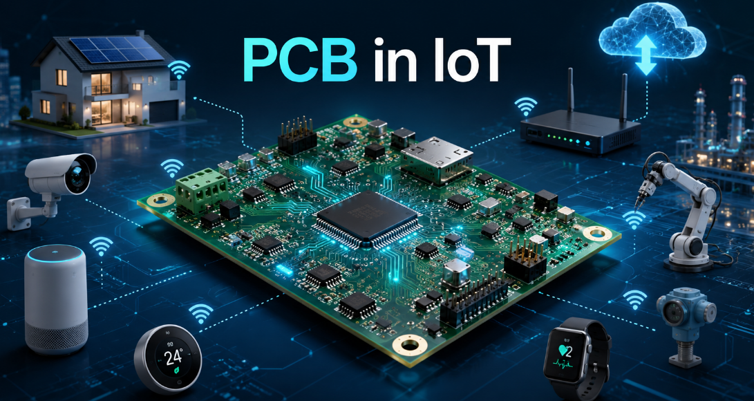
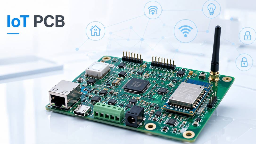
What is PCB in IoT, and why does it matter for reliable smart devices? In every connected product, the PCB supports sensors, wireless modules, power circuits, connectors, and control components, making it the hardware foundation of IoT performance.
A well-designed PCB in IoT can improve wireless stability, battery life, signal accuracy, assembly yield, and long-term reliability. For smart sensors, gateways, trackers, wearables, access control systems, and industrial IoT devices, choosing the right PCB design, manufacturing, and assembly process helps reduce project risk before mass production.
What is PCB in IoT?
PCB in IoT refers to the printed circuit board used inside Internet of Things devices. It connects sensors, microcontrollers, wireless modules, power circuits, connectors, antennas, and protection components.
In an IoT product, the PCB works as the hardware foundation. Sensors collect data, the microcontroller processes signals, the wireless module sends or receives information, and the power circuit supplies stable voltage. All these functions depend on the PCB.
Common IoT devices that use PCB include:
- Smart sensors
- Wearable devices
- Smart meters
- GPS trackers
- Wireless access control systems
- Industrial monitoring devices
- Smart home devices
- Medical monitoring equipment
A good PCB for IoT should support compact size, stable wireless communication, low power consumption, and reliable long-term operation.
What is PCB in IoT Full Form?
The full form of PCB in IoT is Printed Circuit Board in Internet of Things. PCB means Printed Circuit Board. IoT means Internet of Things. So, PCB in IoT means the circuit board used in smart connected devices that collect, process, transmit, or receive data.
For example, a smart temperature sensor may include:
- Temperature sensor
- Bluetooth, Wi-Fi, LoRa, NB-IoT, or LTE module
- Microcontroller
- Battery management circuit
- Antenna area
- Programming port
- Protection components
The PCB is the physical base of the IoT hardware. Software, cloud platforms, and mobile apps are important, but the actual sensing, communication, and power control functions start from the PCB.
Why is PCB Important for IoT Devices?
PCB is important for IoT devices because it directly affects performance, reliability, size, power efficiency, and production quality.
For wireless IoT products, PCB layout affects antenna performance, RF signal strength, communication distance, and data stability. Poor layout may cause weak wireless signals even when the wireless module itself is good.
For battery-powered IoT devices, PCB design affects battery life. Low-power components, efficient voltage regulation, and clean power routing help reduce energy loss.
For mass production, PCB quality also affects assembly yield. Proper pad design, solder mask clearance, test points, and component spacing help reduce soldering defects and rework.
A reliable PCB in IoT helps improve:
- Wireless signal stability
- Battery life
- Device miniaturization
- Sensor accuracy
- Assembly reliability
- Long-term operation
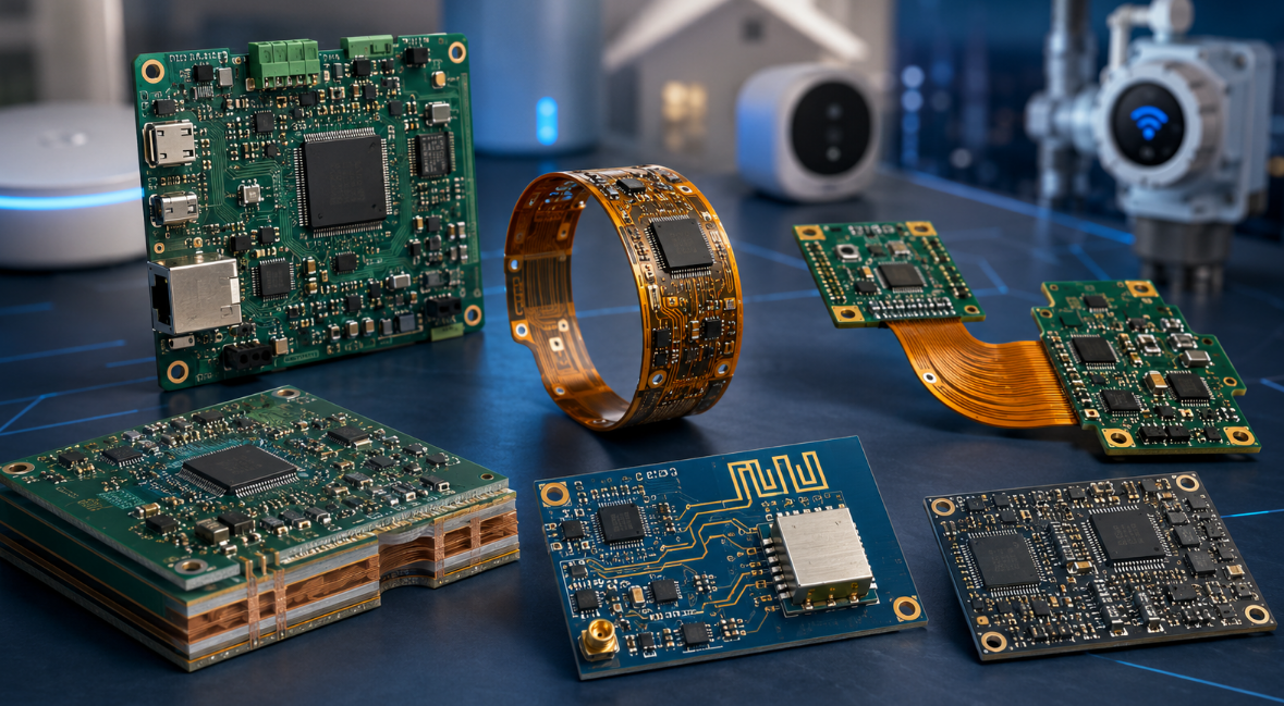
What Types of PCB Are Used in IoT Products?
Different IoT products use different PCB types based on size, wireless function, power design, and application environment. The right PCB structure can improve signal stability, assembly quality, and product reliability.
- Rigid PCB
Rigid PCB is the most common choice for IoT products such as smart sensors, gateways, smart meters, and access control devices. It has stable structure, mature production, and good cost control. - Flexible PCB
Flexible PCB is suitable for wearable devices, medical sensors, compact trackers, and products with curved or limited space. It helps save space and fit special product shapes. - Rigid-flex PCB
Rigid-flex PCB combines rigid and flexible sections. It is used in compact IoT devices that need fewer connectors and higher reliability. It can reduce connection failure and improve vibration resistance. - Multilayer PCB
Multilayer PCB is used in IoT products with wireless modules, sensors, processors, and multiple interfaces. It improves grounding, EMI control, power distribution, and signal integrity. - High-frequency PCB
High-frequency PCB is used for RF and wireless IoT products, such as GPS, GNSS, UWB, LoRa, LTE, and NB-IoT devices. It supports stable high-frequency signal transmission. - HDI PCB
HDI PCB is used for miniaturized IoT devices with dense routing and fine-pitch components. It allows more circuits in a smaller board size.
In most IoT projects, rigid PCB and multilayer PCB are commonly used. For smaller or more advanced products, flexible PCB, rigid-flex PCB, high-frequency PCB, or HDI PCB may be required.
What Should Be Considered When Designing PCB in IoT?
Designing PCB in IoT should focus on wireless performance, power consumption, board size, signal stability, assembly, and testing. IoT devices are often small, wireless, and battery-powered, so PCB design must match the real product application.
- Confirm product requirements first
Confirm the device function, communication method, power source, enclosure size, working environment, and testing needs before starting the PCB layout. - Plan the wireless area early
For Wi-Fi, Bluetooth, Zigbee, LoRa, LTE, NB-IoT, GPS, GNSS, UWB, or NFC devices, plan the antenna position, RF trace, ground area, and keep-out zone before component placement. - Protect the antenna keep-out area
Keep copper, batteries, metal parts, large connectors, and tall components away from the antenna area. Poor antenna clearance can reduce signal strength and communication distance. - Choose the right PCB layer structure
Simple IoT devices may use 2-layer PCB. Products with RF circuits, dense components, or better EMI control often require 4-layer or 6-layer PCB. - Separate RF, power, and digital circuits
Keep switching power circuits, clock signals, and high-speed digital lines away from RF traces and antenna areas. This helps reduce noise and improve wireless stability. - Design for low power consumption
Battery-powered IoT devices should use low-current components, efficient power circuits, sleep mode support, and clean power routing. - Place sensors correctly
Keep temperature sensors away from heat sources. Place environmental sensors where airflow is available. Poor sensor placement can cause inaccurate data. - Reserve test points
Add test points for power rails, programming, communication interfaces, reset pins, and key signals. This makes debugging, firmware programming, and production testing easier. - Match the final enclosure
Check PCB size, connector position, antenna direction, battery location, mounting holes, and component height. The PCB should fit the enclosure without blocking wireless signals. - Design for SMT assembly
Use proper pad size, component spacing, polarity marks, solder mask clearance, and panelization. Good assembly design helps reduce soldering defects and rework. - Check heat and protection needs
Power parts, charging ICs, and wireless modules may generate heat. Outdoor or industrial IoT devices may also need ESD, surge, humidity, and vibration protection. - Review DFM before production
Check Gerber files, BOM, pick-and-place files, stack-up, impedance requirements, test points, and assembly drawings before manufacturing.
A good PCB in IoT should support stable wireless communication, long battery life, accurate sensing, smooth assembly, easy testing, and reliable field operation.
How Does PCB Layout Affect Wireless Performance in IoT Devices?
PCB layout has a direct impact on wireless performance in IoT devices. Even if the wireless module is high quality, poor PCB layout can still cause weak signal, short communication distance, unstable connection, high noise, and failed RF testing.
- Antenna placement affects signal strength
The antenna should be placed at the board edge or in an open area whenever possible. It should not be surrounded by copper, batteries, metal parts, large connectors, or tall components. Poor antenna placement can reduce wireless range and make the signal unstable. - Antenna keep-out area must be protected
Most wireless modules have a recommended antenna keep-out area. This area should remain free of copper, ground planes, components, screws, metal shells, and cables. If this area is not protected, Wi-Fi, Bluetooth, LoRa, NB-IoT, GPS, GNSS, UWB, or Zigbee performance may be affected. - RF trace routing should be short and controlled
RF traces should be as short and direct as possible. Long or poorly routed RF traces can create signal loss and impedance mismatch. For many RF designs, 50-ohm controlled impedance is commonly required. - Ground design affects RF stability
A stable ground plane helps reduce noise and improve signal return paths. Poor grounding can cause interference, unstable communication, and lower RF efficiency. Via stitching around RF areas can also help improve shielding and signal stability. - Power noise can interfere with wireless signals
Switching power circuits, clock lines, and high-speed digital traces should be kept away from RF traces and antenna areas. Noise from these circuits may reduce receiver sensitivity and cause unstable wireless connection. - Component placement should avoid RF interference
Crystals, DC-DC converters, processors, displays, motors, and cables may generate interference. These parts should not be placed too close to the antenna or RF path. Proper spacing helps reduce EMI problems. - Matching components should be placed near the antenna
RF matching components should be placed close to the antenna feed point. This allows tuning during testing and helps improve signal transmission. Poor placement of matching components may make RF optimization difficult. - The enclosure can change wireless performance
The PCB may work well during bench testing but fail after installation in the final housing. Plastic thickness, metal parts, battery position, screws, and installation direction can all affect antenna performance. - Final product RF testing is necessary
Wireless performance should be tested after the PCB is assembled into the final enclosure. Testing should include signal strength, communication distance, connection stability, current consumption during transmission, and performance in the actual working environment.
A good PCB layout for IoT devices should protect the RF area, reduce noise, control impedance, and leave enough space for antenna performance. This helps improve wireless range, connection stability, and product reliability.
What Power Management Requirements Matter for IoT PCB?
Power management is critical for IoT PCB because many IoT devices are battery-powered, always connected, or installed in remote locations. Poor power design can cause short battery life, unstable booting, wireless failure, sensor errors, and overheating.
- Confirm the power source first
Different IoT devices use different power sources, such as coin cell batteries, lithium batteries, rechargeable batteries, USB power, adapters, PoE, solar panels, or industrial DC input. The PCB power design should match the actual power source and working environment. - Design for low standby current
Many IoT devices spend most of their time in sleep mode. Low standby current is important for long battery life. Components such as MCUs, sensors, regulators, pull-up resistors, and protection circuits should be selected carefully to reduce leakage current. - Support sleep and wake-up modes
Battery-powered IoT PCB should support low-power sleep mode and reliable wake-up control. The design should allow the MCU, sensors, and wireless module to enter low-power mode when the device is not actively collecting or transmitting data. - Choose efficient voltage regulation
DC-DC converters are often used when efficiency is important, while LDO regulators may be used for low-noise power rails. The choice should depend on input voltage, load current, noise sensitivity, board space, and thermal requirements. - Separate power rails for sensitive circuits
RF modules, sensors, MCUs, and power circuits may require different voltage rails. Sensitive circuits should receive clean and stable power. Poor power separation may cause RF noise, inaccurate sensor readings, or MCU reset problems. - Add protection circuits where needed
IoT devices may face ESD, surge, reverse polarity, overcurrent, overvoltage, or unstable input power. Protection circuits are especially important for outdoor devices, industrial IoT modules, access control systems, and products connected to external cables. - Control power noise for RF performance
Power supply ripple and switching noise can affect wireless modules and RF circuits. Proper filtering, grounding, decoupling capacitors, and layout separation help reduce noise and improve wireless stability. - Check battery charging and safety design
Rechargeable IoT devices should include proper battery charging, overcharge protection, over-discharge protection, and temperature monitoring when needed. Poor battery circuit design can affect safety and product lifespan. - Consider peak current during wireless transmission
Wireless modules may draw high peak current during transmission. The power circuit must support these current peaks without voltage drop. Otherwise, the device may reset, disconnect, or fail during data transmission. - Plan thermal control for power components
Charging ICs, regulators, PoE circuits, and communication modules may generate heat. Copper areas, thermal vias, component spacing, and enclosure ventilation should be considered during PCB design. - Measure current consumption after assembly
Current consumption should be tested in sleep mode, standby mode, active mode, charging mode, and wireless transmission mode. This helps confirm whether the IoT device can meet the expected battery life and reliability requirements.
A good IoT PCB power design should provide stable voltage, low power loss, clean power rails, proper protection, and reliable battery performance. This helps improve battery life, wireless stability, sensor accuracy, and long-term field operation.
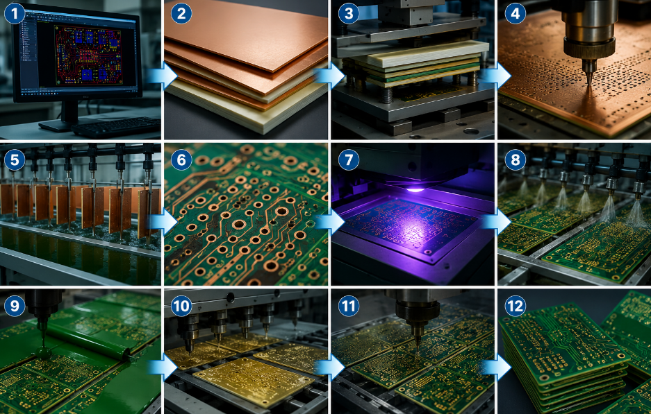
What is the Manufacturing Process of PCB in IoT?
The manufacturing process of PCB in IoT should control material, stack-up, impedance, antenna area, fine-pitch pads, surface finish, and electrical reliability. The process usually includes the following steps:
1. Engineering review
Check Gerber files, drill files, stack-up, copper thickness, solder mask, surface finish, impedance requirements, antenna keep-out area, and special production notes.
2. Material preparation
Select FR4, high-frequency material, flexible material, or rigid-flex material according to the product structure, RF requirements, thickness, and operating environment.
3. Inner layer production
Produce inner signal layers, ground layers, and power layers for multilayer IoT PCB. Check line width, spacing, copper quality, and layer defects before lamination.
4. Lamination
Press inner layers, prepreg, and copper foil into one board structure. Control board thickness, layer alignment, bonding strength, and warpage.
5. Drilling
Drill through holes, vias, and microvias according to the design file. Check hole size, position accuracy, burrs, and hole wall quality.
6. Copper plating
Plate copper inside holes and on the board surface. Control plating thickness, via reliability, hole wall coverage, and copper uniformity.
7. Outer layer circuit formation
Form the outer copper circuits through imaging, plating, and etching. Control RF traces, antenna areas, fine-pitch pads, and controlled impedance lines.
8. Solder mask application
Apply solder mask to protect copper traces. Check solder mask opening, bridge width, alignment, and clearance around fine-pitch ICs, RF modules, connectors, and test points.
9. Surface finish
Apply ENIG, HASL, OSP, immersion silver, or other surface finishes. For most IoT PCB projects, ENIG is often used for fine-pitch components and stable solderability.
10. Routing and profiling
Cut the PCB to the final shape. Check board outline, mounting holes, connector edges, panel breakaway points, and enclosure matching.
11. Electrical testing
Test open circuits, short circuits, net continuity, and controlled impedance when required. RF lines and high-speed signal paths should be checked carefully.
12. Final inspection
Inspect dimensions, appearance, solder mask, silkscreen, surface finish, hole quality, warpage, cleanliness, and packaging before assembly or shipment.
For manufacturing PCB in IoT, the key control points are controlled impedance, antenna keep-out area, fine-pitch pad accuracy, via reliability, surface finish quality, board thickness, and dimensional stability.
What Files and Requirements Should Be Checked Before IoT PCB Production?
Before IoT PCB production, confirm that files, component information, technical requirements, and testing needs are complete and consistent. This helps reduce file errors, production delays, and quality risks.
- Gerber files
Check copper layers, solder mask, silkscreen, board outline, drill data, and surface finish. - BOM
Confirm part numbers, quantities, package sizes, component values, brands, and approved alternatives. - PCB stack-up
Check layer count, material, board thickness, copper thickness, dielectric thickness, and impedance requirements. - Pick-and-place file
Confirm component coordinates, reference designators, rotation angles, and placement side if component mounting is required. - RF and antenna requirements
Confirm antenna keep-out area, RF trace control, impedance, grounding, and wireless module position. - Power requirements
Check input voltage, power rails, battery circuit, charging circuit, protection design, and current consumption targets. - Testing requirements
Confirm electrical test, impedance test, power-on test, RF communication test, sensor test, and current consumption test. - Packaging requirements
Confirm ESD packaging, moisture protection, labels, test records, and shipping requirements.
Before production, the key items to confirm are Gerber files, BOM, PCB stack-up, RF requirements, power requirements, testing methods, and packaging details.turer should confirm Gerber, BOM, pick-and-place file, assembly drawing, programming method, testing requirements, and special components to ensure smooth IoT PCB assembly.
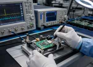
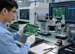
What Quality Tests Are Needed for PCB in IoT Devices?
Quality tests for PCB in IoT devices should check PCB quality, soldering quality, wireless performance, power consumption, sensor function, and final product reliability. IoT products often combine hardware, firmware, RF modules, and sensors, so visual inspection alone is not enough.
- Bare PCB electrical test
Check open circuits, short circuits, net continuity, and basic electrical connection before assembly. For RF or high-speed IoT PCB, controlled impedance testing may also be required. - Visual and dimensional inspection
Check board size, hole position, solder mask, silkscreen, surface finish, warpage, and appearance. This helps confirm that the PCB can fit the enclosure and assembly process. - SPI inspection
SPI checks solder paste volume, height, area, and position before SMT placement. It helps prevent insufficient solder, solder bridging, tombstoning, and open solder joints. - AOI inspection
AOI checks missing parts, wrong direction, component offset, polarity errors, solder bridges, and visible soldering defects after SMT assembly. - X-ray inspection
X-ray is used for BGA, QFN, LGA, shielded modules, and hidden solder joints. It helps find voids, poor solder joints, and hidden connection problems. - Firmware programming test
Confirm the correct firmware version, programming interface, and programming result. Firmware errors can cause communication failure, wrong sensor output, or abnormal power consumption. - Power-on and functional test
Check whether the board powers on correctly and whether basic circuits, interfaces, sensors, buttons, indicators, and connectors work as required. - RF communication test
Test Wi-Fi, Bluetooth, LoRa, LTE, NB-IoT, GPS, GNSS, UWB, Zigbee, or other wireless functions. This helps confirm signal strength, connection stability, and communication distance. - Current consumption test
Measure current in sleep mode, standby mode, active mode, and wireless transmission mode. This is important for battery-powered IoT devices. - Environmental and reliability test
For outdoor, industrial, or long-life IoT products, temperature, humidity, vibration, ESD, surge, and burn-in tests may be required.
The test plan should match the real application. A simple smart sensor may need basic function and current testing, while an industrial IoT device may require stronger RF, protection, and reliability testing.
What Common Problems Occur in PCB for IoT Projects?
Common problems in PCB for IoT projects usually come from poor RF layout, unstable power design, incomplete files, weak assembly control, or insufficient testing. These issues may not appear during simple power-on tests, but they can cause failure in real use.
- Weak wireless signal
This is often caused by poor antenna placement, blocked antenna keep-out area, incorrect RF trace routing, or metal parts near the antenna. The solution is to review RF layout early and test the board inside the final enclosure. - Short battery life
High standby current, unsuitable regulators, poor sleep mode support, and wrong component selection can reduce battery life. Current consumption should be tested in different working modes. - Unstable sensor data
Sensors may be affected by heat sources, power noise, poor grounding, or wrong placement. Temperature sensors, motion sensors, and environmental sensors should be placed according to their actual working conditions. - Power reset or boot failure
Wireless modules may draw high peak current during transmission. If the power circuit cannot support it, the device may reset or disconnect. Power rails and peak current capacity should be checked during design and testing. - Soldering defects
Fine-pitch ICs, small passive components, and dense layouts may cause solder bridges, tombstoning, insufficient solder, and component shift. SPI, AOI, X-ray, and proper stencil design help reduce these defects. - Wrong component direction or polarity
LEDs, diodes, ICs, connectors, batteries, and modules may fail if polarity or direction is wrong. Clear silkscreen, assembly drawings, and first-article inspection are important. - Missing test points
Without enough test points, firmware programming, debugging, and mass production testing become difficult. Test points should be planned for power rails, programming pins, communication interfaces, and key signals. - BOM or component sourcing problems
Wrong package, unavailable parts, unapproved substitutes, or unclear part numbers can delay production. BOM should be reviewed before assembly, and any replacement should be confirmed before use. - Poor enclosure fit
The PCB may work on the bench but fail after installation due to blocked antenna, wrong connector position, component height conflict, or battery interference. Mechanical design should be checked before production. - Inconsistent mass production quality
A prototype may work well, but batch production can fail if the process is not controlled. DFM review, first-article inspection, test fixtures, and clear production standards help improve consistency.
To reduce these problems, the project should confirm RF layout, power design, test points, BOM, enclosure fit, assembly requirements, and test plan before mass production.
Where is PCB in IoT Commonly Used?
PCB in IoT is used in connected devices that collect data, control systems, and transmit information. Common applications include:
- Smart home devices
Smart locks, thermostats, lighting controls, gateways, and sensors. - Industrial IoT equipment
Monitoring modules, controllers, gateways, and data collection devices. - Wearable electronics
Smart watches, health bands, portable sensors, and compact monitors. - Medical monitoring devices
Wearable sensors, remote monitors, and portable diagnostic devices. - Asset tracking devices
GPS trackers, BLE tags, logistics trackers, and fleet monitoring devices. - Access control systems
Smart locks, card readers, door controllers, and biometric devices. - Smart agriculture devices
Soil sensors, weather stations, and irrigation controllers. - Smart meters
Water meters, gas meters, electricity meters, and energy monitoring devices. - Environmental monitoring devices
Air quality sensors, temperature and humidity monitors, and gas detectors.
How to Choose a Reliable PCB Manufacturer for IoT Devices?
Choosing a reliable PCB manufacturer for IoT devices should focus on RF control, assembly capability, component sourcing, testing support, and stable delivery. IoT products often include wireless modules, sensors, batteries, and compact layouts, so the supplier must be able to control both PCB fabrication and assembly quality.
- Check IoT PCB experience
Ask whether the manufacturer has produced PCBs for smart sensors, gateways, trackers, access control devices, wearable devices, or industrial IoT modules. These products usually involve antenna areas, low-power circuits, small components, and functional testing. - Confirm RF and antenna capability
The supplier should understand antenna keep-out areas, controlled impedance, RF trace routing, grounding, shielding, and enclosure impact. This is important for Wi-Fi, Bluetooth, LoRa, LTE, NB-IoT, GPS, GNSS, UWB, and Zigbee products. - Review PCB manufacturing capability
Check whether the supplier can support multilayer PCB, fine-pitch pads, small vias, ENIG surface finish, controlled impedance, and stable board thickness. These details affect SMT assembly, wireless performance, and long-term reliability. - Choose PCB fabrication and assembly together
IoT projects often require PCB manufacturing, SMT assembly, component sourcing, firmware programming, and testing. A one-stop supplier can reduce file mismatch, BOM errors, component delays, and unclear responsibility. - Ask for DFM and DFT review
The manufacturer should review Gerber files, BOM, pick-and-place files, pad sizes, component spacing, panelization, polarity marks, and test points before production. This helps avoid assembly defects and testing difficulties. - Check component sourcing control
IoT PCB projects often use wireless modules, MCUs, sensors, crystals, connectors, batteries, and protection parts. The supplier should confirm part availability, package accuracy, lifecycle status, and approved alternatives before assembly. - Confirm testing capability
The supplier should support AOI, SPI, X-ray inspection, electrical testing, firmware programming, RF communication testing, current consumption testing, and functional testing. For IoT devices, visual inspection alone is not enough. - Check prototype and revision support
IoT products often need prototype testing and design updates. The supplier should support small-batch production, issue feedback, design revision checks, and stable transition to mass production. - Review quality control process
Check how the supplier controls incoming materials, PCB fabrication, solder paste printing, SMT placement, reflow soldering, inspection, testing, and final packaging. Stable quality control helps reduce field failure. - Evaluate delivery and communication
Choose a supplier that confirms BOM updates, firmware changes, testing requirements, and packaging details clearly. Realistic lead times and fast response help avoid repeated delays and rework.
A reliable PCB manufacturer for IoT devices should help control PCB quality, SMT assembly accuracy, wireless performance, power stability, testing coverage, and production consistency from prototype to mass production.
FAQs About PCB in IoT
Q1: What is the difference between PCB in IoT and a normal PCB?
A1: PCB in IoT usually requires stronger attention to wireless communication, low power design, sensor accuracy, firmware programming, and functional testing.
Q2: Does every IoT PCB need RF design control?
A2: Not every IoT PCB has complex RF circuits, but any board with Wi-Fi, Bluetooth, LoRa, LTE, GPS, GNSS, UWB, or Zigbee should control antenna layout, RF traces, and grounding.
Q3: Is a 2-layer PCB enough for IoT devices?
A3: A 2-layer PCB may be enough for simple IoT devices. For better EMI control, RF stability, dense routing, or power distribution, 4-layer or 6-layer PCB is usually better.
Q4: Why is current consumption testing important for IoT PCB?
A4: Many IoT devices are battery-powered. Current testing helps confirm battery life in sleep mode, standby mode, active mode, and wireless transmission mode.
Q5: What should be checked before IoT PCB assembly?
A5: Gerber files, BOM, pick-and-place file, component polarity, RF module position, antenna keep-out area, test points, firmware version, and functional test requirements should be checked.
Q6: What causes wireless failure in IoT PCB projects?
A6: Common causes include poor antenna placement, blocked keep-out area, wrong RF trace design, power noise, metal enclosure interference, and lack of final RF testing.
Q7: Can IoT PCB manufacturing and assembly be done by one supplier?
A7: Yes. A one-stop PCB and assembly supplier can reduce file mismatch, BOM errors, communication delays, and responsibility gaps during production.
Q8: What files are needed for an IoT PCB quotation?
A8: Gerber files, BOM, pick-and-place file, assembly drawing, test requirements, firmware programming instructions, and special notes are usually needed for an accurate quotation.
Start Your IoT PCB Project with EBest
If you are developing an IoT product, EBest can support your project from PCB manufacturing, component sourcing, SMT assembly, firmware programming support, functional testing, and final inspection. We help customers reduce production risks and improve quality from prototype to mass production.
Send your Gerber files, BOM, pick-and-place file, and testing requirements to sales@bestpcbs.com. Our team will review your IoT PCB project and provide a fast quotation with practical manufacturing and assembly suggestions.