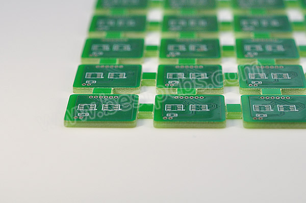
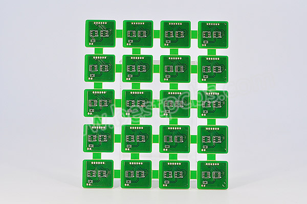
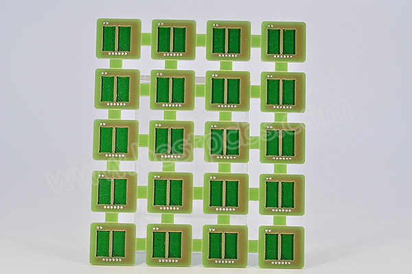
Board level shielding is used to control EMI and RF noise directly on a PCB. It protects sensitive circuits, limits interference between nearby components, and helps electronic products meet EMC requirements before final testing.
This shielding method is common in RF modules, wireless products, medical electronics, automotive control boards, industrial devices and compact consumer electronics. A good design is not only about placing a metal can over a circuit. It must work together with PCB layout, grounding, material selection, aperture control, venting holes and assembly quality.
This guide explains how PCB level shielding works, which shield can structures are commonly used, how to select materials, and what design rules affect shielding effectiveness in PCB manufacturing and PCBA assembly.
What Is Board Level Shielding?
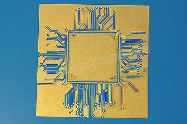
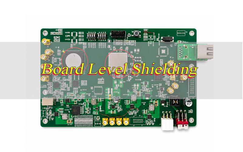
Board level shielding is a metal shield structure mounted directly on a PCB to reduce electromagnetic interference around selected circuits. It is also called PCB level shielding, board level EMI shielding, PCB board level shielding, board level shield or BLS shielding.
The shield usually covers RF chips, oscillators, power circuits, sensors, high-speed ICs or other noise-sensitive areas. Together with the PCB ground plane, the metal shield forms a local barrier that limits electromagnetic energy from entering or leaving the protected circuit area.
Unlike full enclosure shielding, this method controls EMI near the source. This makes it useful for compact PCB designs where different functional circuits are placed close together.
Why Is Board Level Shielding Used on PCBs?
This shielding method is used on PCBs to reduce EMI, improve signal stability, protect sensitive components and support EMC compliance. In modern electronic products, high-speed signals, wireless circuits and switching power supplies often operate on the same PCB, creating more coupling risk.
A shield can help isolate RF sections, clock circuits, DC-DC converters, analog front ends and sensor areas. It also reduces the chance that one circuit will interfere with another circuit during normal operation.
For manufacturing projects, stable EMI performance reduces redesign risk, certification delay, field failure and product return risk. It is especially valuable when the product must meet FCC, CE, CISPR, EN 55032 or project-specific EMC requirements.
How Does Board Level EMI Shielding Work?
Board level EMI shielding works by reflecting, absorbing and grounding electromagnetic energy. When EMI reaches the metal shield, part of the energy is reflected by the conductive surface, part is absorbed by the material, and the remaining current is directed to ground.
The shield can forms the top and side walls of the protected area, while the PCB ground plane works as the bottom reference. This creates a small Faraday cage around the circuit.
However, the shield only works well when it has a low-impedance ground connection. Poor grounding, long seams, large holes or broken ground pads can allow EMI leakage and reduce shielding effectiveness.
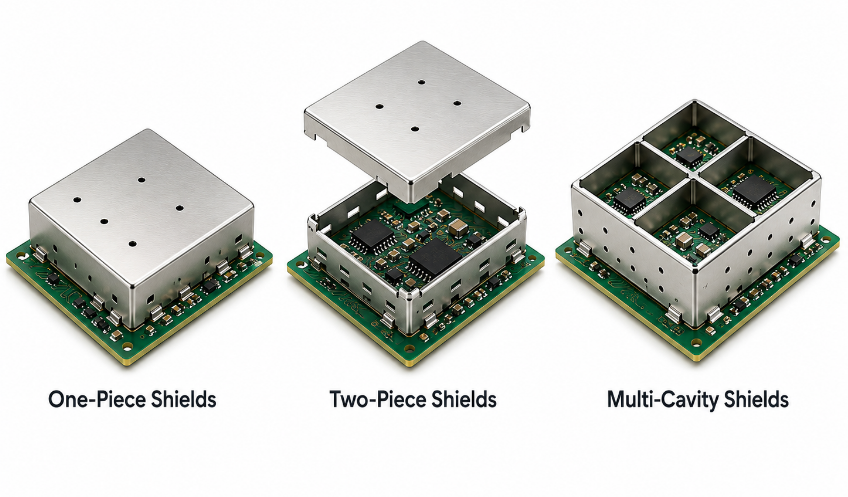
What Are the Common Types of Board Level Shielding Cans?
Common board level shielding cans can be divided by structure into one-piece shields, two-piece shields and multi-cavity shields. This classification uses the same standard: how the metal shield is physically built and accessed.
| Type | Structure | Best Fit | Limitation |
|---|---|---|---|
| One-piece shield | Fixed single metal cover | Low cost, compact layout, mass production | Difficult rework after soldering |
| Two-piece shield | Soldered frame plus removable cover | Debugging, RF tuning, repair access | Higher part cost and more height control |
| Multi-cavity shield | One shield with internal partitions | Several RF or mixed-signal zones in one area | More complex tooling and grounding |
Surface mount shielding is a mounting method, not a structural type. Custom board level shielding is a manufacturing option, not a separate can structure. Keeping the classification consistent makes selection easier and avoids mixing different standards.
What Is the Difference Between One Piece and Two Piece Board Level Shielding?
One-piece shielding focuses on cost and compact production, while two-piece shielding focuses on access and serviceability. The choice should match the product stage, RF tuning requirement, rework plan and cost target.
| Item | One-Piece Shield | Two-Piece Shield |
|---|---|---|
| Structure | Single soldered cover | Soldered frame plus removable lid |
| Cost | Lower | Higher |
| PCB space | More compact | Slightly larger |
| Assembly | Simple SMT soldering | Frame soldering plus cover fitting |
| Rework | Harder to remove | Easier access after assembly |
| RF tuning | Less convenient | Better for tuning and inspection |
| Production fit | Stable mass production | Prototype, RF module, repairable design |
| Main risk | Damage during removal | Lid looseness or contact variation |
For stable high-volume products, one-piece shielding is usually more economical. For wireless modules, prototypes and circuits that may require adjustment after assembly, two-piece shielding is more practical.
When Should You Use Multi-Cavity Board Level Shielding?
Multi-cavity board level shielding should be used when several circuits on the same PCB need separate EMI isolation within limited space. Instead of using multiple separate cans, one shield body uses internal walls to divide different circuit areas.
This structure is useful for RF transmit and receive paths, GPS, WiFi, Bluetooth, LTE, clock circuits, analog circuits and power sections placed close together.
Main use cases include:
- Separating RF input and output stages.
- Isolating noisy power circuits from sensitive signals.
- Reducing coupling between wireless modules.
- Saving PCB space compared with several independent shields.
- Improving assembly efficiency in compact products.
The internal walls must be properly grounded. If the partitions are not connected to ground, cavity-to-cavity leakage may still occur.
How to Select Board Level Shielding Materials?
Board level shielding material selection should consider EMI performance, frequency range, solderability, corrosion resistance, forming difficulty and cost. Common materials include tin-plated steel, nickel silver, copper alloy, stainless steel and aluminum.
| Material | Feature | Manufacturing Fit | Typical Use |
|---|---|---|---|
| Tin-plated steel | Good shielding and solderability | Stamping, low cost | General PCB shield cans |
| Nickel silver | Corrosion resistant and solderable | Stable forming | RF modules, durable electronics |
| Copper alloy | High conductivity | May need plating | High-performance EMI shielding |
| Stainless steel | Strong and corrosion resistant | Harder to form | Harsh environments |
| Aluminum | Lightweight and conductive | Poor direct solderability | Special enclosure designs |
Tin-plated steel is widely used for cost-effective PCB shield cans. Nickel silver is suitable when appearance, corrosion resistance and solderability matter. Copper alloy is better for high-performance EMI & RFI board level shielding, but it usually increases material cost.
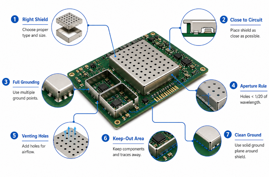
How to Design Board Level Shielding for PCB Layout?
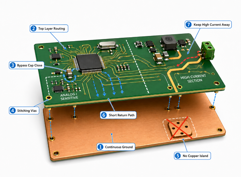
Shield design should start during PCB layout, not after EMI failure. The shield footprint, ground pads, component clearance, via stitching and assembly process must be planned before prototype production.
Step 1: Define the protected circuit area.
Place the noisy or sensitive circuit inside a clear shield boundary. RF chips, oscillators, switching regulators, high-speed ICs and analog front ends should not be mixed without purpose. A clear boundary helps control coupling and simplifies shield can design.
Step 2: Reserve enough mechanical clearance.
The shield wall should not touch components, solder joints or tall parts. Clearance should include component tolerance, shield tolerance, solder paste thickness, PCB warpage and possible lid deformation. A 3D PCB model should be checked before tooling.
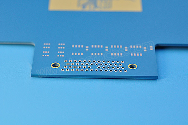
Step 3: Create a continuous ground pad ring.
The shield footprint should use exposed ground pads around the shield perimeter. Avoid broken pads, narrow necks or isolated copper islands. A continuous pad ring improves soldering stability and reduces EMI leakage through the shield base.
Step 4: Add ground vias near the shield wall.
Ground vias should connect the shield pad ring to the main ground plane. For high-frequency circuits, via spacing should be tighter because long gaps behave like EMI leakage paths. The vias should be placed close to the shield wall instead of far inside the PCB.
Step 5: Keep critical traces away from shield gaps.
High-speed traces, RF lines and clock signals should not cross shield seams or openings. If a signal must enter or leave the shielded area, use controlled routing, filtering or ground reference continuity to reduce noise leakage.
Step 6: Check antenna and keep-out areas.
Grounded shield metal can detune antennas or reduce radiation efficiency. Antenna keep-out areas should stay clear unless the RF design intentionally includes the shield as part of the ground structure.
Step 7: Review assembly and inspection access.
The footprint should support solder paste printing, SMT placement, reflow soldering and visual inspection. Best practices for board level shielding are effective only when the PCB layout, shield structure and PCBA process are checked together.
How to Ground Board Level Shielding on a PCB?
The shield must connect to a continuous, low-impedance ground path around the protected area. If the shield has only a few weak ground points, EMI can leak through seams and openings.
Step 1: Use a solid ground reference under the shield.
The PCB ground plane should remain continuous below the shielded area. Split planes, slots or broken return paths under the shield can reduce EMI control and create unexpected coupling.
Step 2: Connect the shield frame to exposed ground pads.
Most PCB shield cans are soldered directly to exposed copper pads connected to ground. These pads should be wide enough for stable solder joints and should not be covered by solder mask.
Step 3: Place stitching vias close to the shield wall.
Ground vias should be placed near the soldered shield pads to reduce inductance. For RF products, closer via spacing gives better high-frequency grounding and reduces leakage through the shield perimeter.
Step 4: Avoid random split-ground connections.
The shield should not be connected to different ground regions without checking return current flow. Poor ground strategy can create noise paths, ESD issues or ground loop risk.
Step 5: Keep the ground path short and direct.
The shield current should return to the main ground plane through the shortest practical path. Long thin traces between the shield and ground reduce performance because they add impedance at high frequency.
Step 6: Confirm continuity after assembly.
After soldering, the shield-to-ground path should be checked by inspection and electrical continuity testing. Poor wetting, solder voids or lifted shield tabs can weaken the final grounding result.
What Is the Board Level Shielding Aperture Size Rule?
The aperture size rule is simple: holes, slots, seams and gaps should be much smaller than the wavelength of the highest problem frequency. Long narrow openings leak more EMI than small round openings, even when the total open area looks similar.
| Frequency | Wavelength | Safer Opening Target | Design Note |
|---|---|---|---|
| 300 MHz | 1000 mm | Below 50 mm | Avoid long slots |
| 1 GHz | 300 mm | Below 15 mm | Use dense grounding |
| 2.4 GHz | 125 mm | Below 6 mm | Control seams carefully |
| 5 GHz | 60 mm | Below 3 mm | Minimize apertures |
The longest opening dimension is usually the key risk. For RF designs, one large vent slot is usually worse than several small round holes. The final size should be checked with the operating frequency, shield height, cavity shape and shielding effectiveness target.
How Should Venting Holes Be Designed in PCB Shield Cans?
PCB shield can venting holes design should release heat, flux vapor and trapped air without creating large EMI leakage paths. Hole size, hole shape and hole position all affect soldering reliability and shielding performance.
- Use several small holes instead of one large opening.
Small distributed holes reduce gas trapping during reflow while limiting EMI leakage compared with long slots. - Prefer round holes or short openings.
Long narrow slots are more likely to act as slot antennas, especially in RF and high-speed digital products. - Keep holes away from RF hot spots.
Venting holes should not sit directly above RF traces, antennas, oscillators or high-noise switching nodes. - Balance venting with shielding effectiveness.
More holes improve gas release and thermal relief, but too much open area reduces EMI performance. - Consider pick-and-place stability.
Hole placement should not affect vacuum nozzle pickup, shield flatness or SMT placement accuracy. - Review holes before tooling.
Once a stamped shield tool is made, changing venting hole size or location can increase cost and delay production.
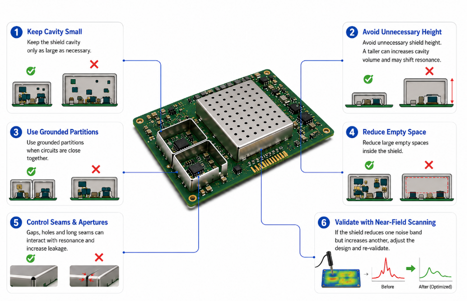
How to Prevent Board Level Shielding Resonance?
Board level shielding resonance can occur when the shield cavity supports standing waves at certain frequencies. The result may be poor EMI reduction or new noise peaks after the shield is installed.
- Keep the shield cavity only as large as necessary.
Oversized cavities increase resonance risk and may reduce performance at higher frequencies. - Avoid unnecessary shield height.
A taller can creates a larger internal cavity and may shift resonance into a problematic frequency band. - Use grounded partitions when circuits are close together.
Multi-cavity shielding can reduce internal coupling and help control resonance between functional zones. - Reduce large empty spaces inside the shield.
Empty volume can support stronger cavity modes. Component placement and internal wall design should be reviewed together. - Control seams and apertures.
Gaps, holes and long seams can interact with cavity resonance and increase radiated leakage. - Validate with near-field scanning.
If the shield reduces one noise band but increases another, the cavity size, grounding, partition design or aperture layout should be adjusted.
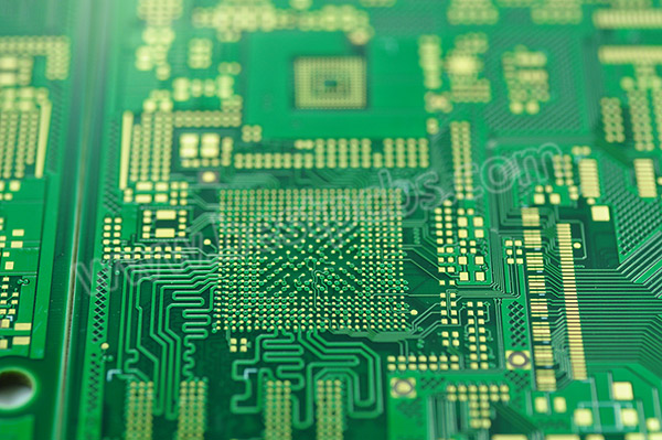
What Factors Affect Board Level Shielding Effectiveness?
Shielding effectiveness is affected by material, thickness, conductivity, permeability, grounding, seams, apertures, cavity size and assembly quality. A good material alone cannot guarantee good EMI performance.
Important factors include:
- Shield material and plating quality.
- Metal thickness and mechanical rigidity.
- Ground pad continuity around the shield wall.
- Via stitching density near the shield perimeter.
- Aperture size, venting holes and seam length.
- Shield height and cavity size.
- Distance between shield wall and noisy components.
- Solder joint quality and shield coplanarity.
- PCB ground plane integrity and stack-up design.
In mass production, EMI performance depends on both design and process control. A small soldering defect, bent wall or poor ground connection can reduce the final shielding result.
Where Is Board Level Shielding Commonly Used?
Board level shielding is commonly used in electronic products where RF, high-speed, power and sensitive analog circuits share the same PCB. It is especially useful when the product has limited space and strict EMI requirements.
Common applications include:
- WiFi, Bluetooth, GPS, LTE and 5G wireless modules.
- RF front-end circuits and antenna matching sections.
- Switching power supplies and DC-DC converters.
- Medical monitoring and diagnostic electronics.
- Automotive control modules and battery systems.
- Industrial controllers, robotics and automation boards.
- IoT gateways, smart terminals and wearable devices.
- Telecom, networking and high-speed digital equipment.
For medical and automotive projects, traceability and reliability are usually more important. For consumer IoT products, compact size, cost control and repeatable SMT yield are often the main concerns.
When Do You Need Custom Board Level Shielding?
Custom board level shielding is needed when standard shield cans cannot match the PCB layout, component height, EMI target or assembly requirements. Standard cans work for simple rectangular areas, but many modern PCB designs need special shapes or internal partitions.
Custom board level EMI RF shield support is useful when:
- The PCB has limited space or irregular component placement.
- The shield height must match a tight enclosure.
- Multiple circuits need separate cavities.
- Venting holes must avoid sensitive RF areas.
- The design requires one-piece or two-piece shielding options.
- The project needs stable OEM/ODM mass production.
- Standard shield cans cannot meet the required footprint or grounding method.
For custom projects, the quotation package should include Gerber files, PCB stack-up, component height data, 3D files, quantity, material preference and EMI concerns. This helps review fit, tooling, solderability and production risk before sampling.
FAQs About Board Level Shielding
Q1: Can board level shielding cans be assembled by standard SMT reflow?
A1: Yes. Most board level shielding cans can be assembled by SMT reflow when the footprint, solder paste opening and coplanarity are correct. The shield tabs should sit flat on exposed ground pads. Poor flatness or insufficient solder paste can cause weak grounding, tilted cans or EMI leakage after assembly.
Q2: Should solder mask be opened under shield can pads?
A2: Yes. Shield can pads should have exposed copper for stable solder wetting and low-impedance grounding. If solder mask covers the pad area, the shield may not bond correctly to ground. This can weaken mechanical strength and reduce EMI performance, especially for RF or high-speed PCB designs.
Q3: What surface finish is suitable for PCB shield can soldering?
A3: ENIG, immersion tin, HASL and lead-free HASL can be used depending on the PCB process. The key requirement is stable solderability on the exposed shield pads. For fine-pitch, RF or high-reliability designs, ENIG is often selected because it offers flat surface quality and good storage stability.
Q4: Can a PCB shield can be removed after soldering?
A4: Yes, but removal can damage pads, nearby components or solder mask if not controlled. One-piece shield removal is harder because the full can must be heated and lifted. Two-piece shielding is easier because the lid can be removed while the frame stays soldered to the PCB.
Q5: How does shield height affect PCB shielding performance?
A5: Shield height affects cavity volume, resonance risk, mechanical stiffness and enclosure clearance. A taller shield gives more component clearance but may increase resonance risk. A lower shield saves space and reduces cavity volume, but it must still leave enough clearance above the tallest component.
Q6: Can shield cans cause short circuits on a PCB?
A6: Yes. Short circuits can occur if the shield touches components, exposed pads, vias or solder joints inside the covered area. The design should reserve safe internal clearance, avoid exposed copper near shield walls and check tolerance stack-up before tooling. A 3D file review helps reduce this risk.
Q7: What is the difference between a PCB shield can and an enclosure shield?
A7: A PCB shield can controls EMI around a selected circuit area on the board. An enclosure shield controls EMI at the product housing level. PCB shield cans are better for local noise control, while enclosure shielding is better for whole-product protection. Many products use both methods together.
Q8: Does BLS shielding help with both EMI and RFI?
A8: Yes. BLS shielding can reduce both EMI and RFI when the material, grounding and aperture design match the frequency range. EMI includes broader interference from digital, power and RF sources. RFI focuses on radio-frequency interference, so RF products usually need tighter grounding and smaller openings.
Q9: Can board level shields improve ESD protection?
A9: They can help when connected to a defined ground or chassis strategy. A grounded shield can provide a discharge path and protect sensitive circuits from nearby ESD events. However, it should not be treated as the only ESD solution. TVS devices, grounding, spacing and enclosure design are still important.
Q10: What causes poor solder joints on PCB shield cans?
A10: Common causes include uneven shield tabs, poor pad design, insufficient solder paste, oxidation, wrong reflow profile and PCB warpage. Poor solder joints reduce both mechanical strength and EMI grounding quality. Pad size, paste aperture, coplanarity and material plating should be checked before mass production.
Q11: Can shielding cans be used on both rigid and rigid-flex PCBs?
A11: Yes, but the soldered shield area should normally stay on the rigid section. Shield cans are not suitable for bending areas because mechanical stress can crack solder joints or deform the metal. For rigid-flex PCB designs, the shield footprint should be placed away from bend zones.
Q12: What files are needed for custom board level shielding?
A12: A complete file package should include Gerber files, PCB stack-up, component height data, 3D files, shield outline, target material, surface finish, quantity and EMI concern. Component height and shield footprint data are especially important. Clear files reduce tooling errors and improve sample accuracy.
Q13: Is nickel silver better than tin-plated steel for PCB shield cans?
A13: Nickel silver offers better corrosion resistance and clean appearance, while tin-plated steel is usually more cost-effective. The better choice depends on environment, solderability, cost target and EMI requirement. For many general PCB shield cans, tin-plated steel is enough. For durable RF modules, nickel silver is often considered.
Q14: Can shield cans affect PCB thermal performance?
A14: Yes. A shield can may trap heat if the covered circuit has high power loss. Venting holes, copper area, thermal vias and component placement should be reviewed together. For switching regulators or RF power circuits, shielding and thermal design should be checked before final layout approval.
Q15: What affects the cost of custom PCB shield cans?
A15: Cost is affected by material, shield size, wall height, cavity count, tooling method, tolerance, surface finish, order volume and assembly process. Multi-cavity, tight tolerance and special materials usually increase cost. The best option should balance EMI performance, manufacturability and long-term production stability.
Conclusion
The technical point is that PCB shielding only works well when material selection, grounding, aperture control, PCB layout and assembly quality are designed as one system. A shield can is not a simple cover for fixing poor routing, weak grounding or uncontrolled return paths. For reliable EMI performance, the shield footprint, ground vias, venting holes, cavity size and testing method should be planned before prototype production.
For selection, use one-piece shielding for cost-sensitive mass production, two-piece shielding for debugging and RF tuning, and multi-cavity shielding for compact circuits that require internal isolation. For custom PCB, PCBA and board level shielding solutions from a China source factory, send your project files and requirements to EBest Circuit via sales@bestpcbs.com for a quotation.