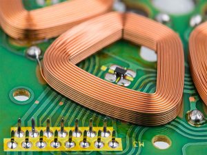
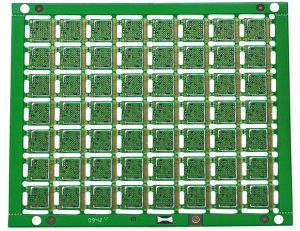
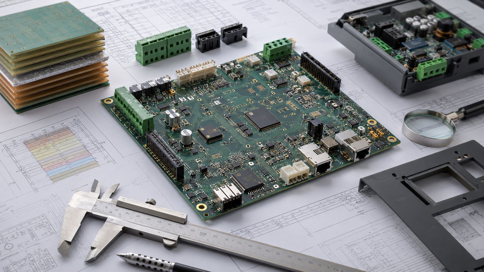
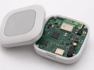
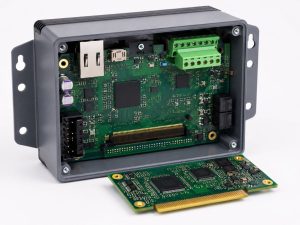
Commercial PCBs are used in electronic products that need stable performance, controlled cost, and repeatable production quality. They are widely applied in consumer devices, communication products, lighting systems, control modules, and general electronic equipment.
For buyers, the key is not only getting a working prototype. The real goal is to move from commercial PCB prototype fabrication to stable commercial printed circuit board production with reliable fabrication, clean assembly, strict inspection, and predictable delivery.
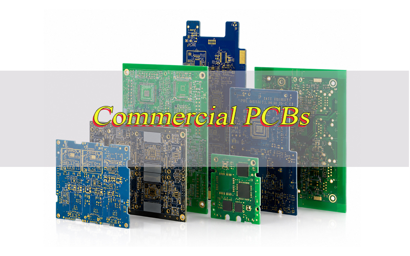
What Are Commercial PCBs?
Commercial PCBs are printed circuit boards used in everyday electronic products, business devices, communication equipment, lighting systems, and control electronics. They provide the electrical connection and mechanical support for components such as ICs, resistors, capacitors, connectors, LEDs, and sensors.
Commercial PCBs usually focus on stable function, cost control, manufacturability, and repeatable batch quality. They do not always require aerospace-level testing, but they still need reliable materials, accurate circuit formation, good solderability, and consistent inspection.
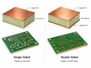
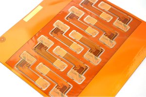
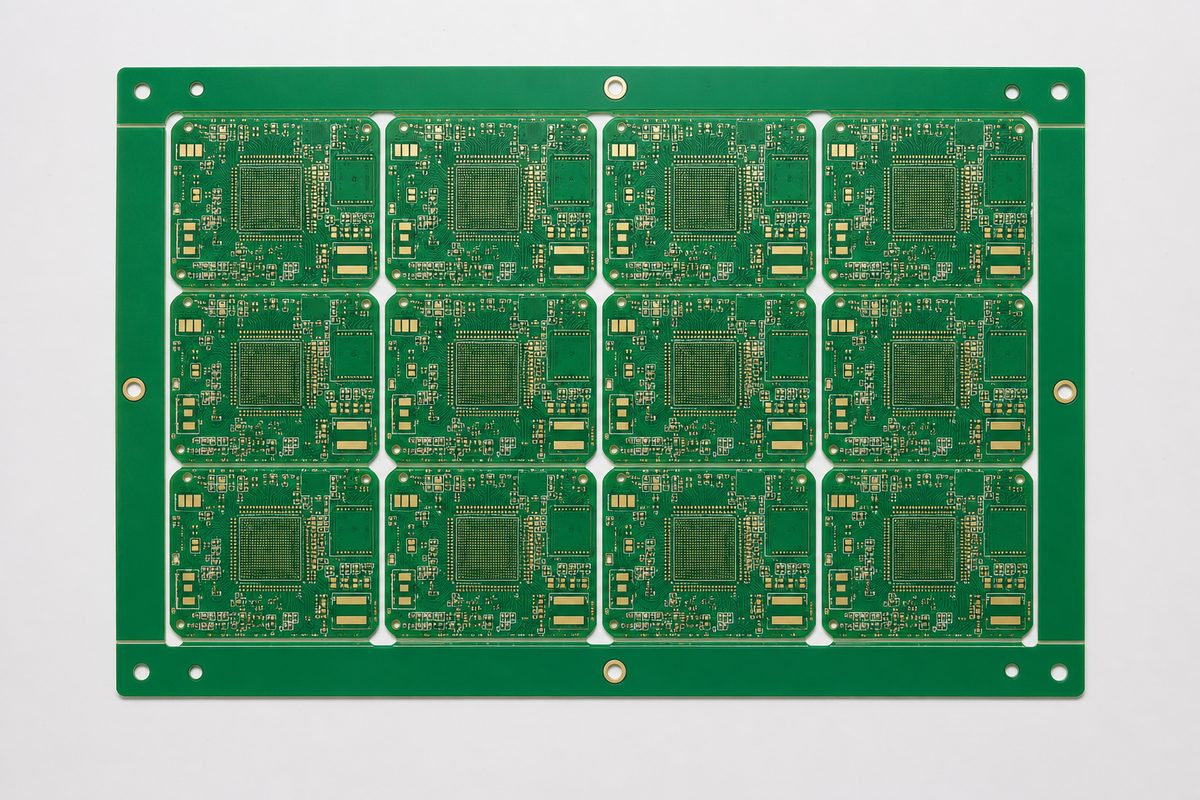
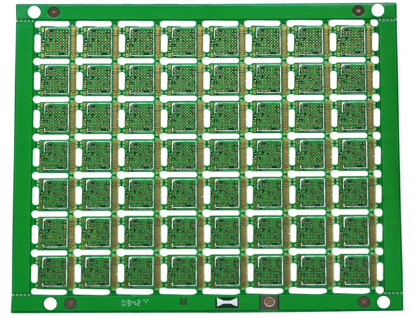
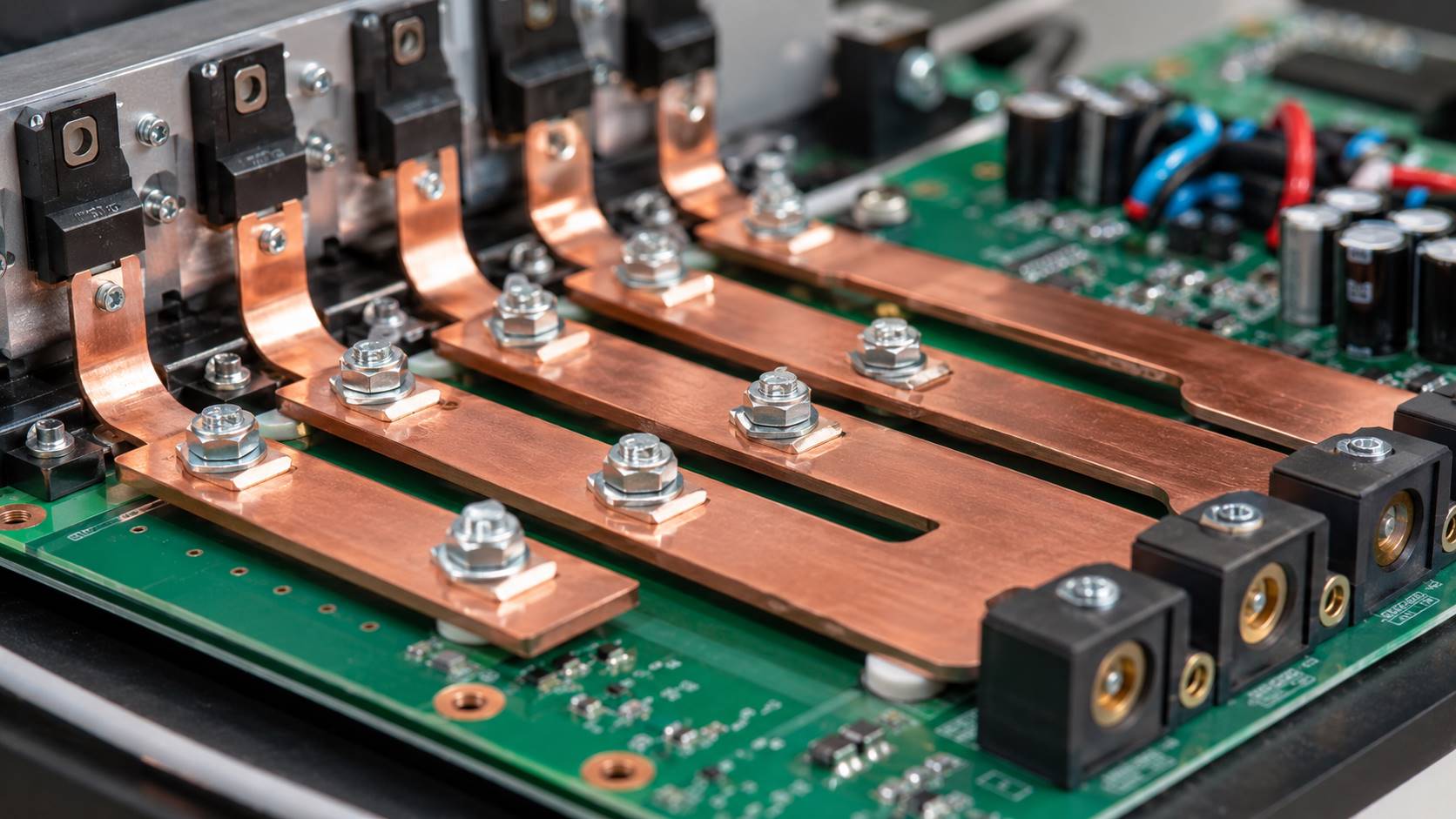
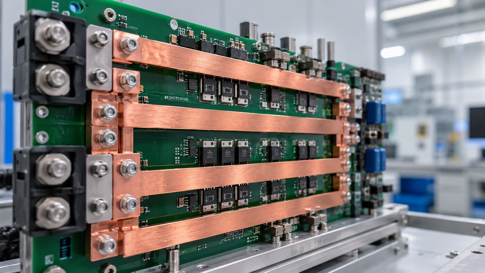
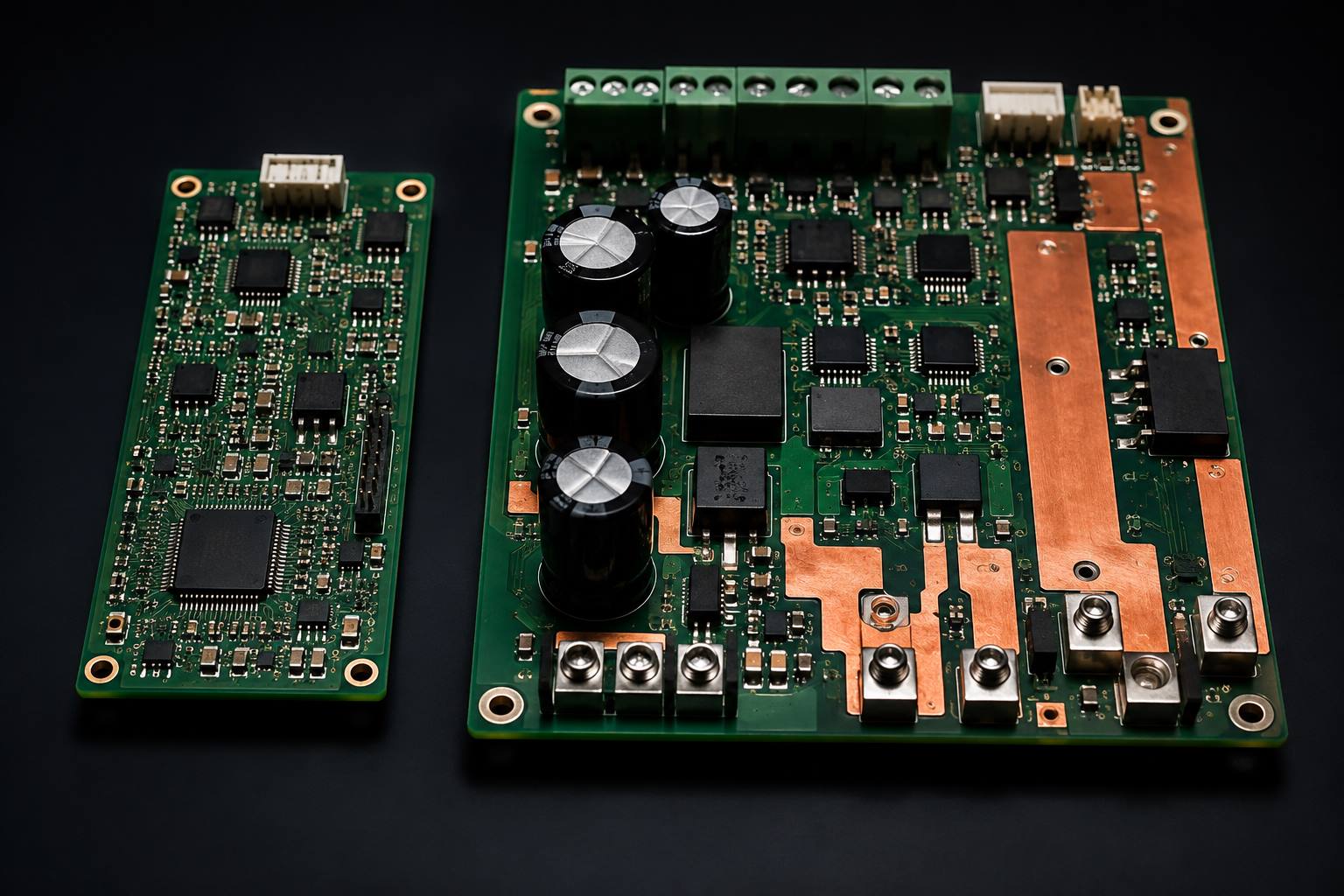
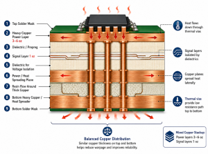
Common commercial PCB board types include single-sided PCB, double-sided PCB, multi layer commercial PCB, aluminum PCB, flexible PCB, rigid-flex PCB, and assembled PCBA. The correct choice depends on product function, operating environment, board size, current load, signal speed, and order quantity.
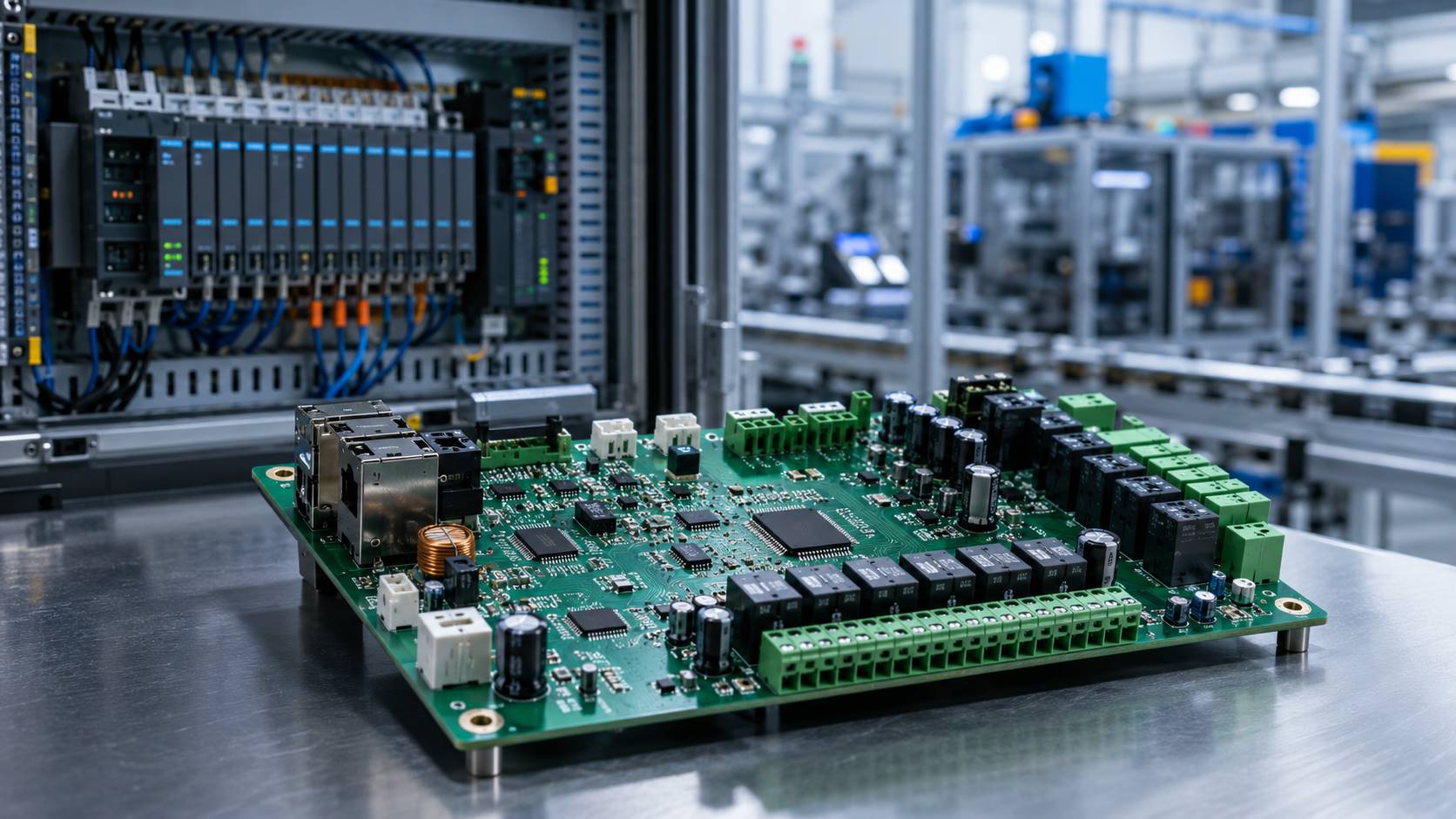
Where Are Commercial PCB Boards Commonly Used?
Commercial PCB boards are used in products that require reliable electronic control at a practical production cost. These boards support both simple electronic circuits and more complex products with power, signal, communication, and control functions.
Typical applications include:
- Consumer electronics: smart home devices, chargers, audio products, display modules, and handheld devices.
- Communication products: routers, gateways, antenna modules, IoT devices, and signal control boards.
- LED lighting: LED drivers, commercial lamps, lighting control systems, and signage products.
- Business equipment: POS machines, access control systems, printers, meters, and display panels.
- Industrial-lite electronics: sensors, controllers, power modules, automation accessories, and control panels.
- Medical and wellness devices: portable monitoring devices, diagnostic accessories, and non-implant electronic modules.
- Automotive accessories: lighting modules, chargers, control boards, and aftermarket electronic devices.
In short, commercial PCBs are suitable for products that need stable performance, reasonable cost, and scalable production.
What Materials Are Commonly Used for Commercial Grade PCB Boards?
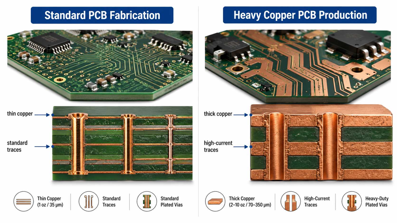
Commercial grade PCB boards usually use FR-4, high-Tg FR-4, aluminum base, polyimide, copper foil, solder mask, and common surface finishes. Material selection affects heat resistance, solderability, insulation strength, mechanical stability, cost, and product life.
| Material | Common Use | Key Point |
|---|---|---|
| FR-4 | Standard commercial PCB board | Cost-effective and widely used |
| High-Tg FR-4 | Higher temperature products | Better thermal stability |
| Aluminum Base | LED and power boards | Improved heat dissipation |
| Polyimide | Flexible PCB | Good bending resistance |
| Copper Foil | Conductive layers | Affects current capacity |
| HASL | General products | Economical surface finish |
| ENIG | Fine-pitch assembly | Flat pads and good solderability |
| OSP | Short-cycle production | Flat and low-cost finish |
For most commercial PCB manufacturing projects, FR-4 is the standard material choice. However, LED products, compact electronics, power modules, and products with higher working temperature may need high-Tg FR-4, thicker copper, aluminum substrate, or ENIG surface finish.
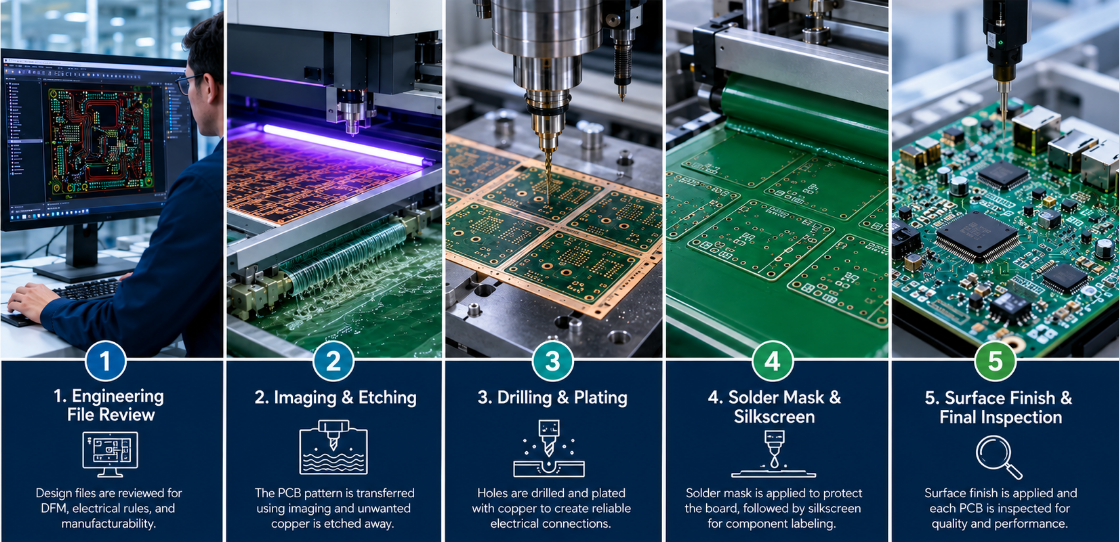
How Are Commercial PCBs Made?
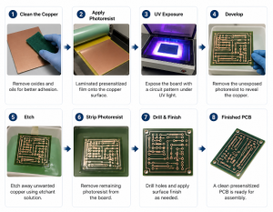
Commercial PCBs are made through file review, material preparation, circuit formation, drilling, plating, solder mask, surface finish, profiling, and final testing. Each step affects board accuracy, solderability, and batch production stability.
- Engineering file review: The manufacturer checks Gerber files, drill files, stackup, copper thickness, board thickness, solder mask, silkscreen, and panel requirements. This helps find missing data, wrong hole sizes, unclear tolerances, or production risks before fabrication starts.
- Material preparation: FR-4 is commonly used for commercial PCB manufacturing. For products with higher heat, power, or mechanical requirements, high-Tg FR-4, aluminum base, or thicker copper may be selected.
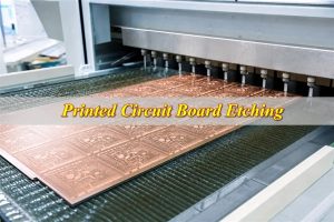
- Circuit imaging and etching: The copper layer is coated, exposed, developed, and etched to form the required circuit pattern. For multi layer commercial PCB production, inner layers are processed first before lamination.
- Lamination and drilling: Inner layers, prepreg, and copper foil are pressed together under heat and pressure. Then vias, through holes, and mounting holes are drilled according to the design files.
- Copper plating: Copper is plated onto hole walls and outer layers to build electrical connection between layers. Good plating quality is important for conductivity, via reliability, and long-term board performance.
- Solder mask and silkscreen: Solder mask protects copper traces and reduces solder bridging during assembly. Silkscreen adds component marks, polarity symbols, logos, and production information for easier assembly and inspection.
- Surface finish: Exposed pads are finished with HASL, ENIG, OSP, immersion silver, or hard gold. The finish affects solderability, shelf life, pad flatness, and commercial PCB assembly quality.
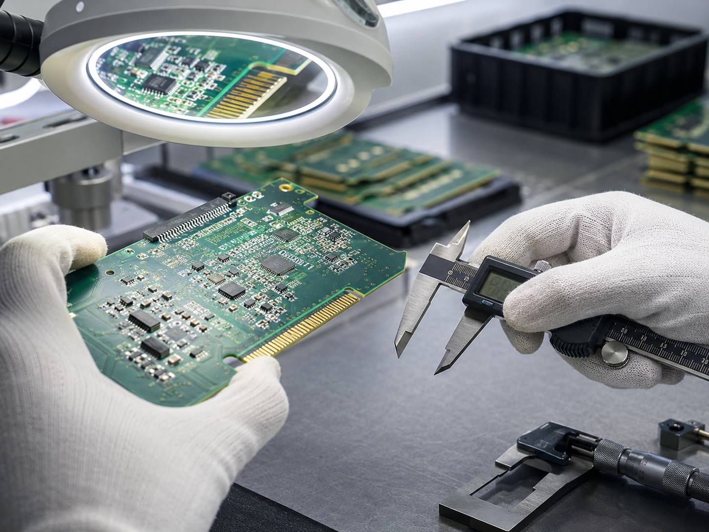
- Routing and final inspection: The PCB is cut to shape by routing, V-cut, or punching. Before shipment or assembly, electrical testing, AOI, dimensional checks, and visual inspection confirm the board meets production requirements.
How Does Commercial PCB Assembly Work After Fabrication?
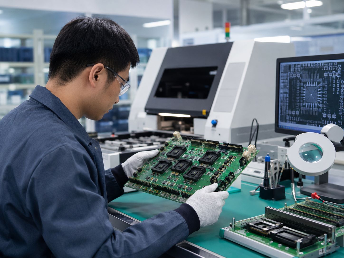
Commercial PCB assembly turns a bare PCB into a functional PCBA by mounting components, soldering them, inspecting solder quality, and testing product performance. This stage directly affects product stability and batch yield.
- Incoming PCB inspection: Bare boards are checked for warpage, oxidation, scratches, solder mask defects, pad problems, and dimensional issues. Poor bare board quality can cause assembly defects later.
- BOM and component check: The BOM is reviewed to confirm part numbers, package sizes, polarity, substitutes, and availability. This reduces wrong-part risk, sourcing delays, and unstable production cost.
- Solder paste printing: Solder paste is printed onto PCB pads through a stencil. Paste volume, stencil opening, and alignment must be controlled because many SMT defects start from poor printing.
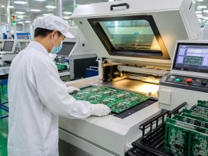
- SMT placement: Pick-and-place machines mount resistors, capacitors, ICs, connectors, LEDs, sensors, and other SMD components. Fine-pitch ICs, BGA, and QFN parts need higher placement accuracy.
- Reflow soldering: The PCB passes through a controlled oven. Solder paste melts and forms solder joints between components and pads. The reflow profile must match board thickness, component type, and solder paste.
- AOI and X-ray inspection: AOI checks missing parts, wrong polarity, skewed parts, solder bridges, and visible solder defects. X-ray is used for BGA, QFN, LGA, and other hidden solder joints.
- Through-hole assembly: Connectors, terminals, relays, switches, transformers, and other through-hole parts are inserted and soldered by wave soldering, selective soldering, or manual soldering.
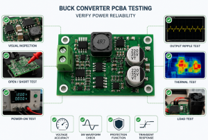
- Cleaning and functional testing: Flux residue, solder balls, and contamination are checked if required. Functional testing verifies power, signal, firmware, buttons, LEDs, sensors, connectors, and other product functions.
- Final inspection and packing: The finished PCBA is inspected, labeled, counted, and packed with ESD protection. Good packing reduces damage during storage and global shipment.
What Is the Difference Between Commercial PCBs and Aerospace PCBs?
Commercial PCBs and aerospace PCBs differ mainly in reliability level, material control, testing depth, documentation, and operating environment. Commercial PCBs are built for stable electronic products, while aerospace PCBs are designed for mission-critical systems under extreme conditions.
| Item | Commercial PCBs | Aerospace PCBs |
|---|---|---|
| Main Goal | Stable function and cost control | Extreme reliability |
| Operating Environment | Normal or moderate conditions | High temperature, vibration, shock, altitude |
| Common IPC Class | Class 2 in many projects | Often Class 3 |
| Material Control | Standard to enhanced | Strict traceability |
| Testing Depth | Electrical, AOI, functional test | Full reliability validation |
| Documentation | Standard production records | Detailed process and material records |
| Cost Level | Controlled | Much higher |
Commercial PCBs are not low-quality boards. They are designed around practical reliability, manufacturability, and cost efficiency. Aerospace PCBs require stricter design rules and validation because a field failure may affect safety-critical systems.
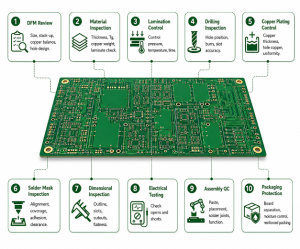
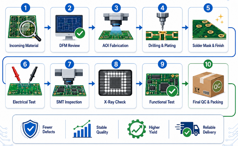
How Do Quality Inspections Improve Commercial PCB Manufacturing Reliability?
Quality inspections improve commercial PCB manufacturing reliability by finding material, fabrication, soldering, and functional problems before the boards reach customers. A good inspection plan checks the PCB from incoming material to final PCBA shipment, instead of relying only on final visual inspection.
- Incoming material inspection: Laminate, copper foil, solder mask, surface finish chemicals, and electronic components should be checked before production. This reduces the risk of poor solderability, unstable insulation, wrong components, or material defects entering commercial PCB manufacturing.
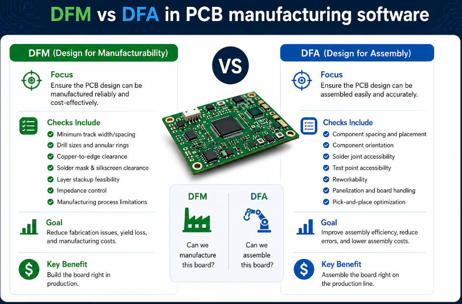
- DFM and file inspection: Gerber files, drill data, stackup, impedance notes, solder mask clearance, and panel design should be reviewed before fabrication. This helps prevent wrong hole sizes, missing layers, weak annular rings, copper spacing problems, and assembly risks.
- AOI during PCB fabrication: Automated Optical Inspection checks inner and outer copper layers for opens, shorts, excess copper, missing copper, and pattern defects. For multi layer commercial PCB production, AOI is important before lamination because hidden inner-layer defects cannot be repaired later.
- Drilling and plating inspection: Hole position, hole size, burrs, hole wall quality, and copper plating thickness should be controlled. Poor drilling or plating can cause via failure, weak electrical connection, intermittent faults, or reliability problems after long-term use.
- Solder mask and surface finish inspection: Solder mask thickness, alignment, pad opening, contamination, oxidation, and finish quality should be checked. Good control improves solderability and reduces solder bridging, exposed copper, poor wetting, and assembly defects.
- Electrical testing for bare boards: Flying probe or fixture testing checks open circuits, short circuits, wrong connections, and netlist problems before assembly. This prevents defective bare boards from entering commercial PCB assembly and wasting components.
- SMT process inspection: SPI checks solder paste volume and alignment before placement. AOI checks missing parts, wrong polarity, skewed components, tombstoning, solder bridges, and visible solder defects after reflow. These inspections improve batch yield and reduce rework.
- X-ray inspection for hidden solder joints: BGA, QFN, LGA, and bottom-terminated components need X-ray inspection because their solder joints cannot be fully seen from the outside. X-ray helps detect voids, bridging, insufficient solder, and hidden connection risks.
- Functional testing after assembly: Functional testing verifies whether the finished PCBA works under real operating conditions. It can check power output, signal communication, firmware, buttons, LEDs, sensors, connectors, and product-specific functions.
- Final quality control and packing inspection: Before shipment, the finished boards should be checked for appearance, labels, quantity, ESD protection, moisture control, and packing strength. Proper final inspection reduces shipping damage, wrong delivery, and customer-side quality complaints.
In commercial PCBs, reliability comes from process control, not one single test. The best inspection plan combines material checks, fabrication inspection, electrical testing, SMT inspection, X-ray when needed, functional testing, and final shipment control.
How Can Commercial PCB Prototypes Move into Stable Batch Production?
Commercial PCB prototypes move into stable batch production when the design, materials, components, test method, and process parameters are verified before scaling. A working prototype does not always mean the product is ready for high volume commercial PCB assembly.
A stable transition usually includes:
- Prototype validation: The first samples are used to check electrical function, dimensions, connectors, mechanical fit, and basic product performance.
- DFM review: The PCB layout is checked for line width, spacing, hole size, solder mask clearance, panel design, and assembly risk.
- BOM review: Components are checked for availability, lifecycle status, package accuracy, substitutes, and long-term sourcing risk.
- Pilot production: A small batch is built to find soldering issues, test problems, fixture needs, and process variation before larger orders.
- Test method locking: Functional tests, inspection standards, firmware loading, and acceptance criteria should be confirmed before batch production.
- Process control: Stencil design, reflow profile, assembly fixture, packing method, and inspection records are locked for repeat orders.
Once the pilot run is stable, the project can move into commercial printed circuit board production with fewer surprises. This approach reduces rework, improves batch yield, and helps buyers control both cost and delivery risk.
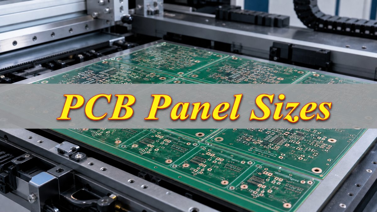
What Factors Affect Commercial PCB Manufacturing Cost and Lead Time?
Commercial PCB manufacturing cost and lead time are mainly affected by board complexity, material selection, surface finish, component availability, test requirements, and order quantity. Simple PCB projects can be produced quickly, while complex PCB and PCBA projects need more engineering control.
| Factor | Cost Impact | Lead Time Impact |
|---|---|---|
| Layer Count | Higher layers increase cost | More lamination time |
| Board Size | Larger panels use more material | May reduce panel efficiency |
| Copper Thickness | More copper raises cost | Longer plating and etching |
| Surface Finish | ENIG costs more than HASL | Extra process control |
| Hole Type | Blind/buried vias cost more | More drilling and plating steps |
| Assembly Density | Fine-pitch parts need precision | Longer SMT setup |
| Components | Shortage parts increase cost | Procurement delays |
| Testing | More tests increase cost | Longer validation cycle |
| Quantity | Higher volume lowers unit cost | More production planning |
Buyers can control cost by confirming final files, clear BOM, approved alternatives, realistic quantity, and required test scope before production begins. Clear project information helps the manufacturer quote more accurately and avoid repeated engineering changes.
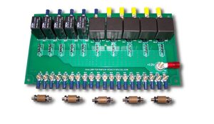
What Services Can We Provide for Commercial PCB Manufacturing and Assembly?
We provide custom commercial PCB solutions from PCB fabrication to PCBA assembly, testing, and batch production support. As a China source factory and global supply manufacturer, EBest Circuit supports overseas buyers with real manufacturing capability and clear engineering communication.
Our commercial PCB services include:
- Commercial PCB fabrication: single-sided, double-sided, multilayer, aluminum, flexible, and rigid-flex PCB.
- Commercial PCB assembly: SMT, THT, mixed assembly, BGA assembly, and fine-pitch component assembly.
- Commercial PCB design services: layout review, DFM checking, stackup advice, and panel optimization.
- Commercial PCB layout services: manufacturability review, pad optimization, routing advice, and production risk reduction.
- Component sourcing: BOM review, approved alternatives, lifecycle checking, and procurement support.
- Testing support: AOI, X-ray, electrical test, functional test, and customized test fixtures.
- Batch production: prototype, pilot run, low-volume production, and high volume commercial PCB assembly.
- Custom support: custom commercial PCB solutions based on product structure, cost target, testing plan, and delivery needs.
This service model helps customers reduce supplier coordination, shorten production communication, and improve batch delivery stability.
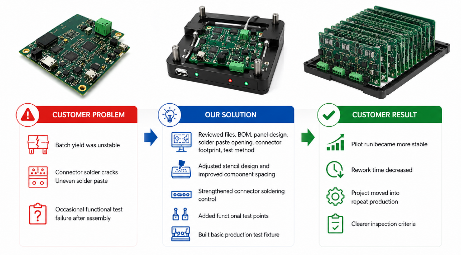
Commercial PCBs Project Case: From Prototype to Stable Batch Production
A smart control device customer needed to move from prototype PCB to stable batch production after facing unstable soldering and inconsistent functional test results. The product used a four-layer FR-4 PCB with SMT components, connectors, and a compact enclosure.
Customer problem: the prototype could power on, but the batch yield was unstable. Several boards showed connector solder cracks, uneven solder paste, and occasional functional test failure after enclosure assembly.
Our solution: EBest Circuit reviewed the Gerber files, BOM, panel design, solder paste opening, connector footprint, and test method. We adjusted the stencil design, improved component spacing, strengthened connector soldering control, added functional test points, and built a basic production test fixture.
Customer result: the pilot run became more stable, rework time decreased, and the project moved into repeat production with clearer inspection criteria. The case shows that commercial PCBs need more than fabrication. They need DFM, assembly control, test planning, and production feedback.
Why Choose EBest Circuit as Your Commercial PCB Manufacturer?
Choose EBest Circuit when you need a commercial PCB manufacturer that can reduce production risk, control cost, and support projects from prototype to batch production. We provide commercial PCB fabrication, commercial PCB assembly, component sourcing, testing, and custom production support as a China source factory serving global customers.
- One-stop PCB and PCBA support: We support PCB fabrication, SMT assembly, THT assembly, BGA assembly, component sourcing, functional testing, and final packing. Customers can manage the full project through one supplier.
- Lower prototype-to-batch risk: We help customers move from commercial PCB prototype fabrication to pilot runs and stable batch production. This helps find design, soldering, BOM, and testing issues before volume production.
- DFM review before production: Our engineering team checks line width, spacing, hole size, solder mask clearance, panel design, and assembly risks. Early review helps reduce redesign, scrap, rework, and delivery delays.
- Material and process advice: We help customers choose suitable FR-4, high-Tg FR-4, aluminum base, copper thickness, and surface finish according to heat, cost, solderability, and product use.
- Strict quality inspection: Commercial PCBs are checked by material inspection, AOI, electrical testing, SPI, X-ray when needed, functional testing, and final inspection. This helps improve batch consistency and reduce field failure risk.
- BOM and sourcing support: We review component package, availability, substitutes, and lifecycle status. This helps reduce purchasing pressure, shortage risk, and unexpected cost changes.
- Flexible order support: Customers can start with prototypes, test a pilot batch, and then move to repeat orders or high volume commercial PCB assembly when the project is stable.
- Global supply from a real China factory: EBest Circuit supports export-ready production, protective packing, clear communication, and global shipment coordination without false overseas factory claims.
FAQs About Commercial PCB Manufacturing and Assembly
Q1: Can commercial PCBs support impedance-controlled designs?
A1: Yes. Commercial PCBs can support impedance control when the project includes high-speed signals, RF circuits, USB, Ethernet, LVDS, HDMI, or antenna-related layouts. The manufacturer needs stackup, trace width, trace spacing, dielectric thickness, and target impedance values before production. Common controlled impedance values include 50Ω single-ended and 90Ω/100Ω differential pairs.
Q2: What PCB thickness is commonly used for commercial PCB boards?
A2: The most common commercial PCB thickness is 1.6mm, but this is not the only option. Compact products may use thinner boards such as 0.8mm or 1.0mm, while power boards, connectors, or mechanically stressed products may need thicker boards. Thickness should match enclosure space, connector height, strength, and assembly requirements.
Q3: What copper thickness is suitable for commercial PCBs?
A3: Many commercial PCBs use 1oz copper, which is suitable for general signal and low-power circuits. Higher current products may need 2oz or heavier copper to reduce heat and voltage drop. Copper thickness should be selected based on current load, trace width, temperature rise, board space, and cost target.
Q4: Can commercial PCBs be made with lead-free materials?
A4: Yes. Most export-oriented commercial PCBs can be produced with lead-free surface finishes and RoHS-compliant materials. Common lead-free finishes include ENIG, OSP, immersion silver, and lead-free HASL. For overseas buyers, RoHS compliance is often important for consumer electronics, lighting products, communication devices, and general commercial equipment.
Q5: How long can bare commercial PCB boards be stored before assembly?
A5: Storage life depends on surface finish, packaging, humidity, and storage temperature. ENIG usually offers better shelf life than OSP, while OSP should be assembled sooner to avoid solderability loss. Bare boards should be stored in dry, sealed packaging. Moisture, oxidation, and handling contamination are the main risks during storage.
Q6: Do commercial PCBs need UL marking?
A6: UL marking may be required when the final product, customer market, or safety certification demands it. It is common in power products, lighting, industrial control, and export electronics. The PCB material and factory process must match the approved UL file. Buyers should confirm UL requirements before production, not after the boards are finished.
Q7: Can the solder mask color affect commercial PCB production?
A7: Yes, but the effect is usually small for standard colors. Green solder mask is the most common and stable choice. Black, white, blue, red, and matte colors may require more attention during inspection because contrast, surface appearance, or light reflection can affect AOI and visual checking. Green is often preferred for easier inspection and stable production.
Q8: What causes solder joint cracks in commercial PCB assembly?
A8: Solder joint cracks may come from poor pad design, insufficient solder, heavy connectors, thermal stress, vibration, board bending, or weak mechanical support. Large connectors, terminals, relays, and switches need stronger footprint design and proper soldering control. For products with mechanical stress, fixture support and connector reinforcement can reduce cracking risk.
Q9: Can commercial PCBs support firmware programming after assembly?
A9: Yes. Firmware programming can be arranged after PCBA assembly if the board includes proper programming ports, test pads, connectors, or fixtures. Buyers should provide firmware files, programming tools, instructions, and verification methods. Programming should be planned during design, because missing access points can make batch programming slow or difficult.
Q10: What should buyers check before approving the first assembled sample?
A10: Buyers should check electrical function, connector fit, enclosure fit, polarity, LED direction, firmware behavior, communication ports, temperature rise, mechanical strength, and test results. A first sample should not be approved only because it powers on. Approval should confirm both function and manufacturability before moving to batch production.
Q11: Can commercial PCBs be packed for long-distance international shipping?
A11: Yes. Commercial PCBs and assembled PCBAs can be packed with ESD bags, vacuum packaging, moisture barrier bags, trays, foam, cartons, and labels based on product sensitivity. For assembled boards with ICs, displays, connectors, or fragile parts, stronger protection is recommended. Good export packing reduces moisture, static damage, and transport deformation.
Q12: How can buyers protect design confidentiality when ordering commercial PCBs?
A12: Buyers can use NDA agreements, controlled file sharing, limited document access, and clear project authorization. The manufacturer should only use design files for quoting, engineering review, production, testing, and delivery. For sensitive projects, buyers can also separate firmware, enclosure files, or key design data. Clear confidentiality rules help protect custom commercial PCB solutions.
Conclusion
Commercial PCBs should be designed, fabricated, assembled, and tested around real product use, batch stability, and cost control. The best result comes from clear files, suitable materials, reliable assembly, and practical inspection standards.
EBest Circuit supports commercial PCB fabrication, commercial PCB assembly, prototype builds, and batch production as a China source factory serving global customers. Send your Gerber files, BOM, quantity, and testing requirements to sales@bestpcbs.com for a fast quote.