PCB thickness tolerance is one of the most important mechanical requirements in PCB manufacturing. It affects enclosure fit, connector alignment, controlled impedance, heat transfer, assembly stability, and final product reliability. For many engineers, the key question is simple: if the design calls for a 1.6mm FR4 PCB, how close will the finished board be to that number after lamination, copper plating, solder mask, surface finish, and final inspection?
EBest Circuit (Best Technology) supports custom PCB and PCBA projects where finished PCB thickness tolerance must match real product requirements, such as connector fit, housing assembly, impedance control, and prototype-to-production consistency. Our engineering team can review your stackup, material, copper thickness, mechanical drawing, and tolerance notes before production, so board thickness risks are not discovered too late. If you are working on a PCB project with strict thickness requirements, pls feel free to send your Gerber files, stackup, drawings, or questions to sales@bestpcbs.com. We will help you check the practical manufacturing path before the board is built.
What Is PCB Thickness Tolerance?
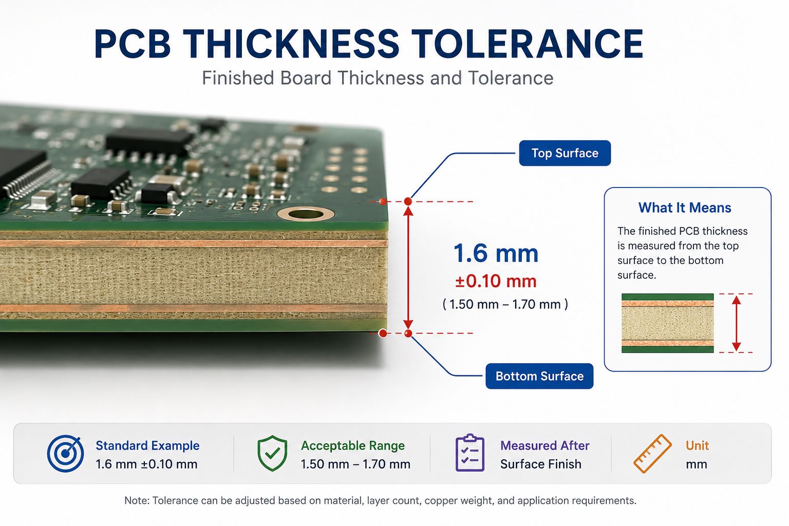
PCB thickness tolerance is the allowed variation between the designed board thickness and the actual finished board thickness after manufacturing.
For example, if a PCB is specified as 1.6mm thick with a +/-10% tolerance, the finished PCB thickness may be acceptable within a range of about 1.44mm to 1.76mm. If the project requires a tighter mechanical fit, the drawing may specify a narrower tolerance such as +/-0.10mm, but the feasibility depends on the material, stackup, copper weight, and production process.
PCB thickness tolerance is not only a number on a drawing. It can affect:
- Connector fit and insertion depth
- Card-edge contact reliability
- Enclosure and screw-hole alignment
- Controlled impedance stackup
- Thermal performance
- Mechanical stiffness
- Assembly yield
- Product appearance
For simple prototype boards, standard tolerance may be enough. For products with slots, housings, camera modules, medical electronics, automotive modules, or high-speed interfaces, thickness tolerance should be reviewed before production.
FR4 PCB Thickness Tolerance in Manufacturing
FR4 PCB thickness tolerance is the thickness variation of a finished PCB made with FR4 laminate and prepreg. FR4 is the most common PCB base material, but it is not perfectly fixed in thickness. Laminate suppliers, copper foil, resin content, press conditions, and final surface finish can all create variation.
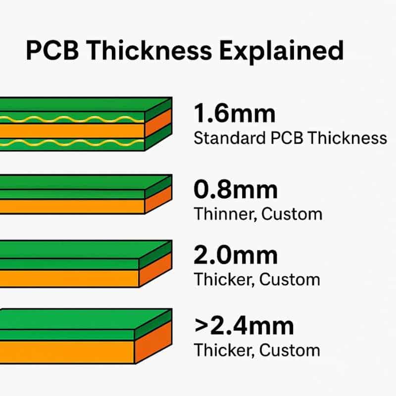
Common FR4 PCB thicknesses include 0.4mm, 0.6mm, 0.8mm, 1.0mm, 1.2mm, 1.6mm, 2.0mm, and 2.4mm. Among these, 1.6mm is the most widely used standard thickness for many rigid PCB applications.
In many standard FR4 PCB manufacturing projects, +/-10% is often treated as a practical reference range. However, this should not be assumed for every board. Thin boards, heavy copper boards, multilayer boards, impedance-controlled boards, and boards that must fit into a precise enclosure may need a different tolerance agreement.
At EBest Circuit, FR4 PCB thickness is reviewed together with the stackup, copper weight, board size, panel arrangement, surface finish, and assembly requirements. This matters because the board the customer receives is the finished PCB, not only the raw laminate.
PCB Board Thickness Tolerance Before and After Production
PCB board thickness tolerance should be considered in two stages: the designed thickness before production and the finished thickness after production.
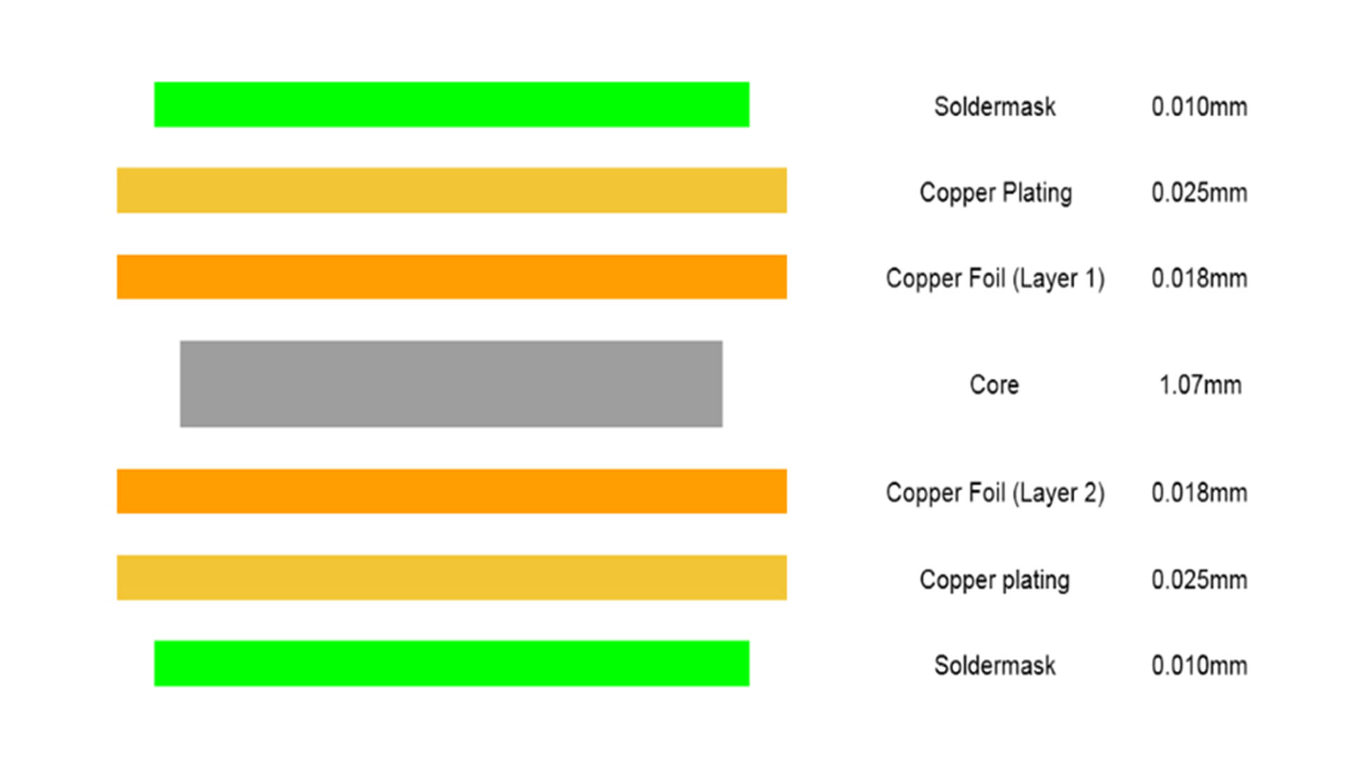
Before production, the drawing or stackup may define the target board thickness. This can include the core, prepreg, copper layers, and sometimes solder mask or surface finish assumptions. For many products, the target thickness is selected based on standard material availability and mechanical requirements.
After production, the final board thickness can be affected by several process factors:
| Factor | Effect |
|---|---|
| Core | Base thickness variation |
| Prepreg | Resin flow after pressing |
| Copper | Adds stackup height |
| Lamination | Changes dielectric thickness |
| Finish | Small final surface change |
This is why a PCB drawing should clearly state whether the thickness tolerance refers to the finished PCB thickness. If the requirement is only written as “1.6mm PCB” without tolerance, the manufacturer may quote a standard tolerance instead of a tighter one.
Finished PCB Thickness Tolerance and Why It Matters
Finished PCB thickness tolerance refers to the final measured board thickness after all major PCB processes are complete. This is the value that matters most for product assembly.
Finished PCB thickness is especially important when the PCB must connect with:
- Edge-card connectors
- FPC or board-to-board connectors
- Mechanical slots
- Press-fit parts
- Screw bosses or plastic housings
- Heat sinks or thermal pads
- Optical or sensor modules
- Shielding cans
If the finished board is too thick, it may not fit the enclosure or connector. If it is too thin, connector contact pressure, stiffness, or vibration resistance may be affected. In high-speed boards, a change in dielectric thickness can also affect impedance.
For this reason, engineering drawings should define the finished PCB thickness tolerance clearly. A good note may include:
Finished PCB thickness: 1.6mm +/-0.10mm, measured after surface finish.
If the tolerance is critical, the manufacturer should review feasibility before production and confirm whether special material selection, stackup control, or process control is needed.
PCB Thickness Tolerance IPC Standards
Many engineers search for PCB thickness tolerance IPC standards because they want a reliable reference. IPC standards are important in PCB manufacturing, but it is risky to assume that one universal IPC number applies to every PCB thickness tolerance case.
IPC documents such as IPC-6012 and IPC-A-600 are commonly used for rigid PCB performance and acceptability requirements. They help define quality expectations, inspection criteria, and acceptance conditions. However, for board thickness, the customer’s drawing, procurement specification, stackup, material selection, and manufacturer capability are still very important.
In practical PCB manufacturing, the safest approach is:
- Define the target finished PCB thickness.
- Define the acceptable tolerance.
- Confirm whether the tolerance applies before or after surface finish.
- Confirm whether thickness is measured at panel level or finished board level.
- Ask the PCB manufacturer to review stackup feasibility.
If your project requires IPC Class 2 or Class 3 production, mention it clearly. If your product is used in medical, automotive, aerospace, industrial control, or high-reliability electronics, the thickness tolerance should be part of the full DFM and quality review, not a small note at the end of the drawing.
1.6mm PCB Thickness Tolerance and 62 Mil Boards
The most common PCB thickness is 1.6mm, often also called about 62 mil or 63 mil. The exact conversion is close, but in everyday PCB sourcing, engineers often use 1.6mm and 62 mil as practical equivalents.
A standard 1.6mm FR4 PCB is widely used because it offers a good balance of stiffness, availability, cost, and assembly compatibility. Many manufacturers can support a standard tolerance such as +/-10%, but this may be too wide for products that depend on connector fit, housing slots, card-edge contacts, or precise mechanical positioning.
Engineers may also compare 1.6t vs 1.2 PCB when choosing board thickness. In this context, 1.6t usually means a 1.6mm thick PCB, while 1.2 PCB usually means a 1.2mm thick board. A 1.6mm board is generally stiffer and more common for standard FR4 assemblies, while a 1.2mm board can help reduce product thickness or weight. However, the final choice should depend on enclosure space, connector requirements, mechanical strength, stackup, and the finished PCB thickness tolerance.
For example:
| Requirement | Why It Matters |
|---|---|
| 1.6mm +/-10% | Common for standard FR4 boards |
| 1.6mm +/-0.15mm | Better for mechanical fit |
| 1.6mm +/-0.10mm | Needs tighter stackup review |
| 1.2mm PCB | Useful for thinner products |
| 62 mil card-edge PCB | Connector fit should be confirmed |
If your product uses a card-edge connector, do not only write “1.6mm PCB”. Confirm the connector datasheet and define the required finished board thickness at the contact area. In some cases, plating, beveling, surface finish, and edge tolerance may also need attention.
Core, Prepreg, and Dielectric Thickness Tolerance in PCBs
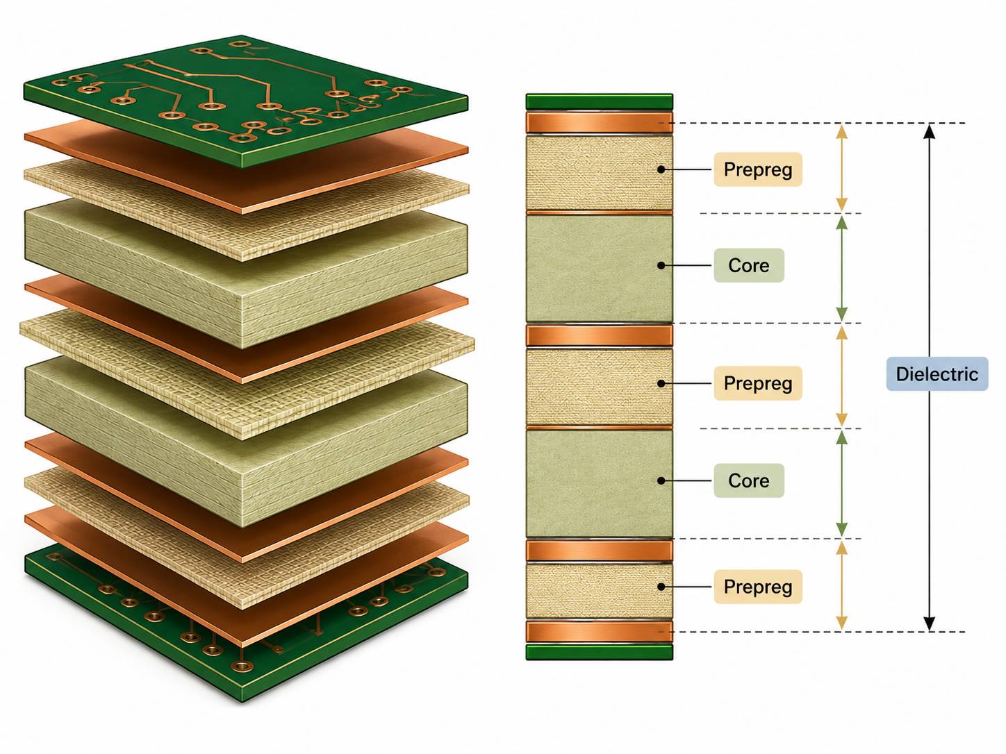
PCB thickness tolerance is built from several material layers. For multilayer boards, the final thickness is not only one piece of FR4. It is the result of cores, prepregs, copper layers, lamination, and final processing.
The three key terms are:
| Term | Meaning |
|---|---|
| PCB core thickness tolerance | Variation in the rigid core material |
| PCB prepreg thickness tolerance | Variation after prepreg resin flows during lamination |
| PCB dielectric thickness tolerance | Variation in insulation thickness between copper layers |
Dielectric thickness matters because it affects impedance. If a high-speed design requires 50-ohm single-ended impedance or 90/100-ohm differential impedance, the dielectric thickness cannot be treated casually.
For controlled impedance boards, engineers should provide:
- Gerber files
- Stackup requirement
- Copper thickness
- Impedance target
- Reference layers
- Trace width and spacing
- Test coupon requirement
- Impedance test report requirement
EBest Circuit reviews these details during DFM before production. If the required impedance and the requested finished PCB thickness conflict, the stackup may need adjustment before manufacturing begins.
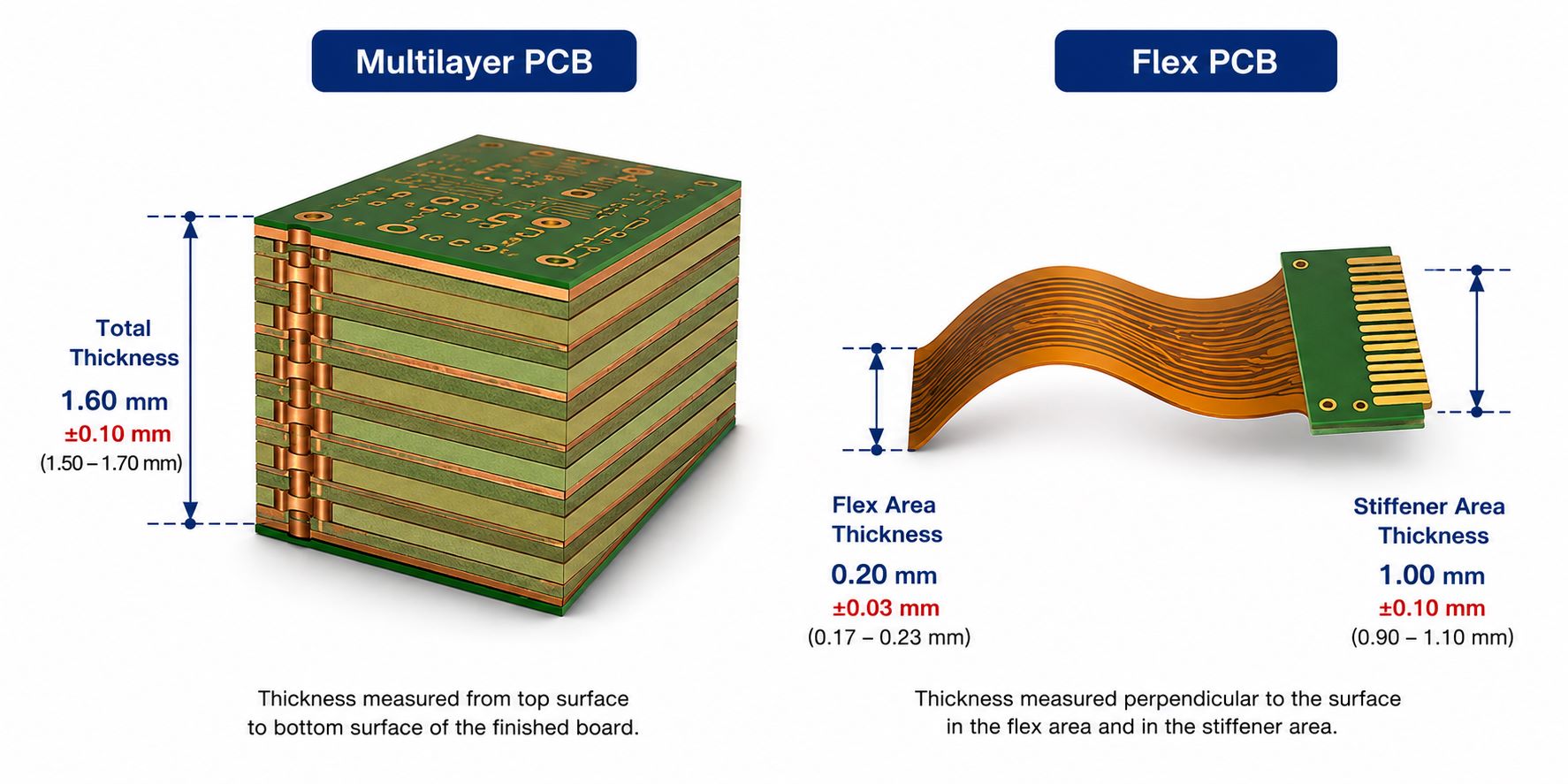
Multilayer and Flex PCB Thickness Tolerance
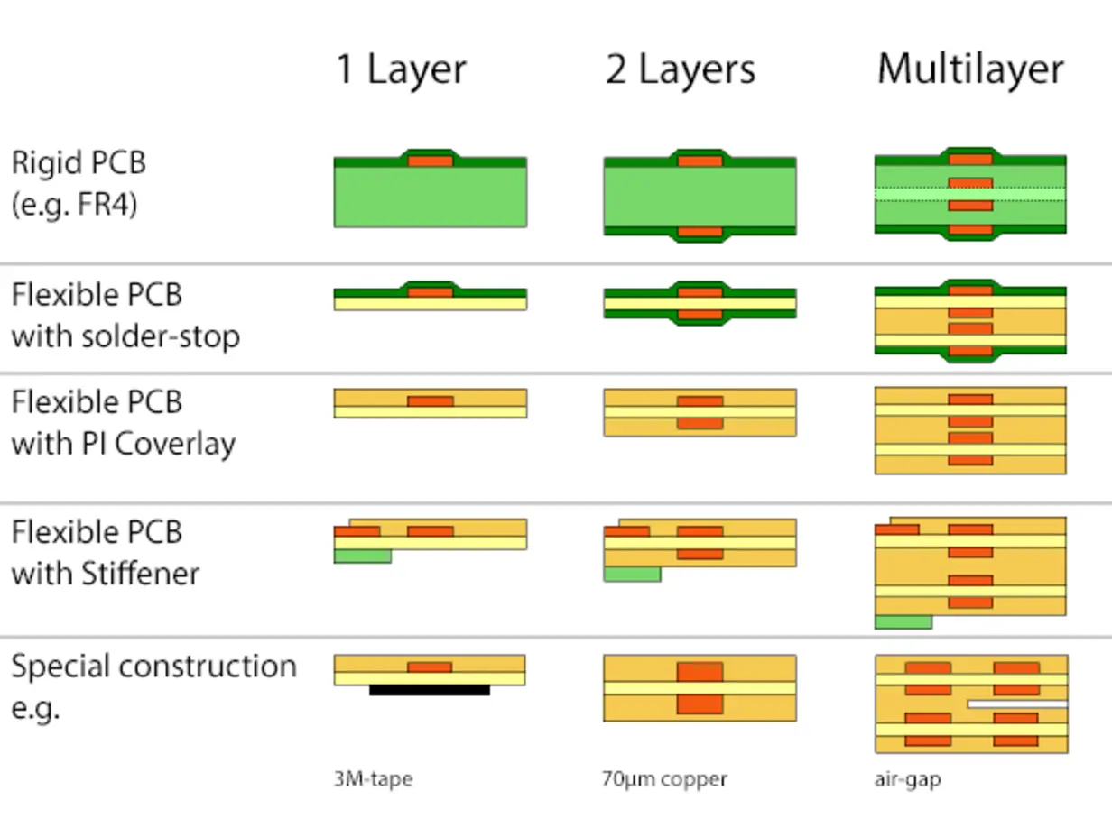
Multi-layer PCB thickness tolerance is usually more complex than simple double sided pcb boards. More layers mean more cores, prepregs, copper layers, and lamination variables. A 4-layer, 6-layer, 8-layer, or 10-layer board may require a custom stackup instead of a standard laminate.
For multilayer boards, thickness tolerance affects:
- Controlled impedance
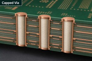
- Via aspect ratio
- Lamination stability
- Warpage risk
- Press-fit and connector fit
- Mechanical strength
- Thermal path
Flex PCB thickness tolerance is different again. Flexible PCB thickness may include PI film, adhesive, copper foil, coverlay, stiffener, shielding film, and surface finish. A flex PCB may be extremely thin, but connector-end thickness may be built up with FR4 or PI stiffeners.
When comparing multilayer PCB thickness tolerance and flex PCB thickness tolerance, the key question is not only “how thick is the PCB?” It is also:
- Where is the thickness measured?
- Is the stiffener included?
- Is the connector end thicker than the flexible area?
- Is the board rigid, flex, or rigid-flex?
- Does the finished product need bending?
For flex and rigid-flex projects, always provide the mechanical drawing. A simple Gerber file is usually not enough to control thickness correctly.
How to Choose a PCB Manufacturer for Tight Board Thickness Tolerance
If your project needs tight board thickness tolerance, choose a PCB manufacturer that can review the requirement before quoting, not only after production begins.
A reliable PCB manufacturer should be able to check:
- Target finished PCB thickness
- FR4 material and laminate availability
- Stackup feasibility
- Core and prepreg selection
- Copper thickness and plating impact
- Impedance requirements
- Connector or enclosure fit
- Warpage and mechanical risk
- Measurement and inspection method
- Prototype and production consistency
For high tolerance board thickness projects, communication is as important as manufacturing capability. A small mismatch in drawing notes can lead to a board that is electrically acceptable but mechanically unsuitable.
EBest Circuit supports quick PCB fabrication, component sourcing, PCB SMT assembly, DFM review, BOM optimization, testing, and small-batch or mass production. Our engineering team helps customers check board thickness tolerance together with real product requirements, including enclosure fit, connector requirements, impedance control, and assembly process.
For projects where thickness matters, we recommend sending the Gerber files, stackup, mechanical drawing, connector datasheet, and any finished thickness tolerance requirement before production. This helps prevent rework and shortens the path from prototype to reliable production.
FAQs about PCB Thickness Tolerance
What does PCB dimension tolerance IPC mean?
PCB dimension tolerance IPC usually refers to dimensional quality expectations guided by IPC standards and project drawings. For thickness, outline, holes, and slots, the safest method is to define the exact tolerance on the drawing and ask the PCB manufacturer to confirm feasibility before production.
What is PCB board outline tolerance?
PCB board outline tolerance is the allowed variation in the finished board shape, length, width, or routed edge. It matters when the PCB must fit into an enclosure, slot, camera housing, connector frame, or mechanical fixture.
Is PCB trace width tolerance related to PCB thickness tolerance?
PCB trace width tolerance is not the same as board thickness tolerance, but both can affect impedance. For controlled impedance PCBs, trace width, dielectric thickness, copper thickness, and stackup should be reviewed together.
Why do PCB hole position tolerance and PTH tolerance matter?
PCB hole position tolerance affects how well mounting holes, vias, and connectors align with the product. PCB PTH tolerance affects plated through-hole fit, solderability, and component insertion. Both should be controlled when the PCB has tight mechanical or assembly requirements.
How much PCB board edge clearance should I keep?
PCB board edge clearance depends on routing, copper spacing, voltage, connector location, and enclosure design. As a general rule, keep critical copper, holes, and components away from the routed edge and confirm the clearance with your PCB manufacturer during DFM review.
If you need help with PCB thickness tolerance, FR4 PCB thickness tolerance, 1.6mm PCB tolerance, or a mechanically sensitive PCB project, pls feel free to send your Gerber files, stackup, drawings, and project notes to sales@bestpcbs.com. EBest Circuit can help review your files and recommend a practical manufacturing path before production starts.