Multi layer printed circuit board technology helps engineers place more circuitry, power distribution, signal routing, and ground shielding inside a compact board structure. Compared with a single layer or double-sided PCB, a multilayer PCB gives the designer more routing layers, better electrical control, and more space for complex electronics.
EBest Circuit (Best Technology) supports custom multilayer PCB manufacturing with DFM review, engineering response, material and process review, PCB fabrication, component sourcing, PCBA assembly, testing, and shipment documentation. A warm welcome to send your Gerber files, stack-up notes, quantity, and delivery requirements to sales@bestpcbs.com for an engineering review.
What Is a Multi Layer Printed Circuit Board?
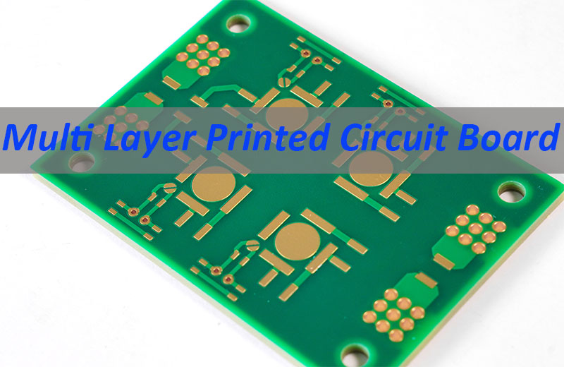
A multi layer printed circuit board is a PCB made with three or more conductive copper layers laminated together with insulating material. In practical PCB manufacturing, multilayer boards usually start from 4 layers and can increase to 6, 8, 10, 12 layers or more depending on the design.
Each conductive layer can be used for signal routing, power distribution, ground reference, shielding, or controlled impedance structures. The layers are connected by plated through holes, blind vias, buried vias, or other via structures depending on the design requirement.
Multilayer PCBs are widely used in:
- Industrial control systems
- Communication equipment
- Power electronics
- Medical devices
- Automotive electronics
- Aerospace and defense electronics
- Data processing and computing hardware
- IoT and compact smart devices
- High-speed and high-density electronics
The purpose of a multilayer PCB is not simply to make the board look more advanced. It is used when the circuit needs better routing density, cleaner power and ground structure, improved signal integrity, higher reliability, or a smaller product size.
How Multi-Layer Printed Circuit Boards Are Built
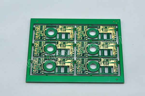
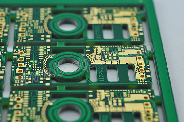
Multi-layer printed circuit boards are built by combining copper foil, prepreg, and core material into a laminated structure. The internal circuit layers are imaged, etched, inspected, and then pressed together under heat and pressure. After lamination, the board goes through drilling, copper deposition, electroplating, outer layer imaging, solder mask, silkscreen, surface finish, profiling, electrical testing, final inspection, and shipment.
Based on the manufacturing process material, a simplified multilayer PCB flow includes:
- Material preparation and panel cutting
- Inner layer imaging
- Inner layer etching
- Inner layer AOI inspection
- Brown oxide or surface roughening before lamination
- Lay-up with core, prepreg, and copper foil
- Lamination under heat and pressure
- Drilling
- Desmear and electroless copper
- Copper plating
- Outer layer imaging and etching
- Outer layer AOI
- Solder mask
- Silkscreen
- Surface finish such as ENIG, HASL, OSP, immersion tin, or immersion silver
- Routing, V-cut, countersink, counterbore, or other mechanical processing
- Electrical test
- Final quality inspection
- Packing and shipment report
For buyers, this process explains why a multilayer PCB needs more engineering review than a simple board. If the stack-up, drill structure, copper thickness, or documentation is unclear, production questions can delay the order before fabrication even starts.
Multi Layer Printed Circuit Board Stack-Up Basics
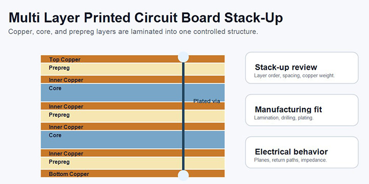
The stack-up is the internal structure of a multi layer printed circuit board. It defines the number of copper layers, dielectric thickness, core thickness, prepreg selection, copper weight, finished board thickness, and the relationship between signal, power, and ground layers.
In a typical multilayer structure, the main materials include:
- Copper foil: Conductive material used for circuit layers.
- Core: A cured laminate with copper on one or both sides.
- Prepreg: A partially cured resin and glass fiber material used to bond layers during lamination.
- Solder mask: Protective coating applied to the outer board surface.
- Surface finish: Metal or organic finish applied to exposed pads for solderability and protection.
The stack-up affects more than thickness. It influences impedance, warpage, lamination yield, copper balance, drilling quality, heat dissipation, and long-term reliability.
For high-density or high-speed boards, stack-up review is especially important because signal layers often need a nearby ground plane. For heavy copper boards, stack-up planning is also critical because copper distribution, resin flow, dielectric spacing, and lamination pressure can affect manufacturability.
Before production, buyers should confirm:
- Final layer count
- Finished board thickness and tolerance
- Inner and outer copper thickness
- Dielectric spacing
- Controlled impedance needs
- Material brand or equivalent options
- Surface finish
- Via structure
- Special mechanical requirements
- Testing and documentation requirements
Multi Layer Printed Circuit Board vs Single Layer PCB: Key Differences
A single layer PCB has one conductive copper layer. It is usually suitable for simple circuits, low-cost electronics, LED products, basic power boards, and simple consumer devices.
A multi layer printed circuit board has multiple copper layers laminated into one board. It is used when the design needs higher routing density, better power distribution, improved signal control, compact size, or stronger electrical performance.
Key differences include:
- Circuit density: Multilayer PCBs support more routing in limited space.
- Electrical performance: Ground and power planes can improve noise control and signal reference.
- Mechanical complexity: Multilayer boards require lamination, registration control, and more inspection.
- Cost: Multilayer PCBs cost more because of extra material, process steps, and engineering control.
- Lead time: Multilayer production usually takes longer than single layer or double-sided boards.
- Application level: Multilayer boards are more common in industrial, medical, communication, automotive, and high-performance electronics.
If a product only needs simple electrical connection, a single layer or double-sided PCB may be enough. If the product requires high density, lower noise, better power integrity, smaller size, or complex interconnection, a multilayer board is often the better choice.
Benefits of Multi-Layer Printed Circuit Boards for Compact Electronics
Multi-layer printed circuit boards are widely used because modern electronics need more functions inside smaller products. A multilayer PCB allows engineers to place power, ground, signal, and control circuits in a more organized structure.
Main benefits include:
- Higher routing density: More copper layers allow more traces without increasing board area.
- Smaller product size: Complex circuits can fit into compact enclosures.
- Better signal integrity: Ground planes and controlled layer spacing can reduce noise and improve signal behavior.
- Improved power distribution: Dedicated power and ground planes support stable current flow.
- Stronger EMI control: Internal planes can help shield sensitive signals.
- Support for high-speed design: Layer planning can support impedance and return paths.
- Better product integration: More functions can be combined on one board.
For compact electronics, the advantage is not only space saving. A good multilayer structure can also make the product easier to test, assemble, and scale into production.
Layout Tips for High Density Multi-Layer PCBs
High density multi-layer PCB layout should be planned with manufacturing, assembly, and signal behavior in mind. A layout may pass software checks but still create problems in fabrication or assembly if spacing, vias, copper balance, and documentation are not reviewed.
Important layout tips include:
- Keep critical signals close to a continuous reference plane.
- Avoid unnecessary breaks in the return path.
- Confirm impedance requirements before routing high-speed traces.
- Keep differential pairs consistent in spacing and length where required.
- Plan via type and via size based on manufacturability.
- Avoid placing dense vias too close to pads unless via-in-pad is intended and supported.
- Balance copper distribution to reduce warpage risk.
- Leave enough solder mask clearance for fine-pitch components.
- Confirm annular ring, drill-to-copper clearance, and edge clearance.
- Separate high-current paths from sensitive signal areas.
- Clearly mark special requirements in the fabrication notes.
EBest Circuit can support PCB layout-related manufacturability review and DFM feedback. For work beyond PCB layout, such as full circuit design, electrical architecture, or product-level design decisions, the customer engineering team should provide the design intent and requirements.
Materials for Heat Resistant Multi-Layer PCBs
A heat resistant multi-layer printed circuit board needs material and structure choices that match the working temperature, assembly temperature, current load, and reliability requirement.
Common material factors include:
- Tg value: The glass transition temperature indicates when the resin system begins to soften. Higher Tg material may be needed for higher thermal stress.
- CTE behavior: Lower and more stable expansion helps reduce stress on plated holes and internal connections.
- Copper thickness: Heavy copper can support higher current, but it also increases manufacturing difficulty.
- Board thickness: Thicker boards may improve mechanical strength but can make drilling and plating more demanding.
- Surface finish: ENIG is often selected when good solderability, flat pads, and storage stability are needed.
- Thermal design: Copper planes, trace width, spacing, and component placement affect heat spreading.
FR4 can be suitable for many multilayer boards, but not every FR4 material is the same. For high-temperature, high-current, high-reliability, or high-speed products, the material brand, Tg, dielectric properties, copper thickness, and lamination structure should be reviewed before production.
Multi-Layer PCB Manufacturing Time and Cost
Multi-layer PCB manufacturing time and cost are affected by more than layer count. Two 12-layer boards can have very different cost and lead time if one is a standard signal board and the other is a heavy copper, thick board with special mechanical holes and full documentation.
Key factors include:
- Layer count
- Board size and panel utilization
- Material brand and availability
- Inner and outer copper thickness
- Finished board thickness
- Minimum trace and spacing
- Drill count and drill size
- Via structure
- Controlled impedance
- Surface finish
- Solder mask and silkscreen requirements
- Countersink, counterbore, slots, or special routing
- Electrical test requirements
- Reports, COC, dimensional report, impedance report, or shipment report
Speedy delivery does not mean skipping engineering review. For multilayer PCBs, the fastest schedule usually comes from complete files, fast engineering confirmation, available material, clear stack-up, and early agreement on testing and documentation.
To reduce avoidable delay, buyers should send:
- Gerber files or ODB++ files
- Drill files
- Stack-up drawing
- Material requirements
- Copper thickness
- Finished board thickness and tolerance
- Surface finish
- Quantity
- Delivery deadline
- Electrical test and report requirements
- Special notes for countersink, counterbore, slots, controlled impedance, or packaging
Case Study: Custom 12-Layer Heavy Copper Multi Layer Printed Circuit Board
A German industrial power equipment customer needed a 12-layer heavy copper PCB for a high-current control module. The board had to support current carrying capability, stable mechanical assembly, and final electrical verification before shipment.
The main specifications were:
- 12-layer PCB with ISOLA FR4
- 5 oz inner copper and 6 oz finished outer copper
- 4.394 mm +/-10% finished board thickness
- Green solder mask, white silkscreen, ENIG
- Countersink and counterbore holes
- 100% electrical test with shipment report
This project was not difficult because of layer count alone. The real challenge was the combination of 12 layers, heavy copper, thick board construction, ENIG, and mechanical hole requirements. Heavy copper affects etching, resin filling, lamination, drilling, plating, solder mask coverage, and final thickness control. Countersink and counterbore holes also had to match the customer’s assembly method, not just the PCB drawing.
Before production, the engineering review focused on four practical points:
- Whether the heavy copper stack-up could meet the finished thickness tolerance.
- Whether spacing, drilling, and plating were suitable for a thick 12-layer structure.
- Whether countersink and counterbore details were clear enough for assembly use.
- Whether 100% electrical test and shipment reporting could be completed before delivery.
For this type of custom multi layer printed circuit board, speedy delivery depends on early technical confirmation. Once the stack-up, material, mechanical holes, and testing documents are confirmed, production can move faster with fewer late-stage questions.
Why Choose EBest Circuit as a Custom Multi Layer Printed Circuit Board Manufacturer?
EBest Circuit (Best Technology) is a custom PCB and PCBA manufacturer supporting global buyers with PCB fabrication, component sourcing, PCBA assembly, testing, DFM review, BOM optimization, and engineering support.
For custom multi layer printed circuit board projects, EBest Circuit is suitable when buyers need:
- Engineering response before production
- DFM review for manufacturability risks
- Stack-up and process discussion
- Multilayer PCB manufacturing
- Heavy copper, impedance, special material, metal core, ceramic, HDI, high-frequency, or other customized PCB support
- PCB manufacturing and PCBA assembly from one supplier
- Component sourcing and BOM optimization
- Sample and small-batch support
- Quality documentation and shipment reports
- Traceable production progress
- Faster delivery planning for suitable projects
EBest Circuit’s service model combines one sales contact with engineering support throughout the project. This helps customers avoid fragmented communication between quotation, engineering review, manufacturing, assembly, and shipment.
The company was founded in 2006 and has experience supporting global engineers and electronics companies across prototype, sample, small-batch, and production stages. Certifications and quality support include ISO 9001, ISO 13485, IATF 16949, AS9100D, REACH, RoHS, and UL-related quality support.
For buyers, the main value is not only that EBest Circuit can manufacture multilayer PCBs. The value is that the project can be reviewed before production, manufacturing questions can be clarified early, and PCB fabrication, sourcing, assembly, testing, and documentation can be coordinated under one supplier when needed.
FAQs about Multi Layer Printed Circuit Board
What is a multi layer printed circuit board?
A multi layer printed circuit board is a PCB with three or more conductive copper layers laminated together with insulating materials. It is commonly used when the product needs higher routing density, better signal control, smaller size, or more reliable power and ground distribution.
How many layers can a multilayer PCB have?
Common multilayer PCBs include 4-layer, 6-layer, 8-layer, 10-layer, and 12-layer boards. Higher layer counts are possible, but cost, lead time, material selection, lamination control, and testing requirements increase as the design becomes more complex.
Why are multilayer PCBs more expensive than single layer PCBs?
Multilayer PCBs require more material, inner layer imaging, lamination, drilling, plating, inspection, and engineering control. Stack-up complexity, copper thickness, controlled impedance, special materials, and documentation requirements can also increase cost.
What affects the lead time of a custom multi layer printed circuit board?
Lead time is affected by layer count, material availability, copper thickness, board thickness, hole structure, minimum line and spacing, surface finish, mechanical processing, electrical test, inspection, and required reports. Complete files and fast engineering confirmation can help shorten the schedule.
Can EBest Circuit support heavy copper multilayer PCB projects?
Yes. EBest Circuit can review heavy copper multilayer PCB projects and provide manufacturability feedback before production. For boards with thick copper, special materials, controlled thickness, countersink holes, counterbore holes, or testing reports, buyers should send complete fabrication notes and drawings for engineering review.
Does EBest Circuit provide PCB layout support?
EBest Circuit can support PCB layout-related review and manufacturability feedback. Full circuit design or product-level electronic design beyond PCB layout should be provided or confirmed by the customer’s engineering team.
All in all, a multi layer printed circuit board is not only a board with more layers. It is a manufacturing structure that must balance routing density, material selection, lamination quality, copper thickness, drilling, plating, solderability, testing, and delivery planning.
If you need a custom multi layer printed circuit board manufacturer with engineering support and practical delivery planning, EBest Circuit (Best Technology) can review your Gerber files, stack-up, material requirements, copper thickness, quantity, and testing documents before production. Send your project files to sales@bestpcbs.com for an engineering review.