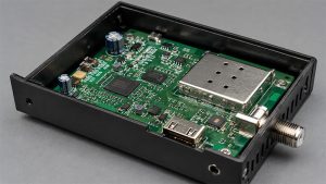
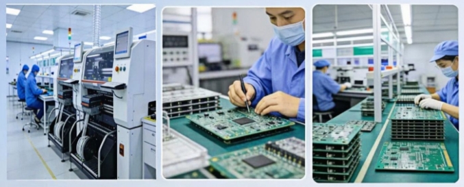
An intercom circuit board integrates voice capture, audio processing, wired or wireless communication, power management and access-control functions. Reliable operation depends on circuit architecture, PCB layout, component quality, firmware and production testing. EBest Circuit provides custom PCB manufacturing and assembly services for door-entry systems, wireless intercoms, building communication panels and industrial talkback equipment.
Are you worried about these problems in intercom circuit board projects?
- Design challenges: Poor grounding, incorrect gain settings or unsuitable antenna placement may cause noise, echo, weak audio and unstable wireless communication.
- Production risks: Incomplete files, material shortages and uncontrolled impedance may delay prototypes or affect batch consistency.
- Assembly difficulties: Fine-pitch parts, microphones, wireless modules and hidden solder joints require precise placement and reliable inspection.
As a one-stop PCBA service provider with more than 20 years of industry experience, EBest Circuit provides the following solutions:
- Design optimization: We review audio circuits, power distribution, grounding, RF routing and antenna layout to reduce noise and communication failures.
- Controlled production: We verify manufacturing files, materials, impedance and component availability before fabrication to reduce delays and redesigns.
- Reliable assembly and testing: We provide SMT and THT assembly, SPI, AOI, X-ray, programming and functional testing to verify product performance.
Send your Gerber files, BOM and test requirements to EBest Circuit via sales@bestpcbs.com for a quotation.
What Is an Intercom Circuit Board?
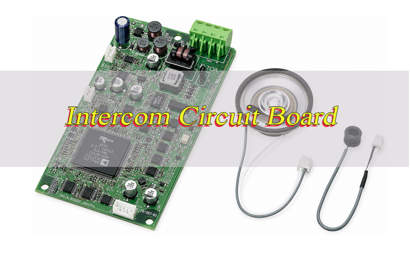
An intercom circuit board is the electronic platform that receives, processes, transmits and reproduces voice and control signals between communication stations. It is used in analog door-entry units, digital building systems, wireless handsets, IP intercoms and industrial communication terminals.
The board connects microphones, speakers, call buttons, displays, relays, power inputs and communication interfaces. A basic intercom PCB may use analog amplifiers and switching circuits, while an advanced design can include an MCU, DSP, audio codec, wireless module, Ethernet PHY and access-control output.
The circuit architecture depends on audio quality, communication distance, network type, enclosure size, power source and operating environment.
What Functions Does an Intercom PCB Control?
An intercom PCB controls audio capture, signal processing, communication, user commands and power distribution. The exact functions depend on whether the product is analog, digital, wired, wireless or IP-based.
Common functions include:
- Capturing voice through an electret or MEMS microphone
- Filtering and amplifying microphone signals
- Converting audio between analog and digital formats
- Driving speakers, handsets or headsets
- Supporting half-duplex or full-duplex communication
- Processing buttons, keypads and status indicators
- Controlling electric locks, relays and alarms
- Managing WiFi, Bluetooth, RF, Ethernet or two-wire connections
- Regulating input power into separate voltage rails
- Storing firmware, addresses and operating settings
- Protecting external interfaces against ESD and voltage surges
Stable performance requires these functions to operate without introducing noise, distortion or communication interference.
What Are the Main Components of an Intercom Circuit Board?
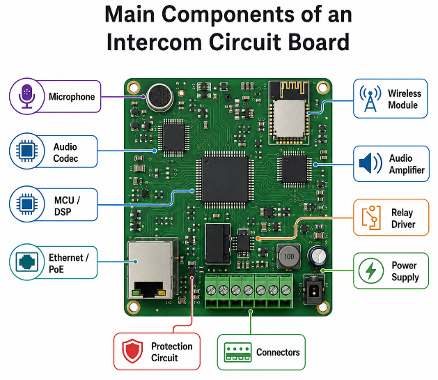
An intercom circuit board normally includes audio input, signal processing, communication, speaker output, power and protection circuits. The actual configuration depends on the system architecture and product functions.
| Component | Typical Selection | Main Function |
|---|---|---|
| Microphone | Electret, analog MEMS or digital MEMS | Captures voice |
| Microphone front end | Bias circuit, low-noise amplifier and filter | Conditions weak microphone signals |
| Audio codec | ADC, DAC and I²S interface | Converts analog and digital audio |
| Processor | MCU, DSP or application SoC | Controls audio, communication and system logic |
| Program memory | SPI NOR, EEPROM, NAND or eMMC | Stores firmware and configuration |
| Working memory | Internal SRAM or external DDR | Buffers audio and processing data |
| Audio amplifier | Class AB or Class D | Drives the speaker or handset |
| Speaker interface | Filter, protection and connector | Connects and protects the speaker output |
| Wireless circuit | Sub-GHz, Bluetooth or WiFi module | Provides wireless communication |
| RF network | Matching components, RF feed and antenna | Transfers RF energy to the antenna |
| Wired interface | Two-wire line interface or RS-485 transceiver | Supports wired communication |
| Ethernet interface | PHY, magnetics and RJ45 connector | Supports IP communication |
| PoE circuit | PoE PD controller and DC-DC converter | Receives power through Ethernet |
| Access-control output | Relay, MOSFET or transistor driver | Controls locks, alarms or gates |
| User interface | Buttons, keypad, LEDs or display driver | Processes commands and status |
| Clock and reset | Crystal, oscillator and reset IC | Controls timing and startup |
| Power supply | Buck, boost or LDO regulator | Generates stable voltage rails |
| Protection circuit | Fuse, TVS, ESD and reverse-polarity protection | Protects power and external interfaces |
| Debug interface | SWD, JTAG, UART or USB | Supports programming and diagnostics |
| Connector | Terminal block, FFC or board-to-board connector | Connects external devices |
A basic analog board may not require a processor, external memory or Ethernet circuit. An IP intercom with video, networking or an operating system may require a higher-performance SoC, DDR and eMMC.
The microphone front end, power supply, grounding, speaker amplifier and communication interface have the greatest influence on audio clarity and stability.
How to Read an Intercom Circuit Board Schematic and Block Diagram?
Read the functional block diagram first to understand the complete signal flow. Then use the schematic to verify how each circuit is powered, controlled and connected.
- Identify the system type: Confirm whether the product is analog, digital, two-wire, wireless or IP-based.
- Trace the power tree: Follow the input through the fuse, reverse-polarity protection, surge protection and voltage converters.
- Follow the microphone path: Check microphone bias, input protection, filters, amplifier gain and codec input.
- Review the processor section: Locate the MCU, DSP or SoC and check its clock, reset, memory, boot and programming circuits.
- Trace the speaker path: Follow the signal through the codec, amplifier, output filter and speaker connector.
- Inspect communication circuits: Review RF, Ethernet, RS-485 or two-wire interfaces separately.
- Check lock-control outputs: Confirm the relay or MOSFET driver, flyback protection and load connection.
- Review external connectors: Verify pin numbers, polarity, shielding, grounding and ESD protection.
- Compare with the PCB layout: Confirm that audio, RF, switching-power and speaker-current paths are separated.
- Check test access: Locate power, reset, programming, audio and communication test points.
This method helps identify incorrect voltages, excessive gain, missing protection and potential noise paths before production.
How Should a Wireless Intercom PCB Be Designed?
A wireless intercom PCB must balance RF performance, audio quality, power stability and mechanical constraints. These areas should be planned together because antenna placement, speaker current and switching noise can directly affect voice clarity and communication range.
Step 1: Define the product requirements.
Confirm the wireless protocol, operating frequency, communication range, microphone type, speaker power, input voltage, enclosure size and duplex mode. These requirements determine the processor, RF solution, audio circuit and PCB layer count.
Step 2: Choose the wireless solution.
A pre-certified wireless module can shorten development time and reduce RF certification risk. A discrete RF SoC provides more control over board size, antenna design and production cost but requires stronger RF design and testing capability.
Step 3: Plan the power system.
Separate the power needs of the processor, RF circuit, microphone front end and speaker amplifier. Use suitable converters, LDOs, decoupling capacitors and bulk capacitance to prevent RF transmission or high speaker volume from causing voltage drops and resets.
Step 4: Select the PCB layer structure.
A four-layer PCB is suitable for most wireless intercom products. One internal layer should provide a continuous ground plane, while another supports power distribution and low-speed signals. More layers may be required for external memory, Ethernet or dense routing.
Step 5: Divide the board into functional areas.
Separate the microphone circuit, processor, RF section, power converter and speaker amplifier. Keep low-level audio circuits away from switching nodes, inductors, crystals and high-current speaker traces.
Step 6: Position the antenna carefully.
Place the antenna near the PCB edge and follow the supplier’s keep-out requirements. Batteries, speakers, shields, cables, copper and metal fasteners should remain outside the antenna area because they can reduce range and change antenna tuning.
Step 7: Route the RF path correctly.
Keep the RF feed short and route it as a controlled 50 Ω transmission line. Maintain a continuous ground reference, avoid unnecessary vias and place the matching network close to the antenna or RF output.
Step 8: Protect the microphone signal.
Place microphone biasing, filtering and preamplification close to the microphone. Keep analog audio routes short and away from RF feeds, clocks, Class D outputs and switching regulators.
Step 9: Control speaker current paths.
Use short, wide traces for the amplifier supply, ground and speaker output. High-current return paths should not cross the microphone, codec or RF sections.
Step 10: Maintain a clean ground reference.
Use a continuous ground plane instead of unnecessary ground splits. Component placement and routing should control how audio, digital, RF and speaker currents return to the power source.
Step 11: Protect external interfaces.
Place ESD protection close to buttons, power inputs, charging ports and external connectors. Add reverse-polarity, surge or overcurrent protection according to the product environment.
Step 12: Add programming and test access.
Provide accessible points for power rails, reset, programming, microphone input, speaker output and communication signals. These points simplify prototype debugging and batch functional testing.
Step 13: Check heat dissipation.
Use copper areas and thermal vias around power amplifiers, regulators and other heat-generating parts. Keep these components away from microphones and temperature-sensitive RF parts.
Step 14: Review the enclosure design.
Confirm antenna clearance, microphone openings, speaker chambers, mounting holes and cable routes before releasing the PCB. The enclosure can affect wireless range, voice pickup and acoustic feedback.
Step 15: Test the complete product.
Verify pairing, communication range, reconnect behavior, audio clarity, standby current and maximum speaker volume inside the final enclosure. Testing should cover different distances, orientations, power conditions and nearby interference sources.
A reliable wireless intercom PCB depends on coordinated RF layout, clean audio routing, stable power delivery and enclosure-level testing.
How to Reduce Noise, Echo and Signal Interference in an Intercom PCB?
Noise and echo may come from power ripple, shared return paths, excessive gain, RF coupling, long cables or poor enclosure acoustics. The source should be identified before changing components or increasing amplifier power.
- Stabilize the power rails: Use suitable regulators, local decoupling and adequate bulk capacitance.
- Maintain continuous ground references: Avoid unnecessary ground-plane splits and control return paths through placement.
- Protect the microphone front end: Keep microphone routes short and away from regulators, clocks and speaker outputs.
- Separate high-current paths: Prevent amplifier and speaker currents from sharing narrow routes with the codec or microphone circuit.
- Set the gain correctly: Use only the required analog gain before the ADC to avoid clipping and amplified noise.
- Control RF coupling: Keep the RF section away from high-impedance audio nodes and follow antenna keep-out rules.
- Improve cable immunity: Use twisted pairs, differential signalling, shielding and suitable termination where possible.
- Reduce acoustic feedback: Increase microphone-to-speaker distance and use separate acoustic chambers.
- Apply digital processing: Use noise suppression, automatic gain control and acoustic echo cancellation.
- Validate under real conditions: Test different volume levels, cable lengths, wireless states and power sources.
PCB layout reduces electrical interference, but full-duplex echo normally requires both enclosure isolation and tuned echo-cancellation software.
What PCB Materials Are Suitable for Intercom Circuit Board?
Standard FR-4 is suitable for most intercom circuit boards because it provides adequate electrical performance, mechanical strength and manufacturing availability. Material selection should follow the operating temperature, wireless frequency, circuit density and environmental conditions.
- Standard FR-4: Suitable for basic analog intercoms, indoor door stations and low-density wired communication boards.
- High-Tg FR-4: Recommended for outdoor systems, repeated lead-free assembly and products exposed to wider thermal cycles.
- Controlled-Dk FR-4: Suitable for wireless and IP intercoms that require controlled RF or high-speed impedance.
- Low-loss RF material: Used when RF routes are long, insertion loss is critical or operating frequency exceeds the practical performance of standard FR-4.
- Flexible PCB: Suitable for connecting microphones, keypads, displays and controls in compact or movable assemblies.
- Rigid-flex PCB: Reduces connectors and cables in products with limited internal space.
- Metal-core PCB: Rarely used for the main board but may support separate high-power lighting or thermal modules.
Material evaluation should consider Tg, Td, Dk, Df, moisture absorption, z-axis expansion, CAF resistance, copper weight and finished thickness.
For most digital and wireless intercom products, high-Tg or controlled-Dk FR-4 provides sufficient performance without the cost of a full RF laminate.
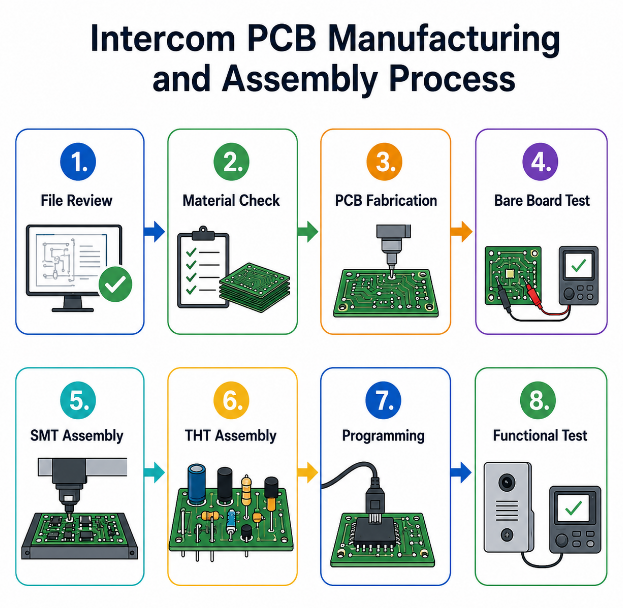
How Are Intercom Circuit Boards Manufactured and Assembled?
Intercom circuit board production combines bare-board fabrication, component assembly, programming and functional verification. Each stage should control materials, solder quality, firmware versions and audio performance.
Step 1: Review the production files.
Check Gerber or ODB++ data, drill files, stackup, controlled-impedance requirements, BOM, centroid data, assembly drawings, firmware and test specifications. Footprints, polarity, antenna restrictions and missing test points should be corrected before production.
Step 2: Confirm materials and components.
Verify the laminate, copper weight, finished thickness, surface finish and impedance structure. Component manufacturers, package sizes, lifecycle status, moisture sensitivity and approved substitutions should also be confirmed.
Step 3: Form the inner-layer circuits.
Image, develop and etch the inner copper layers. Inspect line width, spacing, copper balance and layer registration before lamination.
Step 4: Laminate the multilayer PCB.
Align the copper cores and prepreg, then press them together under controlled temperature and pressure. Lamination quality affects board thickness, dielectric spacing and impedance consistency.
Step 5: Drill and plate the holes.
Drill vias, component holes and mounting holes, then clean the hole walls and deposit copper. Final plating connects the copper layers and provides the required finished hole size.
Step 6: Form the outer-layer circuits.
Image and etch the outer copper patterns, then inspect trace dimensions, pad geometry and copper thickness. Controlled RF and high-current routes require close dimensional control.
Step 7: Apply solder mask and surface finish.
Add solder mask and legend before applying ENIG, lead-free HASL or another specified finish. Microphone pads, fine-pitch devices and connectors require accurate solder-mask openings.
Step 8: Inspect the bare PCB.
Perform electrical testing for opens and shorts, followed by dimensional and visual inspection. Controlled-impedance coupons should be measured when RF or Ethernet routes require impedance verification.
Step 9: Prepare the assembly process.
Review stencil openings, solder-paste type, feeder setup, component polarity and reflow requirements. Moisture-sensitive PCBs and components should be stored or baked according to their handling level.
Step 10: Assemble the SMT components.
Print solder paste onto the pads and use SPI to check deposit volume and alignment. Place resistors, processors, codecs, MEMS microphones, RF modules and other SMT parts before controlled reflow soldering.
Step 11: Install through-hole components.
Assemble terminal blocks, relays, switches, transformers and large connectors. Selective soldering, wave soldering or manual soldering can be used according to component layout and volume.
Step 12: Inspect the completed PCBA.
Use AOI to check placement, polarity and visible solder joints. X-ray inspection should be used for QFN, LGA, BGA and other bottom-terminated packages with hidden connections.
Step 13: Clean and program the board.
Remove process residues when cleaning is required, then load firmware, serial numbers, MAC addresses and configuration data. Programming results should be verified through read-back or functional checks.
Step 14: Complete functional testing.
Verify voltage rails, operating current, microphone input, speaker output, audio loopback, buttons, indicators, relays and wired or wireless communication. Testing should use the specified microphone, speaker load and firmware version.
Step 15: Approve the first article and release production.
Confirm the first completed units before batch assembly. Approved PCB files, BOM revisions, component substitutions, firmware versions and test results should be recorded for repeat-order traceability.
A controlled manufacturing and assembly process reduces solder defects, audio inconsistency, programming errors and performance differences between production batches.
What Testing Is Required for an Intercom Circuit Board Assembly?
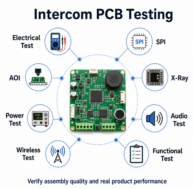
Testing should verify soldering quality, electrical operation, audio performance and communication stability. Acceptance limits should be defined from the product specification.
- Bare-board electrical testing: Detect opens, shorts and incorrect connections.
- SPI: Check solder paste volume, alignment and bridging risk.
- AOI: Inspect component presence, polarity, placement and visible solder joints.
- X-ray inspection: Examine joints under QFN, LGA, BGA and other bottom-terminated packages.
- Power-up testing: Measure input current, startup behavior, voltage rails, ripple and abnormal heating.
- Programming verification: Confirm firmware, configuration, serial number and read-back results.
- Microphone testing: Check bias voltage, sensitivity, gain, background noise and channel operation.
- Speaker-output testing: Verify output power, response, clipping, distortion and idle noise.
- Audio-loopback testing: Confirm the complete microphone-to-speaker signal path.
- Full-duplex testing: Check echo suppression, gain stability and feedback margin.
- Wired communication testing: Verify polarity, data integrity and operation over the specified cable length.
- Wireless communication testing: Check pairing, stability, reconnect behavior and practical range.
- User-interface testing: Verify buttons, keypads, indicators, call tones and volume controls.
- Access-control testing: Test relay or MOSFET outputs under the intended load.
- Protection testing: Evaluate reverse polarity, ESD and surge resistance where required.
- Environmental testing: Perform temperature, humidity, vibration or burn-in tests based on the application.
- Final system testing: Test the PCBA with the specified microphone, speaker, firmware, cables and enclosure.
Audio limits such as sensitivity, output power, SNR, frequency response and THD+N should be agreed before production.
What Custom Intercom PCB Design and Assembly Services Can We Provide?
EBest Circuit provides one-stop intercom PCB and PCBA support from design review to repeat production.
- Intercom PCB design: Schematic review, layout, grounding, audio routing, RF routing and antenna planning.
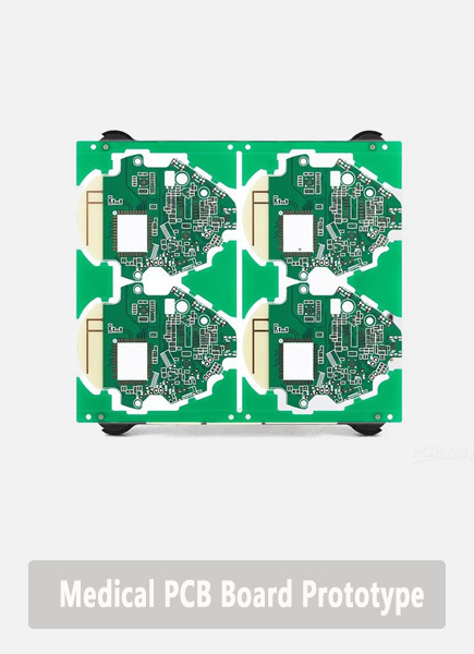
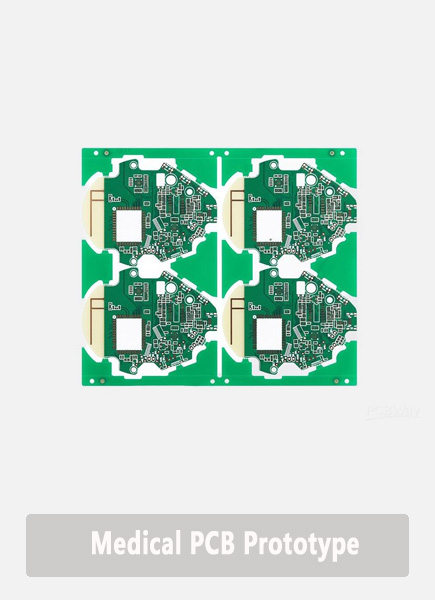
- PCB prototype: Quick-turn boards for electrical, acoustic, wireless and enclosure validation.
- PCB manufacturing: FR-4, high-Tg, RF, HDI, flexible and rigid-flex PCB production.
- Component sourcing: BOM review, lifecycle checks, procurement and approved substitution support.
- PCB assembly: SMT, THT and mixed assembly for prototypes, pilot runs and batch orders.
- Fine-pitch assembly: Support for 01005 components, QFN, LGA and BGA packages down to 0.25 mm pitch.
- Firmware programming: MCU firmware, serial numbers, MAC addresses and configuration data.
- Inspection and testing: SPI, AOI, X-ray, first-article inspection and customized functional testing.
- Box assembly: Enclosure installation, cable connection, labeling and final product assembly.
Send your Gerber files, BOM, assembly drawings and test requirements to sales@bestpcbs.com for evaluation.
Custom Wireless Intercom Circuit Board Manufacturing and Assembly Case Study
Project background:
A compact wireless intercom product required two-way voice communication, button control and speaker output within a limited enclosure. The project also required stable wireless performance, clear audio, firmware programming and repeatable PCBA production.
Project requirements:
- 4-layer FR-4 PCB
- 1.0 mm finished board thickness
- 1 oz copper
- 2.4 GHz wireless communication
- Digital MEMS microphone
- 4 Ω, 3 W speaker output
- 12 V DC input
- Controlled 50 Ω RF impedance
- Firmware and serial-number programming
- Audio and wireless functional testing
- Prototype and repeat production support
Our solution:
- Design review: Reviewed the schematic, PCB layout, stackup, BOM and test requirements before production.
- Functional zoning: Separated the microphone, processor, RF, power and amplifier sections to reduce interference.
- RF optimization: Routed the RF feed with controlled 50 Ω impedance and placed the antenna keep-out area near the PCB edge.
- Audio protection: Kept the microphone input away from switching regulators, clocks and speaker-current routes.
- Power stability: Added suitable decoupling capacitors, filtering components and short power-return paths.
- Test access: Added test points for voltage rails, audio signals, programming and communication checks.
- Assembly control: Used SPI, AOI and X-ray inspection to verify solder paste, component placement and hidden joints.
- Programming: Loaded firmware, serial numbers and configuration data after assembly.
- Functional testing: Verified power, microphone input, audio loopback, speaker output, buttons and wireless connection.
Project result:
The pilot boards passed the specified power, audio, control and wireless communication tests. After first-article approval, the PCB files, BOM, firmware version and test requirements were released for controlled repeat production.
The completed manufacturing package supported consistent assembly, programming and testing across subsequent orders.
Why Choose EBest Circuit as Your Intercom PCB Manufacturer?
EBest Circuit integrates design support, PCB production, sourcing, assembly and testing to reduce project handoffs and improve production control. Here are reasons why choose EBest Circuit as your intercom PCB manufacturer:
- One-stop project management: Design review, PCB fabrication, sourcing, assembly, programming and testing are coordinated through one supplier.
- Fewer prototype failures: Manufacturing and assembly risks are identified before fabrication, reducing avoidable redesigns.
- Faster product validation: Prototype assembly supports early testing of audio, RF, power and enclosure performance.
- Flexible order volumes: Support is available for prototypes, low-volume builds, pilot runs and mass production.
- Fine-pitch capability: Assembly supports 01005 components and BGA pitches down to 0.25 mm.
- Mixed assembly support: SMT, THT and mixed processes support processors, microphones, relays and large connectors.
- Risk-based inspection: SPI, AOI, X-ray and functional tests are selected according to the board design.
- Stable sourcing support: BOM review and controlled substitutions reduce shortage-related delays.
- Quality-system support: Available certifications include ISO 9001, IATF 16949, ISO 13485, AS9100D, UL, RoHS and REACH.
- Repeat-order consistency: Approved files, BOM revisions, firmware and test requirements can be retained for future production.
- China manufacturing with global supply: Custom intercom PCB products are manufactured in China and delivered internationally.
FAQs About Intercom Circuit Boards
Q1: Can a discontinued intercom board be replaced with a newly designed board?
A1: Yes, but the new board must match the original voltage, connector pinout, microphone type, speaker impedance and lock-control method. Mounting holes and enclosure dimensions should also be confirmed before redesign.
Q2: How many assembled boards should be ordered for the first prototype run?
A2: A first build of 5–20 assembled boards is practical for firmware debugging, acoustic testing, wireless validation and enclosure fitting. This quantity also helps separate design problems from individual assembly defects.
Q3: Can a 4 Ω speaker replace an 8 Ω intercom speaker?
A3: Only if the amplifier supports a 4 Ω load. Lower impedance increases current and may cause distortion, overheating or power-supply droop. Check the amplifier rating and speaker power before replacement.
Q4: Should an intercom use an electret or MEMS microphone?
A4: Electret microphones are low-cost but require careful biasing and filtering. MEMS microphones are smaller and provide more consistent sensitivity. The choice depends on board space, pickup distance, interface and operating environment.
Q5: Can existing building wiring be reused for a new intercom system?
A5: Yes, when the cable condition, resistance, insulation and topology meet the new system requirements. Existing analog wiring may not support Ethernet or high-speed digital communication, so continuity and voltage-drop tests are required.
Q6: Does an outdoor intercom board require conformal coating?
A6: Conformal coating is recommended for humidity, condensation, dust or salt exposure. Typical coating thickness is 25–75 μm. Microphones, connectors, antennas and test points may require masking.
Q7: Can firmware, serial numbers and MAC addresses be loaded during assembly?
A7: Yes. Firmware and identification data can be programmed through SWD, JTAG, UART, USB or test pads. Read-back or functional testing should confirm that the correct data was loaded.
Q8: How should obsolete components be managed in a long-life intercom product?
A8: Check the lifecycle status of processors, codecs, RF modules, memory and connectors before production. Approved alternatives, planned last-time purchases and controlled redesigns help reduce supply interruptions.
Q9: Can an intercom board be designed for future feature upgrades?
A9: Yes. Reserve programming access, test points, memory capacity and selected optional interfaces. However, unnecessary circuits should be avoided because they increase board size, cost and validation work.
Q10: What should be checked before approving the first assembled sample?
A10: Confirm the PCB revision, BOM, firmware, polarity, power consumption and connector functions. Test the microphone, speaker, controls, relays and communication interfaces before batch production.
Q11: Can EBest Circuit assemble boards with supplied components?
A11: Yes. Components can be customer-supplied, partially supplied or fully sourced. Clear part numbers, quantities, packaging and moisture-sensitivity information should be provided before assembly.
Q12: Is final box assembly available after PCBA production?
A12: Yes. Box assembly can include enclosure installation, cable connection, labeling, firmware loading and final functional inspection. Mechanical drawings and acceptance criteria should be supplied in advance.
Q13: How can an intercom PCB be made easier to repair?
A13: Use clear labels, accessible test points and replaceable modules. Programming connectors and frequently serviced parts should remain accessible after final assembly.
Q14: How can repeated orders maintain consistent quality?
A14: Keep PCB files, BOMs, firmware versions and test limits under revision control. Record material lots, component batches and inspection results for each production run.
Q15: What information should be included in an intercom PCBA purchase order?
A15: Include PCB revision, BOM, quantity, delivery date, firmware version, test scope and packaging requirements. Clearly identify supplied parts, approved alternatives and programming rules.
A reliable intercom circuit board project requires coordinated audio design, RF control, material selection, component sourcing, assembly and functional testing. Before production, confirm the operating voltage, communication method, microphone type, speaker load, enclosure restrictions, firmware version and acceptance limits.
For custom intercom PCB design, prototype manufacturing, component sourcing, PCB assembly or repeat production, send your Gerber files, BOM, assembly drawings and test requirements to EBest Circuit via sales@bestpcbs.com.