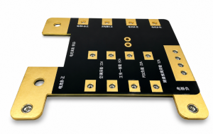
An IP camera PCB combines image capture, video processing, power conversion, storage, audio and network communication on one compact platform. Its design directly affects image quality, connection stability, operating temperature and product life.
This IP camera PCB design guide explains how the main board works, which components and materials it uses, and how to control PoE power, WiFi performance, night vision circuits, signal integrity and thermal risks. It also covers manufacturing, assembly and production support from prototype through mass production.
Are you worried about these problems of IP camera PCB design, manufacturing and assembly?
- Are IP camera PCB design issues causing image noise, unstable Ethernet, poor WiFi performance or overheating?
- Are component shortages, engineering changes or uncontrolled production schedules delaying your IP camera PCB manufacturing?
- Are BGA, QFN, programming or testing defects reducing IP camera PCB assembly consistency?
EBest Circuit provides practical design, manufacturing and assembly solutions for IP camera PCB projects. Below are our solutions to these problems:
- Design optimization: Review schematics, stackups, impedance, MIPI routing, PoE isolation, RF layout and thermal paths before production.
- Production control: Verify materials, components and manufacturing files to reduce shortages, hidden costs and delivery delays.
- Assembly assurance: Apply SPI, AOI, X-ray inspection, programming and functional testing to control soldering and performance risks.
From prototype to mass production, EBest Circuit helps improve product reliability, delivery stability and cost control. Send your Gerber files, BOM and project requirements to sales@bestpcbs.com for a quotation.
What Is an IP Camera PCB?
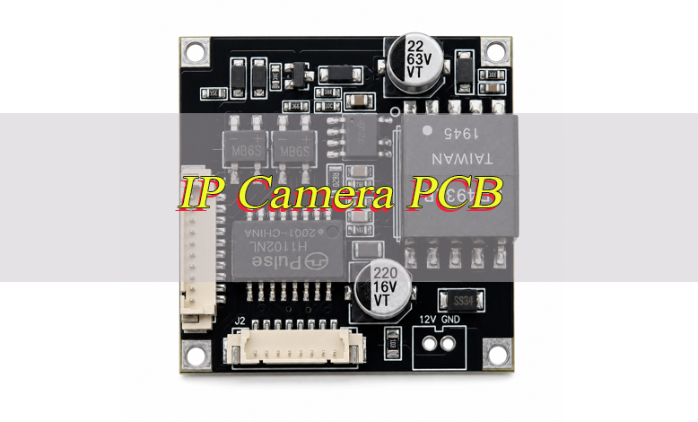
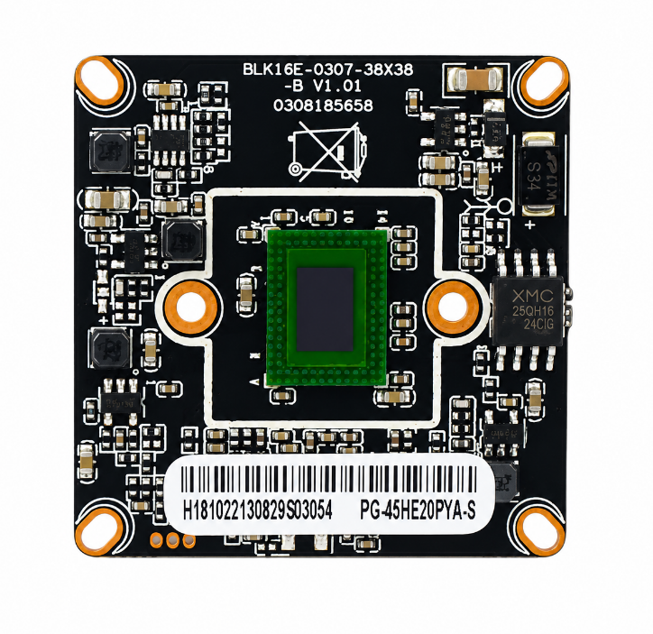
An IP camera PCB is the main electronic board that captures, processes, compresses and transmits video through an IP network. It connects the image sensor with the processor, memory, power system, Ethernet or WiFi interface, local storage, audio circuits and night vision system.
Unlike a basic analog camera board, an IP camera PCB normally runs embedded firmware and supports remote viewing, video compression, motion detection and network management. Depending on the product, it may also control AI image analysis, alarm inputs, motorized lenses, heaters or pan-tilt mechanisms.
Common applications include:
- Dome security cameras
- Bullet cameras
- Doorbell cameras
- Pan-tilt-zoom cameras
- Battery-powered WiFi cameras
- Outdoor PoE surveillance cameras
- Industrial monitoring cameras
- AI recognition cameras
- Smart home camera modules
The main design challenge is functional density. High-speed image data, switching power circuits, RF communication and heat-generating processors must operate inside a compact enclosure without interfering with one another.
What Are the Main Components of an IP Camera PCB Board?
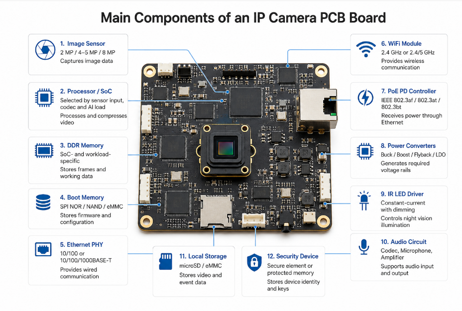
An IP camera PCB is not defined by one processor or one fixed memory capacity. Its component architecture must match the required resolution, frame rate, video compression, AI functions, network type and night vision range. The following table lists the core components normally found on an IP camera main board.
| Component | Typical Selection | Function |
|---|---|---|
| Image sensor | 2 MP, 4/5 MP or 8 MP | Captures image data |
| Processor or SoC | Selected by sensor input, codec and AI load | Processes and compresses video |
| DDR memory | SoC- and workload-specific | Stores frames and working data |
| Boot memory | SPI NOR, NAND or eMMC | Stores firmware and configuration |
| Ethernet PHY | 10/100 or 10/100/1000BASE-T | Provides wired communication |
| WiFi module | 2.4 GHz or 2.4/5 GHz | Provides wireless communication |
| PoE PD controller | IEEE 802.3af, 802.3at or 802.3bt | Receives power through Ethernet |
| Power converters | Buck, boost, flyback or LDO | Generates required voltage rails |
| IR LED driver | Constant-current with dimming | Controls night vision illumination |
| Audio circuit | Codec, microphone and amplifier | Supports audio input and output |
| Local storage | microSD or eMMC | Stores video and event data |
| Security device | Secure element or protected memory | Stores device identity and keys |
A typical IP camera PCB architecture follows this signal path: image sensor → MIPI CSI-2 → processor or ISP → DDR memory → video encoder → Ethernet or WiFi interface.
Audio, storage, PoE and night vision circuits support this main data path without interfering with image processing or network communication. Component selection should therefore be based on the complete system workload rather than isolated specification values.
How Does an IP Camera PCB Process Video, Audio, Power and Network Signals?
An IP camera PCB handles several signal types at the same time. The main video path is lens → image sensor → MIPI interface → processor → memory → video encoder → Ethernet or WiFi network.
The image sensor converts incoming light into raw digital image data. The processor or image signal processor adjusts exposure, white balance, color, noise reduction, contrast and wide dynamic range before compressing the video into formats such as H.264 or H.265.
Audio enters through a microphone and low-noise amplifier. An audio codec converts the analog signal into digital data before the processor synchronizes it with the video stream. Two-way audio products also include a digital-to-analog converter and speaker amplifier.
The power section accepts a PoE input or external DC supply and creates the voltage rails required by the processor, sensor, memory, Ethernet PHY and peripheral circuits. These rails must start in the correct order and remain within the ripple limits specified by the component manufacturers.
Network data passes through the Ethernet PHY or WiFi module. The processor packages compressed video, audio and control information into IP packets for live viewing, recording, event detection and remote device management.
How to Read an IP Camera PCB Schematic and Functional Block Diagram?
An IP camera schematic can look complicated because power, video, memory, network and peripheral circuits are shown across several pages. The clearest reading method is to identify the main functional blocks first, then follow power, data and control signals between them.
- Start with the functional block diagram. Identify the image sensor, processor, memory, Ethernet, WiFi, power, audio, storage and night vision sections before reviewing individual components.
- Map the complete power tree. Trace the input from PoE or a DC connector through protection, conversion and regulation stages. Record each voltage rail, current demand, enable signal and startup sequence.
- Locate the processor support circuits. Check the oscillator, reset circuit, boot configuration, watchdog, flash memory, debugging interface and programming connector.
- Trace the image signal path. Follow the sensor clock, I2C control bus and MIPI CSI-2 lanes from the image sensor to the processor. Confirm connector pin order, lane polarity and power sequencing.
- Review the memory interfaces. Check DDR address, data, clock and control groups together. Verify reference voltage, termination, decoupling and routing between the processor and memory.
- Inspect Ethernet and PoE separately. Follow Ethernet data through the PHY, magnetics, protection devices and RJ45 connector. Then trace PoE power through the bridge rectifier, PD controller and DC-DC converter.
- Check the wireless section. Identify the WiFi module, RF matching network, antenna connector, antenna keepout and local power filtering.
- Review peripheral circuits. Confirm the microSD interface, microphone, speaker amplifier, light sensor, IR LED driver, IR-cut filter motor and alarm or motor-control connections.
- Find test and programming points. Power rails, reset, UART, JTAG, Ethernet status and critical control signals should remain accessible during prototype debugging and production testing.
A complete review should confirm that each functional block receives the correct power, reference plane and control signals. It should also identify where noisy switching currents, high-speed routes or missing test points could create problems during bring-up or mass production.
What PCB Materials and Stackup Are Suitable for IP Camera Main Boards?
The stackup must support high-speed image data, stable power distribution, compact BGA routing and practical heat spreading. Most IP camera main boards use high-Tg FR-4 with a 4-layer, 6-layer or 8-layer structure, but the final choice depends on processor density, interface speed and board size.
A 4-layer board may support a simple camera using an integrated processor module and limited interfaces. A 6-layer structure provides stronger reference planes, cleaner power distribution and more routing space. An 8-layer or HDI PCB is more suitable for fine-pitch BGA processors, DDR memory, AI functions or several high-speed interfaces.
| Parameter | Typical Range | Selection Basis |
|---|---|---|
| Layer count | 4–8 layers | Density and signal speed |
| Board thickness | 0.8–1.6 mm | Enclosure and connector requirements |
| Finished copper | 1–2 oz | Current and thermal load |
| Material Tg | 150–170°C | Reflow and operating temperature |
| Surface finish | ENIG or lead-free HASL | Pitch and assembly requirements |
| Impedance tolerance | ±10% | High-speed interface control |
| Minimum line/space | 3/3–5/5 mil | BGA and HDI requirements |
| Minimum mechanical via | 0.15–0.30 mm | Stackup and routing density |
A practical 6-layer structure may use:
| Layer | Type | Routing Use |
|---|---|---|
| L1 | Signal | Components and short critical routes |
| L2 | GND | Continuous reference plane |
| L3 | Signal | Internal high-speed routing |
| L4 | Power | Main power distribution |
| L5 | GND | Return path and shielding |
| L6 | Signal | Secondary routing and components |
MIPI, DDR, Ethernet and clock routes should remain next to continuous GND planes. The selected stackup should also provide realistic BGA escape routing, stable impedance and enough copper for thermal spreading.
How Should Power Delivery and Protection Be Designed for a PoE IP Camera PCB?
PoE design affects more than whether the camera powers on. An unstable PoE section can cause startup failure, Ethernet disconnection, image noise, excessive heat or repeated resets during night vision operation. The design must control input protection, classification, conversion, isolation, power sequencing and thermal performance as one complete system.
- Define the PoE type and power class first. Calculate the maximum load from the processor, image sensor, WiFi module, IR LEDs, heater, motors and external peripherals.
- Arrange components in power-flow order. A practical sequence is RJ45 connector → Ethernet magnetics → bridge rectifiers → input protection → PoE PD controller → DC-DC converter.
- Verify detection and classification. The signature resistance, classification circuit, inrush control and maintain-power signature must match the selected controller and required PoE class.
- Design for the full input range. The converter must remain stable across the minimum and maximum voltage specified by the selected PoE standard.
- Add cable-side protection. Use suitable TVS devices, common-mode protection and input filtering against ESD, surge and cable-induced transients.
- Keep switching loops compact. Place the transformer, MOSFET, rectifier and high-frequency capacitors close together. Keep switching nodes away from image, audio and Ethernet circuits.
- Maintain isolation and spacing. Where isolation is required, provide sufficient creepage and clearance between the PoE input and low-voltage output sections.
- Control power sequencing. Confirm that the processor, DDR, image sensor and peripheral rails start in the order required by the chipset.
- Improve heat dissipation. Use copper areas and thermal vias around the PD controller, MOSFET, transformer and rectifier. Keep these heat sources away from the image sensor.
- Validate abnormal conditions. Test minimum and maximum input voltage, long cable operation, startup load, overload, short circuit, power cycling, surge and high-temperature operation.
A reliable PoE section should start correctly under different cable lengths and load conditions, maintain clean low-voltage rails and avoid transferring switching noise into the sensor or network circuits.
How Should Wireless Connectivity Be Designed for a WiFi IP Camera PCB?
WiFi range is often limited by board placement and enclosure design rather than by the wireless module itself. Antenna clearance, RF trace quality, power stability and nearby metal parts all influence throughput and connection reliability.
- Select the wireless architecture first. Confirm the WiFi standard, 2.4 GHz or dual-band operation, antenna type, target throughput and regional certification requirements.
- Place the module near the board edge. An integrated antenna should sit at or beyond the host-board edge where the module guidelines allow it.
- Follow the specified antenna keepout. Remove copper, traces and components from the antenna area according to the module manufacturer’s drawing.
- Control the external RF feed. When using an external antenna, route the feed as a short 50 Ω transmission line with minimal vias and smooth bends.
- Separate RF from noise sources. Keep the antenna away from switching regulators, DDR clocks, MIPI lanes, PoE transformers, IR LED drivers and high-current wiring.
- Provide stable module power. Place local decoupling capacitors close to the module and ensure the regulator can support transmit-current peaks without excessive voltage drop.
- Protect exposed RF connections. Use a low-capacitance ESD protection device when an external antenna connector is accessible.
- Review the complete enclosure. Batteries, cables, screws, shields, lens holders and brackets can block or detune the antenna.
- Test the final product. Measure connection stability, throughput and range after the complete camera has been assembled in its intended enclosure.
Open-board RF testing is not enough. Final verification should use the actual enclosure, cable routing and mounting structure because these parts can reduce range even when the WiFi IP camera PCB layout appears correct.
How Should an IP Camera PCB Support Infrared LEDs and Night Vision Circuits?
Night vision quality depends on more than selecting high-power infrared LEDs. The driver, light sensor, IR-cut filter, image exposure and thermal path must work together. Poor coordination can cause flicker, uneven illumination, repeated day-and-night switching or image degradation caused by heat.
- Choose the IR wavelength by application. An 850 nm LED normally provides stronger sensor response and longer range, while a 940 nm LED reduces visible red glow.
- Use a constant-current driver. Stable current prevents brightness changes caused by input-voltage variation and LED forward-voltage tolerances.
- Add controllable dimming. PWM or analog dimming allows illumination to match exposure, scene distance and ambient-light conditions.
- Balance multiple LED strings. Multi-string arrays require current balancing so that one string does not operate brighter or hotter than the others.
- Include ambient-light measurement. A light sensor should control day-and-night switching based on the actual illumination level.
- Add hysteresis and delay. These functions prevent repeated switching when the measured light level remains close to the threshold.
- Control the IR-cut filter correctly. The motor or solenoid driver should provide the required pulse direction and duration without continuous coil current.
- Separate the LED power loop. Keep high-current LED traces and PWM switching nodes away from sensor power, microphones, clocks and MIPI routes.
- Design an effective thermal path. Use wide copper, thermal vias or a separate LED board when the illumination circuit produces significant heat.
- Synchronize pulsed illumination when required. IR LED pulses may need to align with sensor exposure to prevent bands, flicker or uneven brightness.
- Verify optical and thermal performance. Test illumination distance, image uniformity, enclosure temperature and sensor temperature at maximum LED current.
A separate illumination PCB is often preferable for cameras with long night vision range. It keeps LED heat away from the image sensor and gives the main board more space for high-speed routing and thermal control.
How to Design a Compact IP Camera PCB Without Signal or Thermal Problems?
A smaller board can reduce enclosure size, but aggressive component compression often creates new signal, RF and thermal problems. The correct approach is to fix the optical and mechanical requirements first, then organize the board around critical signal paths, heat sources and manufacturing limits.
Step 1: Fix the mechanical and optical constraints.
Confirm the board outline, sensor position, optical axis, lens holder, mounting holes, connector direction and maximum component height before placement.
Step 2: Select the board architecture.
Decide whether the product should use one main PCB or separate sensor, processor and illumination boards. Multiple boards can improve optical alignment, thermal separation and assembly access.
Step 3: Divide the PCB into functional zones.
Separate the image sensor, processor, DDR, Ethernet, PoE, WiFi, audio and IR LED sections. Keep switching noise and heat away from sensitive image circuits.
Step 4: Define the stackup and impedance.
Provide continuous GND reference planes for MIPI, DDR, Ethernet and RF routes. Confirm controlled-impedance dimensions with the PCB manufacturer before routing.
Step 5: Place critical components first.
Keep the sensor and processor close enough to shorten MIPI routes. Place DDR close to the processor and position regulators close to their loads without heating the sensor.
Step 6: Route high-speed signals first.
Maintain differential-pair geometry, avoid plane splits, limit unnecessary vias and keep clocks away from the antenna region.
Step 7: Complete power and grounding.
Use compact regulator loops, local decoupling, solid return paths and enough copper for high-current rails.
Step 8: Build the thermal path.
Add thermal vias beneath exposed pads, connect heat sources to internal copper and provide enclosure contact areas where mechanical heat transfer is available.
Step 9: Review manufacturability and testing.
Check BGA escape routing, solder-mask clearances, component spacing, rework access, programming points and functional-test connections.
Step 10: Validate the assembled enclosure.
Test image quality, WiFi range, PoE operation and component temperatures during maximum video load and full night vision operation.
The final design should remain compact without blocking the antenna, raising the image sensor temperature or interrupting high-speed return paths. Board size is only successful when electrical, thermal and production performance remain stable.
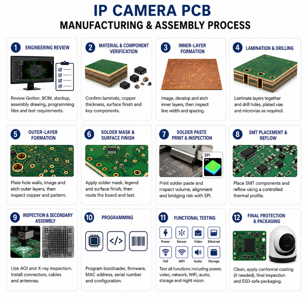
What Is the IP Camera PCB Manufacturing and Assembly Process?
IP camera PCB production includes more than bare-board fabrication and component placement. The process must also control material traceability, solder quality, firmware versions, programmed identities and functional performance.
Step 1: Complete engineering review.
Check Gerber or ODB++ data, drill files, stackup, controlled impedance, BOM, centroid file, assembly drawing, programming files and test requirements.
Step 2: Verify materials and components.
Confirm laminate, copper thickness, surface finish, component manufacturers, package sizes, moisture sensitivity and approved substitutions.
Step 3: Form the inner-layer circuits.
Image, develop and etch the inner copper layers, then inspect line width, spacing and registration before lamination.
Step 4: Laminate and drill the PCB.
Press the copper and dielectric layers together before drilling mechanical holes, plated vias and laser microvias where required.
Step 5: Plate and form the outer layers.
Plate the hole walls, image and etch the outer circuits, then inspect copper thickness and pattern accuracy.
Step 6: Apply solder mask and surface finish.
Add solder mask, legend and the selected finish before routing the board outline and completing electrical and impedance testing.
Step 7: Print and inspect solder paste.
Use an approved stencil design and inspect paste volume, alignment and bridging risk with SPI before component placement.
Step 8: Place and reflow SMT components.
Mount the processor, memory, power and communication components before running the assembly through a controlled reflow profile.
Step 9: Inspect and complete secondary assembly.
Use AOI for visible joints and X-ray for BGA, QFN and hidden thermal pads. Install through-hole connectors, cables and antennas afterward.
Step 10: Program each assembly.
Load the bootloader, firmware, MAC address, serial number and configuration data using controlled revision records.
Step 11: Perform functional testing.
Check input current, voltage rails, startup sequence, sensor communication, video streaming, Ethernet, PoE, WiFi, audio, storage and night vision.
Step 12: Complete final protection and packaging.
Clean the PCBA where required, apply conformal coating only to approved areas, complete final inspection and pack the boards in ESD-safe materials.
A controlled process should link the PCB revision, component lot, firmware version, MAC address and test result. This traceability makes prototype problems easier to investigate and improves batch consistency during repeat production.
What IP Camera PCB Design, Manufacturing and Assembly Services Can We Provide?
EBest Circuit supports IP camera projects from initial board development to assembled products. Combining PCB fabrication, component sourcing and assembly under one production system reduces supplier handoffs and simplifies production control.
- PCB design: Schematic review, PCB layout, stackup planning, impedance control and manufacturability analysis.
- PCB prototyping: Small-volume builds for hardware bring-up, firmware development and design verification.
- PCB manufacturing: FR-4, multilayer, HDI, high-Tg, high-speed and impedance-controlled PCB production.
- Component sourcing: Supply support for processors, memory, PoE devices, WiFi modules, BGA, QFN and passive components.
- SMT assembly: Placement of components down to 01005 packages and BGA pitches down to 0.25 mm.
- Through-hole assembly: Installation of connectors, transformers, switches and other leaded components.
- Mixed assembly: Combined SMT and through-hole processing for complete IP camera main boards.
- Prototype assembly: Quick-turn assembly for engineering samples and design revisions.
- Mass production: Scalable PCB and PCBA production after prototype approval.
- Box assembly: PCB installation, cable connection, enclosure integration and final product assembly.
- Mechanical support: Injection molding, CNC machining, sheet-metal fabrication, laser engraving and surface finishing.
- Final inspection: Complete inspection before delivery according to approved drawings and acceptance requirements.
Why Choose EBest Circuit as Your IP Camera PCB Manufacturer?
IP camera PCB production requires high-density assembly, stable component sourcing and consistent control from prototype to volume manufacturing. EBest Circuit combines these capabilities in one production workflow.
- Fewer supplier handoffs: PCB fabrication, component sourcing, assembly and box build can be managed through one production system.
- Faster project transition: Prototype, quick-turn assembly and mass production support a smoother move from design verification to repeat orders.
- Fine-pitch assembly capability: Support for 01005 components, 0.25 mm BGA pitch, SMT, THT and mixed assembly fits compact camera boards.
- Scalable production capacity: Monthly PCB capacity reaches approximately 260,000 square feet, with placement capacity of 13.2 million components per day.
- Flexible PCB technologies: Available options include HDI PCB, high-Tg PCB, high-speed PCB, impedance-controlled PCB, flexible and rigid-flex PCB.
- Stable component supply: An established supply chain supports SMD components, BGA, QFN, QFP and other electronic parts.
- Short lead-time options: PCBA lead times can start from 1–5 days, while qualified urgent PCB orders may support shipment in as little as 24 hours.
- Lower coordination costs: Box assembly, injection molding, CNC machining and sheet-metal services reduce the need to manage separate mechanical suppliers.
- Recognized quality systems: Certifications include ISO 9001:2015, IATF 16949, ISO 13485:2016, AS9100D, UL, RoHS and REACH.
- Global supply from China: Production and shipment are managed from China without false overseas factory or warehouse claims.
Compact PoE IP Camera Main Board Manufacturing and Assembly Case Study
This representative project shows how PCB design review, component sourcing, fine-pitch assembly, programming and production control can be integrated for a compact PoE security camera main board. Confidential product names, firmware and proprietary circuit details are excluded.
Project Background
A security camera developer required a compact main board for an outdoor PoE camera. The design combined a fine-pitch BGA video processor, DDR memory, Ethernet communication, PoE power conversion, local storage and night vision control inside a restricted enclosure.
The initial project involved separate PCB, component and assembly suppliers. This increased communication time and made it difficult to control design revisions, component substitutions and production records.
Project Requirements
- Multilayer impedance-controlled PCB
- Fine-pitch BGA and QFN assembly
- Compact processor and memory placement
- Stable sourcing for processor, memory and PoE components
- SMT and through-hole mixed assembly
- Prototype production followed by repeat manufacturing
- Consistent inspection before shipment
- Firmware, MAC address and serial number programming
- Enclosure and cable integration capability
Our Solution
- Reviewed the Gerber files, BOM, centroid data and assembly drawings before material purchasing.
- Used a multilayer high-Tg PCB structure with controlled-impedance routing for MIPI and Ethernet signals.
- Verified component packages, lifecycle status, sourcing channels and approved substitutions.
- Applied fine-pitch SMT assembly for the processor, DDR memory, Ethernet PHY and power devices.
- Completed through-hole assembly for connectors, transformers and other leaded parts.
- Used SPI, AOI and X-ray inspection to check solder paste, placement accuracy and hidden BGA or QFN solder joints.
- Loaded the approved firmware, MAC address and serial number under controlled revision records.
- Completed prototype validation before transferring the approved files and process settings into repeat production.
- Prepared box assembly support for cables, enclosure parts and final mechanical integration.
Output Results
- The assembled boards were produced from one controlled BOM and manufacturing file set.
- Fine-pitch BGA, QFN, SMT and through-hole assembly were completed within the restricted board area.
- PCB fabrication, component sourcing, assembly, programming and inspection were managed through one workflow.
- Production records linked the PCB revision, component lot, firmware version, MAC address and serial number.
- The approved prototype process was transferred into repeat manufacturing without uncontrolled file changes.
- The quotation clearly covered PCB fabrication, components, assembly, programming and product integration.
FAQs About IP Camera PCB Boards
Q1: What files should be submitted for an IP camera PCBA quotation?
A1: A complete quotation package normally includes Gerber or ODB++ files, drill files, BOM, centroid data, fabrication drawings and assembly drawings. Firmware, programming instructions, test procedures, approved substitutions and expected order volume should also be supplied when applicable.
Q2: Can different firmware versions be programmed for the same hardware?
A2: Yes. One hardware platform can support different firmware versions for regional functions, feature levels or product models. Each version should have a unique file name, checksum and revision number linked to the PCB version and production lot.
Q3: Can MAC addresses and serial numbers be loaded during assembly?
A3: MAC addresses, serial numbers and device identifiers can be programmed when the required data format and verification method are provided. The process should prevent duplicate identities and record which value was assigned to each finished board.
Q4: How can component substitutions be controlled?
A4: Substitutions should be approved before purchasing or assembly begins. The review should compare electrical ratings, package dimensions, pin configuration, temperature range, lifecycle status and firmware compatibility rather than relying only on similar part descriptions.
Q5: Should moisture-sensitive components be baked before assembly?
A5: BGA, QFN, image sensors and other moisture-sensitive devices should be handled according to their moisture sensitivity level. Baking may be required when floor life has been exceeded or when the moisture barrier packaging has been damaged.
Q6: Can conformal coating be applied to an outdoor camera PCBA?
A6: Conformal coating can improve protection against humidity, condensation, salt and contamination. Connectors, microphones, switches, programming contacts, optical areas and selected heat-transfer surfaces must be masked before coating.
Q7: How should image sensors be protected during assembly?
A7: Image sensors require ESD control, clean handling and protection from dust, flux residue and fingerprints. The optical surface should remain covered until the required assembly stage, and reflow temperature must remain within the sensor specification.
Q8: Can the same PCBA support different camera models?
A8: A shared main board can support several camera models when processor resources, interfaces and power capacity are planned in advance. Product variants may use different sensors, lenses, WiFi modules, storage capacities or illumination boards.
Q9: What causes microSD cards to become corrupted in IP cameras?
A9: Common causes include sudden power loss, unstable card voltage, unsuitable card grades, excessive write cycles and incomplete file-system handling. Stable power, high-endurance cards and controlled firmware write activity can improve storage reliability.
Q10: What hardware features can improve camera cybersecurity?
A10: Useful features include secure boot, protected key storage, encrypted firmware support, unique device identity, controlled debug access and watchdog recovery. Programming processes should also prevent certificates or private keys from entering uncontrolled files.
Q11: How can condensation damage be reduced in outdoor cameras?
A11: Condensation risk can be reduced through sealed enclosure design, suitable vents, conformal coating, corrosion-resistant finishes and controlled heat distribution. Environmental testing should reproduce realistic outdoor heating and cooling cycles.
Q12: How should completed PCBAs be packaged for shipment?
A12: Finished assemblies should be protected with ESD-safe packaging, moisture barriers and impact-resistant trays or dividers. Moisture-sensitive products may also require sealed bags, desiccants and humidity indicator cards.
Q13: Can camera boards be supplied with cables and enclosures installed?
A13: Yes. Box assembly can include PCB installation, cable connection, enclosure integration, labeling and final assembly. Injection molding, CNC machining and sheet-metal support can also be coordinated when mechanical parts are required.
Q14: How should revision changes be controlled after prototype approval?
A14: Every change should be recorded through a controlled engineering revision covering PCB files, BOM, firmware, assembly drawings and test limits. Production should not mix old and new revisions unless the approved transition plan clearly permits it.
Q15: What information helps prevent hidden costs after quotation?
A15: Provide complete board specifications, approved component brands, programming requirements, test coverage, packaging method and order volume before quotation. Tooling, fixtures, special materials and mechanical assembly should be identified before production approval.
Conclusion
A reliable IP camera PCB requires more than a correct schematic. Stable performance depends on suitable board technology, verified components, fine-pitch assembly, controlled production files and consistent inspection from prototype through mass production.
EBest Circuit provides PCB design, prototyping, component sourcing, PCB manufacturing, assembly, programming and box-build support through one China-based production system. Send your Gerber files, BOM, drawings and production requirements to sales@bestpcbs.com today for a detailed quotation and practical manufacturing review.