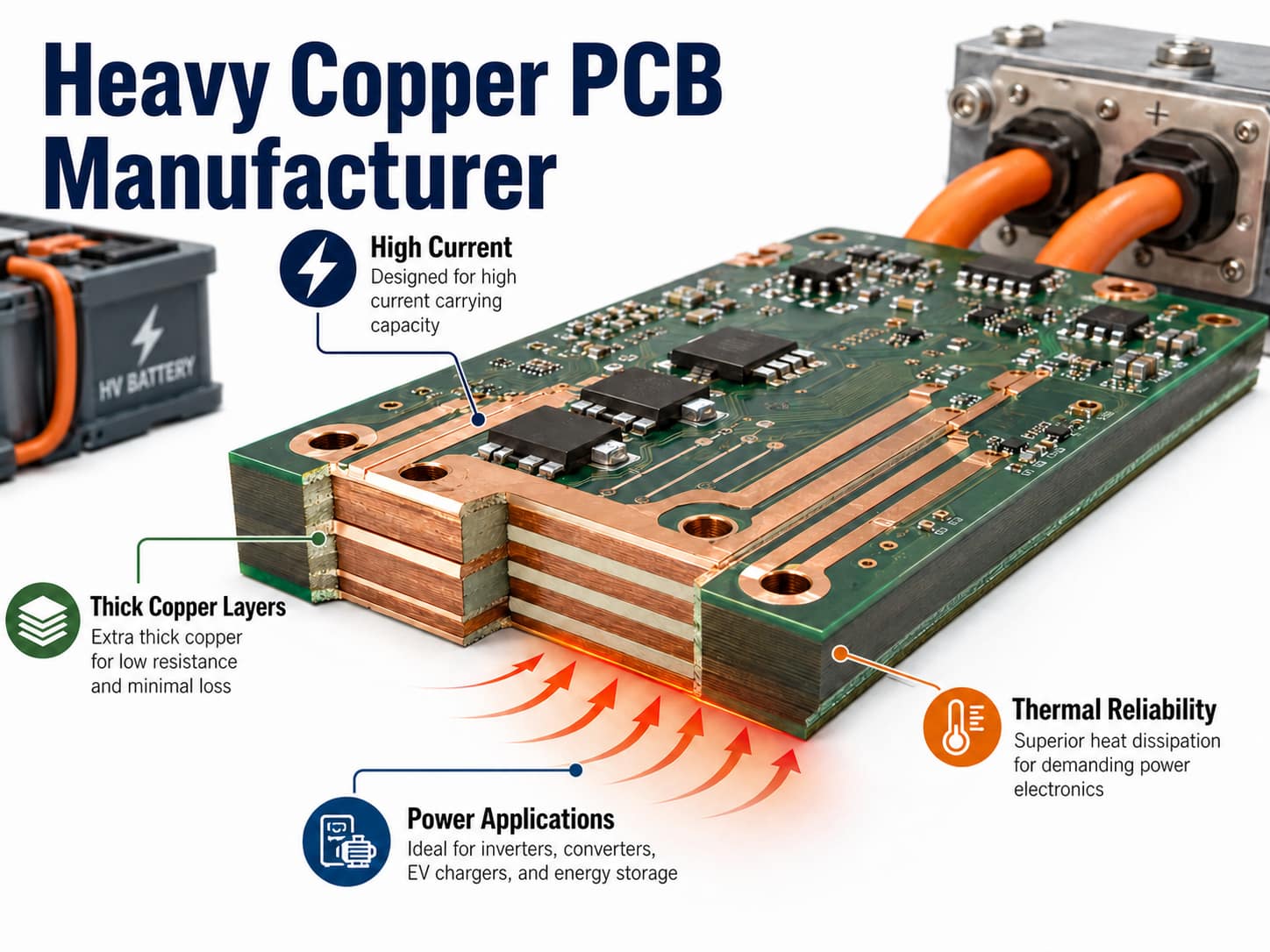
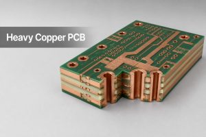
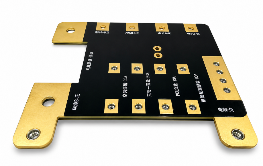
A heavy copper PCB manufacturer builds boards for applications that require higher current capacity, improved heat dissipation, and stronger mechanical reliability than standard copper PCB constructions. By increasing copper thickness on inner or outer layers, these PCBs can support high-power circuits used in battery systems, power converters, industrial equipment, EV charging systems, renewable energy controls, and other demanding electrical applications.
EBest Circuit provides custom heavy copper PCB manufacturing with support for thick copper layers, mixed copper stack-ups, high-current designs, and complex multilayer structures. Our engineering team reviews copper thickness, layer configuration, thermal requirements, via structures, and manufacturing feasibility before production to help customers develop reliable power PCB solutions. Send your Gerber files, stack-up requirements, or application details to sales@bestpcbs.com for engineering review and quotation.
What Maximum Copper Thickness Can Be Achieved for Heavy Copper PCBs?
The maximum copper thickness of a heavy copper PCB depends on the layer position, board size, copper distribution, etching requirements, and manufacturing process capability. Unlike standard PCBs using 1 oz or 2 oz copper, heavy copper designs require specialized processing to maintain copper thickness consistency and reliable circuit formation.
EBest Circuit supports the following verified standard and special-project copper ranges. PCB copper weight must be evaluated with board size, copper distribution, spacing, dielectric fill, and process requirements.
Copper Location
Typical Thickness Capability
Inner layer copper
Standard 0.5–5 oz; special projects 5–20 oz
Outer layer copper
Standard 1–5 oz; special projects 5–20 oz
Mixed copper designs
Available after stack-up and DFM review
100 oz+ request
Project-specific engineering review; not a standard capability
For 100 oz+ copper PCB designs, additional engineering evaluation is required because extremely thick copper affects:
Trace geometry and etching compensation
Copper distribution balance
Lamination pressure and resin filling
Thermal stress during manufacturing
Finished board weight and mechanical strength
Heavy copper capability is not only determined by copper thickness. A reliable manufacturing process must also maintain proper layer alignment, insulation spacing, and plated hole quality.
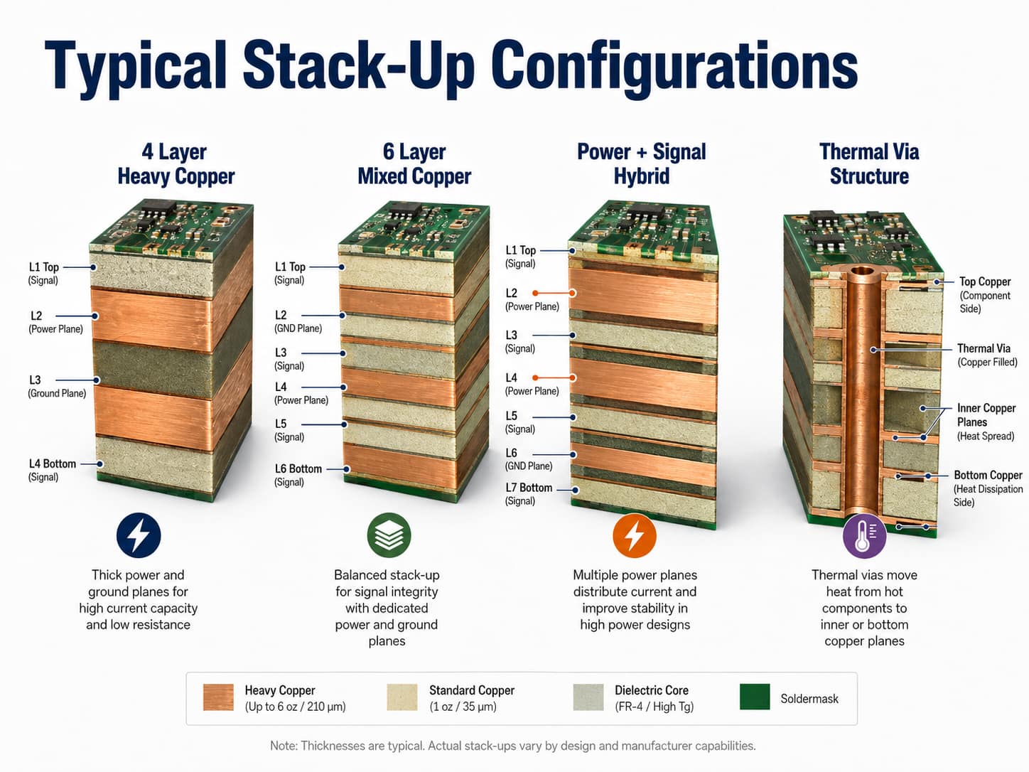
What Heavy Copper PCB Stack-Up Configurations Are Available?
Heavy copper PCBs can be manufactured with different stack-up structures depending on current requirements, thermal performance, signal requirements, and cost targets.
Typical configurations include:
Stack-Up Type
Typical Application
4-layer heavy copper PCB
Power control boards, industrial electronics
6-layer mixed copper PCB
Power and signal integration
Heavy copper outer layers with standard inner layers
High current connection areas
Heavy copper power layers with thermal vias
Heat-sensitive applications
A high current PCB stackup often combines heavy copper layers with standard signal layers. This approach allows engineers to increase current capacity in specific areas without unnecessarily increasing the cost and weight of the entire PCB.
A typical multilayer structure may include:
Thick copper power planes for current distribution
Standard copper signal layers for control circuits
Dedicated thermal layers for heat spreading
Controlled impedance layers when high-speed signals are required
The final stack-up should be reviewed during the engineering stage to ensure copper thickness, dielectric thickness, and manufacturing capability are properly matched.
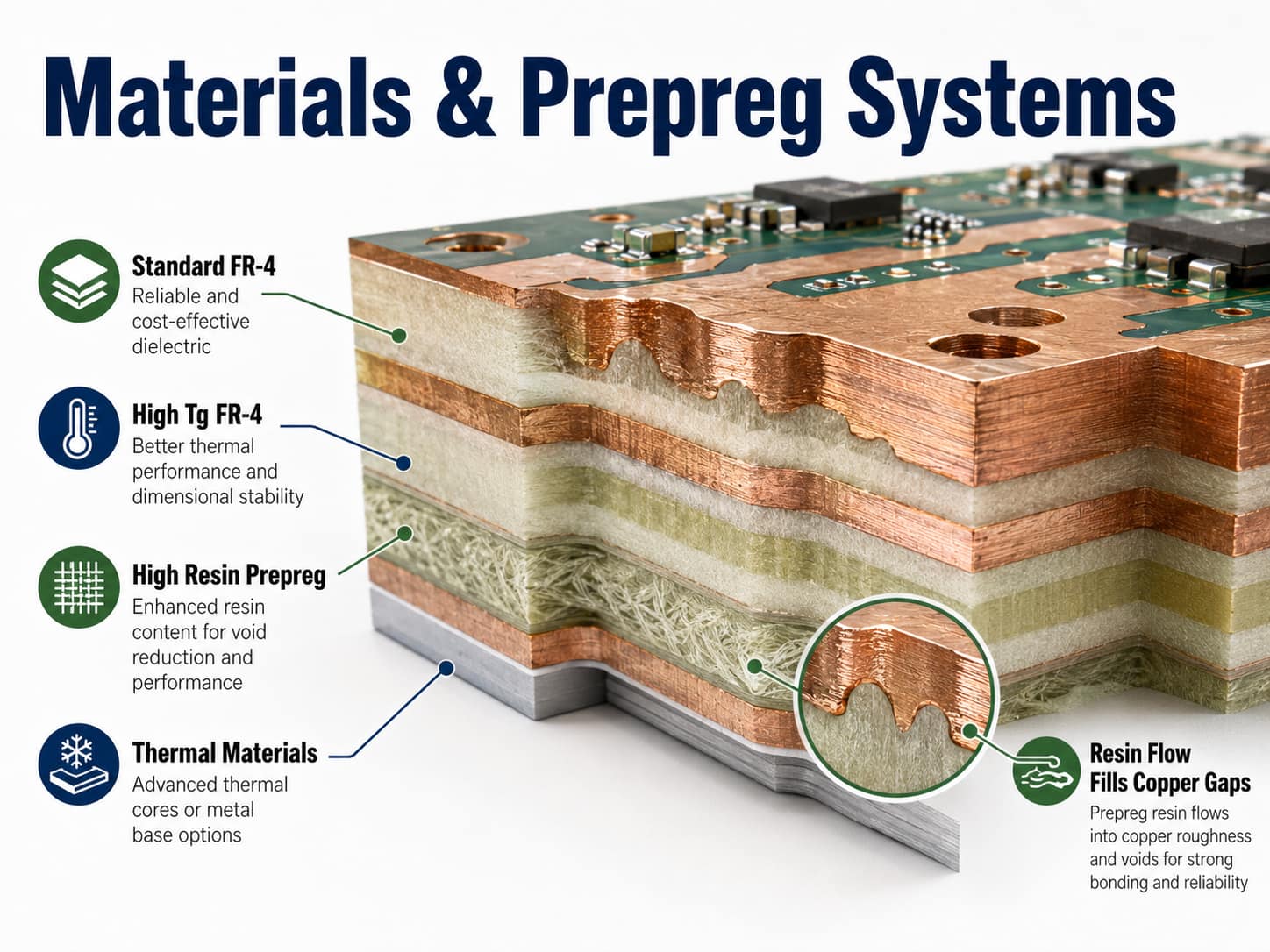
Which Materials and Prepreg Systems Are Used for Heavy Copper PCBs?
Heavy copper PCB materials must provide sufficient mechanical strength, thermal stability, and reliable insulation performance under high current operation.
Common material options include:
Material System
Application Advantage
Standard FR-4
General heavy copper applications
High Tg FR-4
Higher thermal reliability
Thermal management materials
Improved heat dissipation
High resin content prepreg
Better copper gap filling
Prepreg selection is especially important for heavy copper multilayer boards. Thick copper creates larger height differences between copper areas, requiring sufficient resin flow during lamination to prevent voids and ensure reliable insulation.
Material selection depends on:
Operating temperature
Current load
Thermal cycling requirements
Mechanical environment
Industry requirements
For high-power applications, engineers should consider both copper thickness and laminate performance rather than focusing only on copper weight.
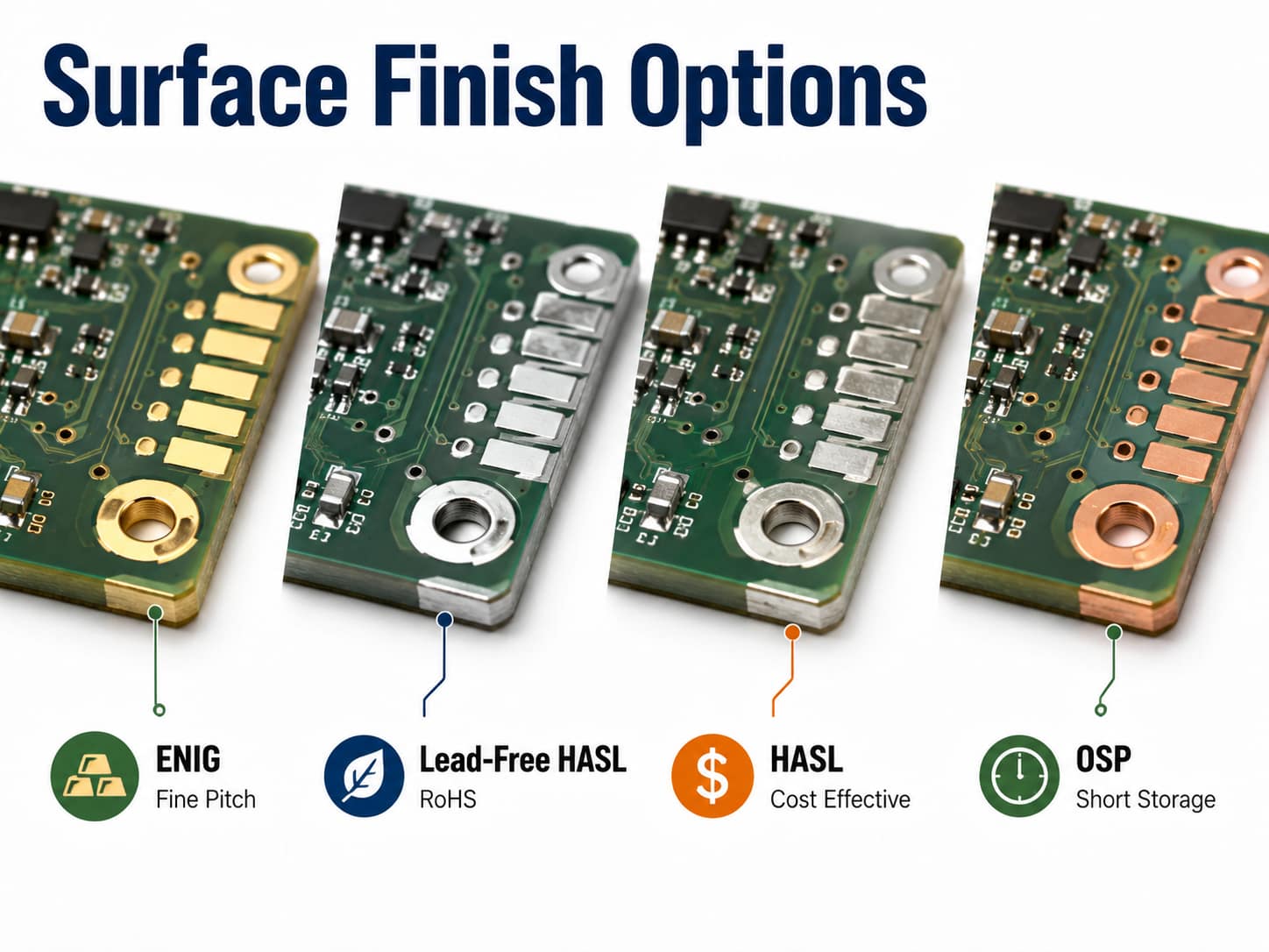
What Surface Finish Options Are Available for Heavy Copper PCBs?
Surface finish selection depends on component requirements, assembly process, reliability expectations, and storage conditions.
Common surface finishes for heavy copper PCBs include:
Surface Finish
Typical Application
ENIG
Fine-pitch components and high reliability applications
Lead-free HASL
Cost-effective industrial applications
HASL
Traditional soldering applications
OSP
Short-term storage and standard assembly
For high-current PCBs, surface finish selection should also consider:
Contact reliability
Solder joint performance
Assembly temperature profile
Long-term environmental exposure
The correct surface finish helps maintain reliable electrical connections throughout the product lifecycle.
What Are the Design Rules and Manufacturing Tolerances for Heavy Copper PCBs?
Heavy copper PCB design requires additional attention compared with standard PCB manufacturing because thicker copper changes trace geometry, spacing requirements, and fabrication conditions.
Important design considerations include:
Design Factor
Engineering Consideration
Trace width and spacing
Requires copper thickness compensation
Copper distribution
Avoid excessive imbalance between layers
Clearance
Must consider thicker copper profiles
Impedance control
Requires stack-up-based calculation
Thermal design
Optimize copper planes and heat paths
During DFM review, engineers typically evaluate:
Copper thickness versus minimum trace width
Etching capability
Layer-to-layer registration
Resin filling conditions
Finished board thickness
These high current PCB design guidelines should be confirmed against the proposed copper weight and stack-up during an engineering DFM review. Early communication helps avoid unnecessary redesign during manufacturing.
Which Via Technologies Are Available for Heavy Copper PCB Manufacturing?
Via structures play an important role in heavy copper PCB performance because they influence current flow, thermal transfer, and mechanical reliability.
Available via technologies include:
Through-hole vias
Plated through vias
Thermal via arrays
Large diameter vias
Multiple parallel vias for current distribution
For power applications, engineers often use multiple thermal vias under heat-generating components or create parallel via paths to reduce electrical resistance.
Via design should consider:
Current requirements
Component heat generation
Copper thickness
Assembly conditions
A proper via structure improves both electrical performance and thermal management.
Which Standards and Certifications Apply to Heavy Copper PCBs?
Heavy copper PCB manufacturing for industrial, automotive, medical, and aerospace applications often requires compliance with recognized quality standards.
Qualification and performance specification for rigid PCBs
IPC-A-600
PCB acceptance criteria
ISO 9001
Quality management system
ISO 13485
Medical device applications
IATF 16949
Automotive applications
AS9100D
Aerospace applications
Specific requirements depend on the final application, customer specifications, and industry regulations.
Quality control processes may include:
Electrical testing
AOI inspection
X-ray inspection when required
Dimensional inspection
Copper thickness verification
What Is the Typical Lead Time for Heavy Copper PCB Production?
Heavy copper PCB lead time depends on copper thickness, layer count, board complexity, testing requirements, and production volume. Review our PCB lead-time guidance as a planning reference; the quotation confirms the actual schedule.
Typical production stages include:
Production Stage
Time Consideration
Engineering review
Based on design complexity
Prototype production
Depends on copper thickness and stack-up
Volume production
Based on quantity and process requirements
Compared with standard PCB production, heavy copper boards may require additional process controls, including:
Special lamination conditions
Copper thickness verification
Additional inspection steps
Manufacturing feasibility review
Providing complete design information during quotation helps shorten engineering evaluation time.
Recommended information includes:
Gerber files
Layer stack-up
Copper thickness requirements
Current load requirements
Application environment
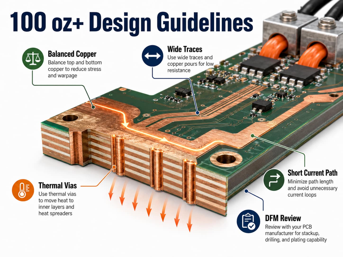
What Design Guidelines Should Be Followed for 100 oz+ Heavy Copper PCBs?
100 oz+ heavy copper PCB requests require project-specific feasibility review because extremely thick copper affects electrical performance, manufacturing processes, and mechanical characteristics. This section provides design inputs for evaluation and does not state an unconditional production capability.
Key design guidelines include:
Optimize copper distribution
Large differences in copper area between layers can create lamination challenges and affect board flatness. Balanced copper distribution improves manufacturing stability.
Consider current path design
High-current paths should use:
Wider copper areas
Shorter current routes
Multiple copper layers when required
Optimized connection points
Plan thermal management early
High-power applications should consider:
Large copper planes
Thermal vias
Heat spreading structures
Component placement strategy
Complete DFM review before production
For 100 oz+ designs, customers should provide:
Maximum current requirement
Operating temperature
Mechanical dimensions
Layer stack-up preference
Reliability requirements
Early engineering review helps confirm whether the design is suitable for production.
Why Choose EBest Circuit for Heavy Copper PCB Manufacturing?
Selecting a heavy copper PCB supplier requires more than checking the maximum copper thickness. Manufacturing experience, engineering support, and process control directly affect final PCB reliability.
EBest Circuit provides:
Heavy copper PCB manufacturing capability
Custom multilayer PCB solutions
Mixed copper stack-up support
Engineering DFM review
Prototype and production support
PCB assembly integration capability
With more than 20 years of PCB manufacturing experience, EBest Circuit supports customers from initial design evaluation through PCB production and PCBA assembly.
For heavy copper PCB projects, contact sales@bestpcbs.com with your Gerber files, copper requirements, or application details.
Frequently Asked Questions About Heavy Copper PCBs
What copper thickness is considered a heavy copper PCB?
Heavy copper PCBs generally refer to boards using copper thickness above standard PCB levels, commonly starting from 3 oz copper and extending to much higher copper weights depending on the application.
Can you manufacture 100 oz copper PCB?
100 oz+ copper PCB requests require project-specific engineering review. Feasibility can be confirmed only after board size, layer structure, copper distribution, insulation, drilling, plating, and reliability requirements are evaluated.
What applications use heavy copper PCBs?
Heavy copper PCBs are commonly used in power supplies, battery systems, EV equipment, industrial controls, renewable energy systems, and high-current electronics.
What materials are recommended for heavy copper PCBs?
High Tg FR-4, suitable prepreg systems, and thermal management materials are commonly selected based on operating temperature and reliability requirements.
Can heavy copper PCBs include controlled impedance designs?
Yes. Controlled impedance can be considered when heavy copper layers are combined with appropriate dielectric thickness and stack-up planning.
What files are needed for heavy copper PCB quotation?
Customers should provide Gerber files, layer stack-up information, copper thickness requirements, board dimensions, quantity, and application details.
Request a Heavy Copper PCB Manufacturing Review
Whether you need a standard heavy copper PCB or want feasibility feedback on a 100 oz+ high-current concept, EBest Circuit can review your design requirements and provide manufacturing recommendations.
Send your PCB files or technical requirements to sales@bestpcbs.com for engineering evaluation and quotation.
A high current PCB must carry large current without excess heat, voltage drop, copper damage, weak solder joints or connector failure. In high-power electronics, the board is part of the current path, heat path and assembly structure.
EBest Circuit provides high-current PCB manufacturing and assembly for motor drivers, inverters, battery systems, power supplies, LED power boards and industrial control modules. From DFM review to heavy copper PCB fabrication, component sourcing, PCBA assembly and testing, EBest helps reduce production risk before batch delivery.
Are you worried about these problems in high-current PCB projects?
Design risk: Wrong trace width, copper thickness, via design or stackup may cause overheating, voltage drop or unstable current output.
Manufacturing risk: Heavy copper etching, drilling, plating and solder mask control may cause weak copper connections, warpage or batch variation.
Assembly risk: Thick copper makes terminals, connectors, busbars and large pads harder to solder and inspect.
EBest Circuit helps reduce these risks before production. Below are our solutions to above problems:
Design review: We check current level, copper thickness, trace width, vias, stackup, spacing and thermal paths before fabrication.
Controlled production: We manage heavy copper etching, drilling, plating, solder mask, surface finish and electrical testing during manufacturing.
Reliable assembly: We support SMT, through-hole assembly, selective soldering, terminal assembly, busbar mounting, heatsink assembly and functional testing.
For high-current PCB manufacturing and assembly projects, send your Gerber files, BOM, stackup, copper thickness and current requirement to EBest Circuit for a quote: sales@bestpcbs.com.
What Is a High Current PCB?
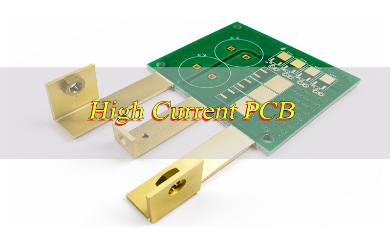
A high current PCB is a printed circuit board designed to carry larger current than a standard signal board or low-power control board. It usually uses wider traces, thicker copper, reinforced vias, large copper planes, high-current connectors and stronger thermal paths.
There is no fixed current value for this board type. A compact 5A power board may already require special review, while a 50A or 100A board may require heavy copper, parallel copper layers or copper busbars.
The main target is safe current carrying with controlled temperature rise and acceptable voltage drop. Current density, copper cross-section, trace length, via quantity, connector rating, solder joint strength and heat dissipation must be reviewed together.
Where Are High Current PCBs Used?
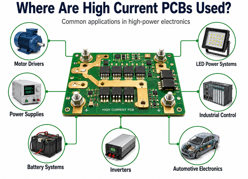
High current PCBs are used in products where the board carries power instead of only signals. These applications often involve switching current, heat, vibration, load change and long service time.
Common applications include:
Motor drivers: BLDC motor control, servo drive, pump control and robotics.
Power supplies: AC-DC modules, DC-DC converters, UPS systems and power distribution.
Battery systems: BMS boards, charging modules, energy storage and battery packs.
Inverters: Solar inverters, industrial inverters and DC-AC power conversion.
Automotive electronics: EV power modules, lighting boards, relay boards and control units.
Industrial control: PLC power modules, actuator control, machinery control and automation equipment.
LED power systems: High-output lighting, LED driver boards and thermal control modules.
These products need stable copper paths, reliable PCBA assembly and controlled thermal performance during long-term use.
How to Choose Copper Thickness for High Current PCB?
Choose copper thickness according to continuous current, allowed temperature rise, trace width, board size, layer count and cost target. Thicker copper increases current capacity, but it also affects etching tolerance, minimum spacing, drilling, solder mask coverage and manufacturing cost.
For many high-power boards, 2 oz or 3 oz copper works well when the layout has wide copper pours and short current paths. For compact boards with higher load, 4 oz, 6 oz or thicker copper may be required.
Very thick copper is not always the best choice. It may create spacing limits, warpage risk or higher production cost, so copper thickness should be reviewed with the stackup and layout.
Copper Weight
Thickness
Typical Use
1 oz
35 µm
Control circuits and low-load power lines
2 oz
70 µm
Moderate power traces and relay boards
3 oz
105 µm
Motor control and power modules
4 oz
140 µm
Heavy copper PCB applications
6 oz
210 µm
High-power distribution boards
10 oz
350 µm
Extreme current and special power systems
A practical selection should combine copper thickness with trace width, high current PCB material, stackup and thermal design.
How to Calculate High Current PCB Trace Width?
High current PCB trace width should be calculated from continuous current, finished copper thickness, allowed temperature rise, trace position and copper length. Do not calculate only by peak current, because short pulse current and long-term working current create different heat levels.
Start with the real working current. For power electronics, use continuous RMS current as the main value, then check surge current separately. If the board works inside a closed enclosure, leave more copper area because heat will be harder to release.
Next, confirm finished copper thickness. A 1 oz copper layer is about 35 µm, 2 oz is about 70 µm, and 3 oz is about 105 µm. Thicker copper can carry more current, but it also affects spacing, etching accuracy and production cost.
Then set an allowed temperature rise, such as 10°C, 20°C or 30°C. A lower temperature rise needs wider copper. External traces usually release heat better than internal traces, so inner-layer current paths need more careful checking.
Finally, check voltage drop and power loss along the trace. A trace may pass the width calculation but still lose too much voltage if it is too long. For important power paths, thermal review and current load testing are recommended before volume production.
What Trace Techniques Improve High Current PCB Reliability?
Reliable high current PCB traces should reduce resistance, spread heat and avoid narrow current bottlenecks. The trace should be treated as a full power path, not just a line in the layout.
Use wider copper pours: Large copper areas reduce resistance and help move heat away from power devices.
Shorten high-current paths: Short copper paths reduce voltage drop, heat generation and power loss.
Avoid neck-down sections: A short narrow area can become the hottest point on the board.
Use parallel copper layers: When one layer is not enough, connect multiple copper layers with enough vias to share current.
Place via arrays near power transfer points: Via arrays lower layer-to-layer resistance and improve heat transfer.
Use smooth copper transitions: Avoid sharp corners and sudden width changes that concentrate current.
Reinforce exposed copper when needed: Controlled solder reinforcement can increase copper cross-section, but solder amount must be controlled.
Use copper busbars for very high current: When PCB copper becomes too wide or costly, busbars can reduce voltage drop and heat.
Keep power paths away from sensitive signals: This reduces noise coupling and improves control circuit stability.
These trace techniques should be checked together with copper thickness, spacing, solder mask opening and assembly process.
How Should Vias Be Designed for High Current PCB?
High current PCB vias must carry current safely between layers. A single small via cannot replace a wide trace or copper plane, so high-current transfer points usually need via arrays, larger holes and sufficient copper plating.
Use multiple vias instead of one via: Several vias share current and reduce local heating.
Increase finished hole size when space allows: Larger holes with proper plating reduce resistance.
Confirm plating thickness: Weak plating can become a failure point under high current or heat cycling.
Keep enough annular ring: A strong pad structure improves drilling tolerance and long-term reliability.
Place vias close to power pads and planes: Shorter transfer paths reduce resistance and heat.
Connect vias to large copper areas: Vias work better when they connect to wide pours or planes, not isolated pads.
Avoid solder wicking near assembly pads: Vias too close to terminals or SMT pads may pull solder away during reflow.
Use thermal vias under power devices: Thermal vias help move heat into inner or bottom copper layers.
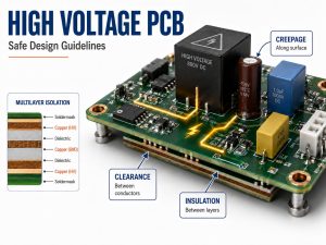
Check via spacing with voltage requirements: High current often appears with higher voltage, so creepage and clearance still matter.
For high-current PCB vias, drilling quality, plating thickness, pad size, copper balance and solderability should be confirmed before production.
How to Design a High Current PCB Stackup?
A high current PCB stackup should support stable current flow, heat spreading, voltage spacing and copper balance. Stackup should be confirmed before final layout because copper weight, dielectric thickness and layer count directly affect routing and production.
Use outer layers for main power copper: Outer copper releases heat more easily and can connect better with heatsinks, terminals or exposed copper areas.
Use inner layers for current sharing: Inner copper planes can reduce voltage drop when connected with enough via arrays.
Keep copper distribution balanced: Heavy copper only on one side may increase bow, twist or lamination stress.
Separate power and signal layers: Keep high-current paths away from control signals to reduce noise.
Check dielectric thickness: Voltage spacing and insulation safety should match the working voltage.
Reserve enough copper spacing: Heavy copper needs larger spacing than standard copper because etching is harder to control.
Plan thermal paths: Heat should move from power devices into copper planes, vias, heatsinks or the enclosure.
The following stackups are common examples. Final layer use should still depend on current level, voltage, heat, EMI, board size and assembly structure.
Example 1: 4-layer high-current PCB stackup Layer 1 can be used for power components and wide current paths. Layer 2 can be a ground or return plane. Layer 3 can be another power or return layer for current sharing. Layer 4 can support low-speed signals, auxiliary power and thermal copper.
Example 2: 6-layer motor driver PCB stackup Layer 1 can hold MOSFETs, terminals and wide copper pours. Layer 2 can act as a return plane. Layer 3 and Layer 4 can share power current through via arrays. Layer 5 can route control signals with shielding from power layers. Layer 6 can be used for bottom copper heat spreading and test access.
A good stackup reduces temperature rise, voltage drop, EMI risk and production deformation.
What Are Best Practices for High Current PCB Layout?
High current PCB layout should keep the power path short, wide, low-resistance and thermally balanced. The layout should also protect control signals from heat and switching noise.
Place power components close to the current path: MOSFETs, diodes, inductors, terminals and connectors should not create long loops.
Avoid copper bottlenecks near connectors: Terminals and connector pads often become hot if copper narrows around them.
Use copper planes and pours: Wide copper areas carry current and spread heat better than thin traces.
Control thermal relief: Excessive thermal relief may make soldering easier but can weaken current capacity.
Separate power and control areas: Keep sensors, MCU signals and feedback traces away from switching current paths.
Use enough vias between current layers: Layer-to-layer current should not pass through only one or two small vias.
Check creepage and clearance: High-current designs may also involve high voltage, so spacing must be safe.
Leave space for assembly and inspection: Terminals, busbars and heatsinks need enough room for soldering and quality checks.
Before fabrication, the layout should be checked for current flow, heat flow, spacing, via reliability and assembly access.
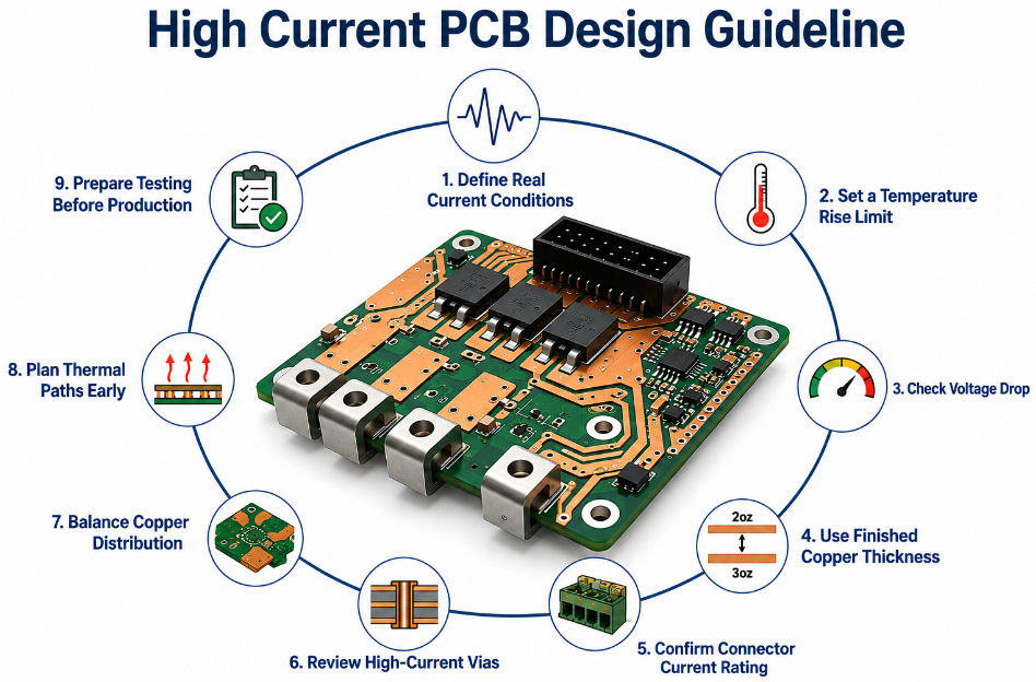
High Current PCB Design Guideline
High current PCB design should combine electrical performance, thermal control and manufacturability. A layout may look correct in CAD but still fail if copper thickness, via plating, connector rating or assembly process is ignored.
Follow these design rules:
Define real current conditions: Separate continuous current, surge current and peak pulse current.
Set a temperature rise limit: Common checks use 10°C, 20°C or 30°C, depending on product requirements.
Check voltage drop: Long copper paths may cause power loss even when the trace width looks acceptable.
Use finished copper thickness: Base copper and finished copper are not always the same after plating and processing.
Confirm connector current rating: A weak connector can fail even when the PCB copper is strong enough.
Review high-current vias: Via count, hole size, plating and pad structure must match the current path.
Balance copper distribution: Uneven heavy copper may cause warpage or lamination stress.
Plan thermal paths early: Copper pours, thermal vias, airflow, heatsinks and enclosure contact should work together.
Prepare testing before production: Current load testing and temperature checks reduce batch risk.
The design goal is safe current flow, stable heat control and repeatable production quality.
How Does Thermal Management Affect High Current PCB Performance?
Thermal management directly affects high current PCB performance because every current path generates heat through resistance. If heat cannot spread or leave the board, copper, laminate, solder joints, connectors and components may age faster.
Good thermal design starts with copper layout. Wider copper, thicker copper, large copper pours and parallel current paths reduce resistance and spread heat. If the current path is narrow at one point, that area may become a hotspot even when the rest of the board looks safe.
Vias also affect heat flow. Thermal vias under MOSFETs, diodes, regulators or power modules can move heat into inner or bottom copper layers. This helps reduce component temperature and protects solder joints from repeated thermal stress.
Material and structure also matter. High-Tg FR-4, metal core structures, heatsinks, thermal pads, airflow and enclosure contact can all improve heat release. The right choice depends on current level, board size, operating temperature and assembly structure.
For high-power electronics, thermal management is part of current capacity, solder joint life, connector reliability and long-term product stability.
What Is the High Current PCB Manufacturing and Assembly Process?
The high current PCB manufacturing and assembly process should control copper quality, solder joint strength and final power performance from the first review to final shipment.
Step 1: Review fabrication and assembly files. Gerber files, drill files, stackup, copper thickness, spacing, solder mask openings, surface finish, BOM, pick and place files, assembly drawings and test requirements should be checked first. This review helps find copper, spacing, via and assembly risks before production.
Step 2: Prepare materials and stackup. The required laminate, copper foil, prepreg and surface finish are confirmed according to current, voltage, heat and assembly needs. For heavy copper boards, copper balance and dielectric spacing should be reviewed before lamination.
Step 3: Manufacture the PCB. Production includes inner layer imaging, heavy copper etching, lamination, drilling, copper plating, outer layer imaging, solder mask, surface finish, routing and electrical testing. For high-current boards, finished copper thickness, plating quality, trace accuracy and copper balance need close control.
Step 4: Assemble components. Assembly includes solder paste control, SMT placement, reflow profiling, through-hole insertion, selective soldering, terminal block assembly, connector soldering, busbar mounting and heatsink installation. Thick copper areas may need adjusted soldering heat to improve solder wetting.
Step 5: Inspect solder joints and current paths. AOI, visual inspection and solder joint review are used to check component placement, solder wetting, terminal joints, connector areas and possible solder defects. Large pads, terminals and busbars should receive closer inspection.
Step 6: Test and pack the finished PCBA. Electrical testing, functional testing, current load testing or temperature rise checking can be arranged according to project requirements. After inspection, the boards are packed for safe shipment.
This process connects high current PCB manufacturing, PCBA assembly and final testing into one controlled production flow.
Why Choose EBest as Your High Current PCB Manufacturer?
Choose EBest when your high current PCB project needs stable current paths, controlled heat, reliable soldering and fewer production delays. EBest combines PCB fabrication, component sourcing and PCBA assembly in one workflow, reducing handoff errors between bare board production and assembly.
Lower design risk: Copper thickness, trace width, via arrays, stackup, spacing, solder mask openings and assembly requirements are reviewed before production.
Faster project progress: PCB prototype, low-volume production, mass production and quick-turn assembly support sample validation and batch delivery.
Better cost control: PCB fabrication, component sourcing and assembly can be reviewed together, reducing repeated quotation changes and BOM delays.
Stronger assembly reliability: SMT, through-hole assembly, mixed assembly, BGA assembly, terminal assembly and connector soldering support complex high-current PCBA projects.
More material choices: Heavy copper PCB, High-Tg PCB, metal core PCB, multilayer PCB, HDI PCB and busbar PCB can support different power electronics designs.
Certified quality support: IATF 16949, ISO 9001, ISO 13485, AS9100D, REACH, RoHS and UL help support high-reliability and compliance-focused projects.
For high-power electronics, EBest helps control design review, manufacturing quality, assembly process and delivery communication in one place.
What High Current PCB Manufacturing and Assembly Services Can EBest Provide?
EBest provides high current PCB manufacturing and assembly services from prototype to mass production.
PCB manufacturing services include:
High current PCB fabrication
Heavy copper PCB manufacturing
High-Tg PCB production
Metal core PCB manufacturing
Multilayer PCB fabrication
HDI PCB manufacturing
Busbar PCB manufacturing
Impedance control PCB
PCB prototype and low-volume production
Mass production
Custom substrate and special material support
PCB assembly services include:
SMT assembly
Through-hole assembly
Mixed assembly
BGA assembly service
Prototype PCB assembly
Quick turn PCB assembly
Full turnkey PCB assembly
Flex PCB assembly
Ceramic PCB assembly
Terminal and connector assembly
Box assembly
Component and process support includes:
Component sourcing
SMD, BGA, QFN and QFP sourcing
Reels, cut tape, tube, tray and loose parts handling
01005 component assembly
0.25mm BGA pitch assembly
SMT/THT mixed assembly
1–5 days assembly lead time depending on project requirements
This service range helps high-current projects move from design files to finished PCBA with fewer sourcing, fabrication and assembly gaps.
How Does EBest Ensure High Current PCB and PCBA Quality?
EBest ensures high current PCB and PCBA quality through front-end review, controlled fabrication, process inspection, assembly verification and final testing. The goal is to prevent weak current paths, poor solder joints, copper defects, overheating and batch inconsistency.
Quality control includes:
DFM review: Copper spacing, copper thickness, drill size, stackup and solder mask are checked before production.
Material control: Laminate, copper foil and solderability are reviewed according to project requirements.
Fabrication inspection: Inner layers, drilling, plating, solder mask and surface finish are monitored during production.
Electrical testing: Open and short testing is applied before shipment.
Assembly inspection: AOI, visual inspection and solder joint review are used after assembly.
Functional testing: Current load, voltage output, temperature rise or project-specific tests can be arranged.
Quality Item
Inspection Focus
Copper thickness
Finished copper and plating consistency
Trace width
Current path and etching accuracy
Vias
Hole quality, plating and solder wicking risk
Solder mask
Opening control and exposed copper protection
Surface finish
Solderability and contact reliability
Assembly
Connector, terminal, busbar and solder joint strength
Testing
Electrical test, functional test and temperature check
For power boards, EBest pays special attention to plating quality, solder filling, connector strength and heat-sensitive areas.
Case Study: Motor Driver PCB Assembly for High-Power Control System
Project background A motor driver PCBA was required for an industrial high-power control system. The board needed to carry large current, drive MOSFET switching, connect to output terminals and operate under long working cycles.
Project requirements
Stable current output for motor control.
Reduced voltage drop across power paths.
Controlled temperature rise around MOSFETs and terminals.
Strong solder joints for connectors, terminals and large pads.
Functional testing before delivery.
Our solution
Power path review: Checked copper width, via arrays, output terminal areas and MOSFET current paths.
Copper structure improvement: Used wider copper pours, parallel current paths and reinforced via arrays to reduce resistance and heat.
Assembly process control: Focused on terminal soldering, connector soldering, large pad wetting and busbar mounting areas.
Inspection and testing: Checked solder joints, current paths, electrical continuity and basic power control performance.
Output result The finished motor driver PCBA had a more stable current path, stronger terminal soldering and better heat distribution around power areas. The project reduced production risk before batch delivery and improved assembly reliability for industrial motor control use.
For similar high-current PCB manufacturing and assembly projects, send Gerber files, BOM, stackup, copper thickness, current requirement and test needs to EBest Circuit for a quote: sales@bestpcbs.com.
What Files Should You Send for a High Current PCB Quote?
To get an accurate high current PCB quote, send complete fabrication and assembly files. Missing copper thickness, stackup, current level or test requirements may cause wrong pricing, repeated questions or production delay.
Required quote files include:
Gerber files
Drill files
PCB stackup
Copper thickness requirement
Board material requirement
Surface finish
Solder mask color
Silkscreen requirement
BOM for assembly
Pick and place file
Assembly drawing
Current rating or load condition
Test requirement
Quantity and delivery target
For high-current projects, also provide continuous current, peak current, operating voltage, ambient temperature, cooling method and any connector, terminal or busbar requirement.
FAQs About High Current PCB Manufacturing and Assembly
Q1: Is FR-4 suitable for high-current power boards? A1: FR-4 can be used when the current, heat and voltage are within safe limits. For higher heat or compact power paths, High-Tg FR-4, metal core PCB or heavy copper PCB may be better. Material choice should match current load, working temperature and product life.
Q2: When should a copper busbar be used instead of only PCB copper? A2: A copper busbar is useful when PCB copper becomes too wide, too hot or too costly. It helps reduce resistance and voltage drop in compact power designs. Busbars are often considered for very high current, limited board space or strong terminal connections.
Q3: Why do terminals and connectors become hot on power PCBs? A3: Terminal heating usually comes from poor contact, undersized copper, weak solder joints or long current paths. Even if the board copper is strong enough, a connector can still overheat. The terminal area should be checked for current rating, pad size, solder wetting and copper support.
Q4: Which surface finish is better for high-current PCB assembly? A4: ENIG, HASL, immersion silver and other finishes can be used, depending on solderability, storage time, contact reliability and cost. For power boards, the surface finish should support strong solder joints, stable connector contact and reliable assembly inspection.
Q5: Why is soldering more difficult on heavy copper PCB? A5: Thick copper absorbs more heat during soldering, so large pads, terminals and busbars may be harder to wet properly. The assembly process may need adjusted reflow profiling, selective soldering, wave soldering or manual solder reinforcement to improve joint strength.
Q6: Can a prototype be changed before mass production? A6: Yes. Prototype production is useful for checking current paths, heat rise, soldering quality and component fit before batch orders. If the prototype shows overheating, voltage drop or soldering issues, the design can be improved before mass production.
Q7: What testing proves a power board can handle current safely? A7: Electrical open/short testing only confirms basic connectivity. For power boards, current load testing and temperature rise checking are more useful. Important checks include voltage drop, terminal temperature, MOSFET area temperature, solder joint condition and output stability.
Q8: What causes voltage drop on a high-current board? A8: Voltage drop often comes from long copper paths, narrow traces, weak via transfer, poor terminal contact or undersized connectors. The issue can be reduced by using wider copper, shorter paths, parallel layers, via arrays and stronger connector areas.
Q9: How can BOM problems delay high-current PCBA projects? A9: Power components, connectors, terminals, MOSFETs, inductors and heatsinks may have long lead times or package changes. A stable sourcing plan helps reduce delays. BOM review should confirm part number, package, current rating, thermal rating and approved alternatives.
Q10: What spacing should be checked on high-current and high-voltage boards? A10: Current capacity and voltage spacing must be checked together. High-current boards often work with higher voltage, so creepage and clearance should match the operating voltage, environment and safety target. Spacing around terminals, slots, busbars and exposed copper should receive extra review.
Q11: What usually increases the cost of a high-current PCB project? A11: Cost usually increases with thicker copper, larger board size, more layers, special material, tighter spacing, busbar mounting, complex assembly and extra testing. Early review helps control cost by balancing copper thickness, trace width, stackup, assembly method and test scope.
Q12: How should finished high-current PCBA be packed for shipment? A12: Heavy components, terminals, connectors and heatsinks can stress solder joints during transport. Finished PCBA should use proper trays, foam, ESD bags or reinforced packaging. The goal is to protect connector areas, large components, solder joints and board edges during shipping.
Q13: What should be checked after receiving high-current PCB assembly? A13: After delivery, check board quantity, surface condition, connector soldering, terminal alignment, heatsink mounting, label information and test records. Before installation, it is also useful to confirm input/output polarity, current rating, mounting holes and mechanical fit.
Q14: Can EBest support urgent high-current PCB and PCBA projects? A14: Yes. EBest supports PCB prototype, low-volume production, mass production, component sourcing and PCB assembly. Depending on project requirements, assembly lead time can be 1–5 days, and urgent PCB boards can be supported with expedited service.
Conclusion
A reliable high current PCB depends on safe current paths, proper copper thickness, strong vias, good thermal control, reliable soldering and final testing. These factors should be reviewed before production, not after defects appear.
EBest Circuit provides high-current PCB manufacturing and assembly from a China-based PCB factory, covering design review, PCB fabrication, component sourcing, PCBA assembly and testing. Send your Gerber files, BOM, stackup, copper thickness and current requirement to us for a quote: sales@bestpcbs.com.
This website uses cookies to enhance your experience, remember your preferences, and help us understand how visitors use our site. You can accept all cookies, reject non-essential cookies, or manage your settings.
This website uses cookies to improve your experience while you navigate through the website. Out of these cookies, the cookies that are categorized as necessary are stored on your browser as they are essential for the working of basic functionalities of the website. We also use third-party cookies that help us analyze and understand how you use this website. These cookies will be stored in your browser only with your consent. You also have the option to opt-out of these cookies. But opting out of some of these cookies may have an effect on your browsing experience.
Necessary cookies are absolutely essential for the website to function properly. These cookies ensure basic functionalities and security features of the website, anonymously.
Cookie
Duration
Description
cookielawinfo-checkbox-analytics
11 months
This cookie is set by GDPR Cookie Consent plugin. The cookie is used to store the user consent for the cookies in the category "Analytics".
cookielawinfo-checkbox-functional
11 months
The cookie is set by GDPR cookie consent to record the user consent for the cookies in the category "Functional".
cookielawinfo-checkbox-necessary
11 months
This cookie is set by GDPR Cookie Consent plugin. The cookies is used to store the user consent for the cookies in the category "Necessary".
cookielawinfo-checkbox-others
11 months
This cookie is set by GDPR Cookie Consent plugin. The cookie is used to store the user consent for the cookies in the category "Other.
cookielawinfo-checkbox-performance
11 months
This cookie is set by GDPR Cookie Consent plugin. The cookie is used to store the user consent for the cookies in the category "Performance".
viewed_cookie_policy
11 months
The cookie is set by the GDPR Cookie Consent plugin and is used to store whether or not user has consented to the use of cookies. It does not store any personal data.
Functional cookies help to perform certain functionalities like sharing the content of the website on social media platforms, collect feedbacks, and other third-party features.
Performance cookies are used to understand and analyze the key performance indexes of the website which helps in delivering a better user experience for the visitors.
Analytical cookies are used to understand how visitors interact with the website. These cookies help provide information on metrics the number of visitors, bounce rate, traffic source, etc.
Advertisement cookies are used to provide visitors with relevant ads and marketing campaigns. These cookies track visitors across websites and collect information to provide customized ads.