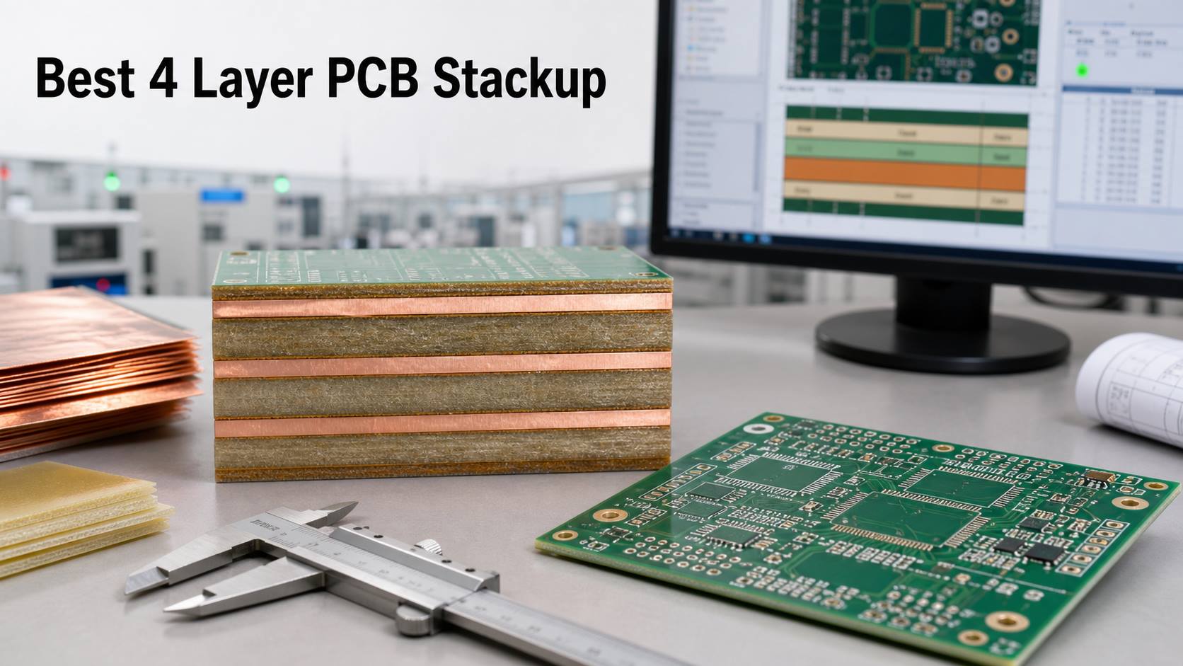
Best 4 layer PCB stackup is not a fixed layer order for every project. It is the stackup that helps a 4 layer PCB achieve stable routing, clean power distribution, EMI control, manufacturable spacing, and reliable assembly when a 2 layer board is no longer enough.
The right stackup depends on signal speed, board thickness, copper thickness, material, impedance, power distribution, component density, cost, lead time, and assembly needs. EBest Circuit (Best Technology) supports custom 4 layer PCB manufacturing, stackup review, DFM checking, controlled impedance production, component sourcing, and PCBA assembly. If you are preparing a 4 layer PCB project, pls feel free to send your Gerber data or ODB++ files, fabrication drawing, stackup notes, Readme file, technical specifications, impedance requirements, board thickness, and copper thickness to sales@bestpcbs.com for engineering review before production. If 4 layer PCB assembly is also required, please include the BOM and assembly files.
What Is the Best 4 Layer PCB Stackup?
The best 4 layer PCB stackup is the structure that gives your board stable routing, clean return paths, manufacturable spacing, reliable power delivery, and reasonable cost.
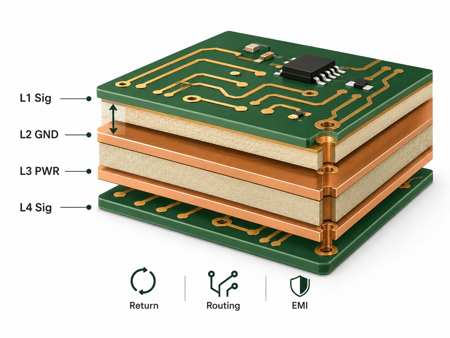
A common 4 layer PCB stackup is:
| Layer | Function |
|---|---|
| L1 | Signal |
| L2 | Ground plane |
| L3 | Power plane |
| L4 | Signal |
This structure is widely used because the ground plane on L2 gives top-layer signals a close reference plane. It helps reduce loop area, improve return current paths, and support better EMI control than a 2 layer PCB.
But there is no single best stackup for every board. A good stackup should be decided based on:
- Signal type and routing speed
- Total finished board thickness
- Inner and outer copper thickness
- Material and Tg requirement
- Impedance control
- EMI/EMC concerns
- Thermal performance
- Cost target
- Testing and assembly needs
In PCB manufacturing, stackup is not just a theoretical layer order. It must match real materials, lamination behavior, copper balance, drill capability, solder mask process, and final board thickness tolerance.
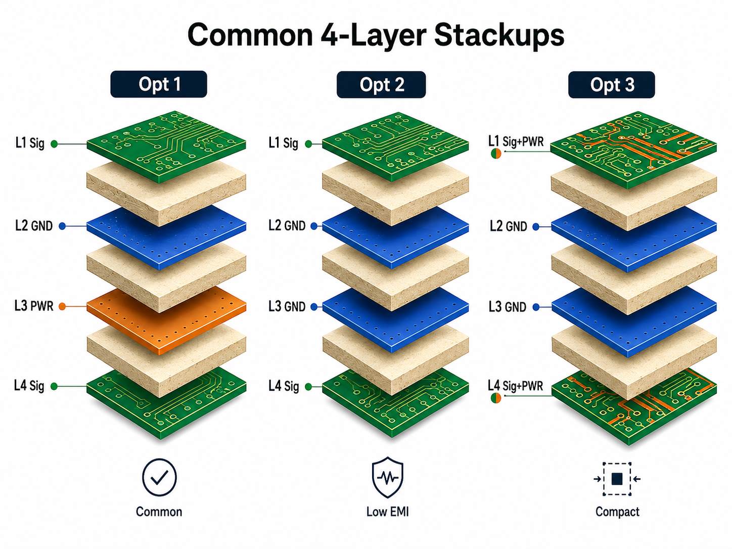
Common 4 Layer PCB Stackup Structures
Most 4 layer PCB stackups use two outer signal layers and two internal reference layers. The right structure depends on the circuit and manufacturing goal.
Option 1: Signal / Ground / Power / Signal
| Layer | Use |
| L1 | Components and signals |
| L2 | Ground plane |
| L3 | Power plane |
| L4 | Signals |
This is the most common 4 layer PCB stackup. It works well for industrial control boards, sensor boards, IoT boards, communication modules, and many embedded products.
Option 2: Signal / Ground / Ground / Signal
| Layer | Use |
| L1 | Signals |
| L2 | Ground |
| L3 | Ground |
| L4 | Signals |
This structure can be useful when EMI control, signal return path, or noise reduction is more important than a dedicated power plane. Power must be routed with wider traces or copper pours.
Option 3: Signal + Power / Ground / Ground / Signal + Power
This option is useful when the board has limited power complexity but needs stronger grounding. It can work for some compact boards, but the power routing must be checked carefully.
Before production, the manufacturer should confirm the stackup with real Core, Prepreg, copper foil, board thickness, and impedance requirements. A stackup that looks simple in CAD can still create manufacturing risk if the material structure is not realistic.
Best 4 Layer PCB Stackup for Signal and Power Integrity
For signal integrity, the most important rule is that high-speed signals need a stable return path. In many 4 layer boards, this means placing a continuous ground plane close to the signal layer.
If L1 carries high-speed traces, L2 should normally be a solid ground plane. This gives signals a short return path and helps reduce noise and radiation.
For power integrity, the stackup should support stable voltage delivery to ICs, connectors, sensors, communication chips, and power circuits. The board should allow:
- Short decoupling paths
- Enough copper area for current
- Stable ground reference
- Clean power-to-ground connection
- Practical power routing
- Controlled copper balance
A practical selection can look like this:
| Project Need | Stackup Focus |
| General embedded control | L2 ground, L3 power |
| High-speed signal routing | Close ground reference |
| Noise-sensitive analog | Clean ground and separated routing zones |
| Power control board | Copper weight and thermal path |
| Compact product | Trace/space, via, and panel feasibility |
The best 4 layer PCB stackup is not always the most complex one. It is the stackup that supports the product with fewer layout compromises and fewer manufacturing problems.
4 Layer PCB Stackup for Controlled Impedance
If the board uses USB, Ethernet, LVDS, MIPI, high-speed clocks, RF traces, or other controlled signal paths, the 4 layer PCB stackup must be reviewed for impedance.
Controlled impedance is affected by:
- Trace width
- Trace spacing
- Copper thickness
- Dielectric thickness
- Reference plane
- Solder mask
- Material type
- Finished board thickness
For example, a 50 ohm single-ended trace on L1 will usually reference L2. A 90 ohm or 100 ohm differential pair also needs a clear reference plane and stable dielectric thickness.
A practical impedance request should include:
| Item | Why It Matters |
| Target impedance | 50 ohm, 90 ohm, 100 ohm, etc. |
| Signal layer | Defines routing location |
| Reference layer | Affects impedance calculation |
| Trace width and spacing | Needed for production control |
| Tolerance | Defines acceptable result |
| Report requirement | Confirms test documentation |
EBest Circuit can support controlled impedance review and provide impedance reports when required. For engineers, this is especially important before production or when the PCB connects to high-speed modules, connectors, or communication interfaces.
Best 4 Layer PCB Stackup for High-Speed Boards
A 4 layer PCB can support many high-speed boards, but the stackup must be planned carefully.
A practical high-speed 4 layer PCB stackup often uses:
| Layer | Function |
| L1 | High-speed signals and components |
| L2 | Solid ground plane |
| L3 | Power plane or ground/power layer |
| L4 | Slower signals or secondary routing |
This keeps the top signal layer close to ground. It is often better than routing high-speed signals far away from a reference plane.
For high-speed boards, engineers should also check:
- Differential pair routing
- Via transitions
- Return path continuity
- Connector breakout
- BGA escape routing
- Crosstalk spacing
- Decoupling capacitor placement
- Impedance coupon requirement
A 4 layer board has limits. If the product has dense BGA, multiple high-speed interfaces, many power rails, or strict EMI requirements, a 6 layer PCB may be more practical.
4 Layer PCB Stackup vs 2 Layer and 6 Layer PCB
A 4 layer PCB sits between simple 2 layer boards and more complex 6 layer boards.
| PCB Type | Best For | Limitation |
| 2 layer PCB | Simple circuits and low-cost prototypes | Limited routing and weaker EMI control |
| 4 layer PCB | Better signal integrity, power distribution, and compact routing | Limited routing and plane flexibility |
| 6 layer PCB | More high-speed routing and better power/ground planning | Higher cost than 4 layers |
A 2 layer PCB may be enough for simple LED boards, basic control boards, or low-speed products. But when the board has more ICs, connectors, communication lines, or EMI concerns, 4 layers often become the better choice.
A 6 layer PCB may be needed when the design has:
- Dense BGA components
- Multiple high-speed interfaces
- More power rails
- Strict impedance requirements
- Complex grounding needs
- Tight mechanical constraints
For many engineering projects, 4 layers offer a strong balance between cost and performance.
4 Layer PCB Manufacturing Rules That Affect Stackup
A stackup must match real PCB manufacturing rules. It is not only an electrical decision.
Customer files should be reviewed first
A reliable PCB manufacturer should review more than Gerber files. Useful customer information may include:
- Gerber or ODB++ data
- Fabrication drawing
- Readme file
- Stackup drawing
- Copper thickness requirement
- Board thickness and tolerance
- Impedance notes
- Material requirement
- Surface finish
- Assembly notes
- General specification
If these details are unclear, the manufacturer should raise EQ before production.
Core, Prepreg, and copper foil matter
A 4 layer PCB stackup is built with Core, Prepreg, and copper foil.
- Core: cured laminate with copper on both sides
- Prepreg / PP: semi-cured material used for lamination
- Copper foil: conductive copper layer, such as 18um, 35um, or 70um
A common copper reference is:
| Copper | Approximate Thickness |
| 0.5oz | 18um |
| 1oz | 35um |
| 2oz | 70um |
Prepreg becomes thinner after lamination, and resin flow must be considered. This matters more when the board uses heavier copper.
Copper balance affects warpage
- Copper distribution should be reviewed across layers. If copper area is very different between layers, the finished PCB may have higher warpage risk. For heavy copper boards, copper balance and lamination structure become especially important.
2oz copper needs more process review
When copper thickness reaches 2oz or above, the manufacturer should check:
- Etching compensation
- Minimum trace/space
- Resin filling between copper areas
- Prepreg selection
- Lamination risk
- Solder mask coverage
- Board thickness control
- Copper balance
For 4 layer PCB projects, these manufacturing details can affect yield, lead time, and final reliability.
4 Layer PCB Cost, Lead Time, and Material Options
The cost of a 4 layer PCB depends on more than the layer count.
Common cost factors include:
- Board size
- Quantity
- Material type
- Board thickness
- Copper thickness
- Minimum trace/space
- Minimum hole size
- Surface finish
- Impedance control
- Testing requirements
- PCBA assembly
- Component sourcing
- Delivery schedule
Material availability also affects lead time. Many PCB manufacturers keep standard Core, Prepreg, FR4 laminate, and copper foil in stock to shorten delivery. If a customer requires non-standard material, special Tg, unusual thickness, or uncommon Prepreg combination, the manufacturer should confirm availability before promising lead time.
Common material choices include:
| Material Option | Typical Use |
| FR4 Tg130 | Standard commercial boards |
| FR4 Tg150 | Better thermal reliability |
| FR4 Tg170 | Higher reliability or thermal demand |
| High-speed material | Signal-sensitive applications |
| Heavy copper | Higher current or thermal needs |
For prototype projects, speed and DFM feedback are often more important than only chasing the lowest price. For production projects, repeatability, documentation, and stable quality control become more important.
How to Choose a 4 Layer PCB Manufacturer in China
When choosing a 4 layer PCB manufacturer in China, do not only compare online prices. A good supplier should understand both stackup and manufacturing.
A practical supplier should be able to:
- Review Gerber, drawing, Readme, and stackup notes
- Confirm board thickness and copper thickness
- Check impedance feasibility
- Review Core and Prepreg selection
- Evaluate copper balance and warpage risk
- Support prototype and small batch production
- Provide PCB fabrication and PCBA assembly together
- Raise EQ before production when details are unclear
- Provide reports when required
For international buyers, communication is important. A good 4 layer PCB manufacturer should not silently guess. They should confirm unclear stackup, impedance, material, panelization, or assembly details before production.
Why Choose EBest Circuit for 4 Layer PCB Stackup and Manufacturing?
EBest Circuit (Best Technology) supports custom 4 layer PCB manufacturing for prototype, small batch, and production projects. For engineers, our value is not only building the PCB, but helping check whether the board is ready for reliable manufacturing and assembly.
What EBest Circuit supports
- 4 layer FR4 PCB manufacturing
- Stackup and DFM review before production
- Controlled impedance PCB manufacturing
- PCB prototype and small-batch production
- Component sourcing and BOM support
- PCB SMT assembly and PCBA testing
- Surface finishes such as ENIG, HASL, OSP, and others based on project needs
- Engineering review for board thickness, copper thickness, via structure, material, and panelization
Why it matters
- A wrong stackup can affect impedance and EMI.
- Poor copper planning can affect power stability.
- Heavy copper needs lamination and solder mask review.
- Unclear customer files can delay production.
- Separate PCB and SMT suppliers can miss assembly notes.
- Incomplete documentation can slow validation.
EBest Circuit has over 20 years of PCB and PCBA experience, with support for PCB fabrication, component sourcing, PCBA assembly, testing, and engineering review. We hold quality certifications including ISO9001, ISO13485, IATF16949, and AS9100D, and support traceability through digital production management.
4 Layer PCB Stackup Manufacturing Case Study
A European industrial electronics customer needed a 4 layer FR4 PCB for a power control module used in factory equipment. The board was not an HDI project, but it had one important manufacturing requirement: 2oz copper on both inner and outer layers.
Project snapshot
- Customer: Europe
- Application: Industrial power control module
- Board type: 4L FR4 PCB
- Material: FR4 Tg130
- Copper thickness: 2oz inner and outer copper
- Finished thickness: 1.6mm +/-10%
- Surface finish: ENIG, Au 1u”
- Solder mask / silkscreen: Green solder mask, white silkscreen
- Main focus: Stackup feasibility, copper spacing, lamination quality, and thickness control
Main challenge
Compared with a standard 1oz 4 layer PCB, 2oz copper changes the manufacturing risk. It affects etching, trace spacing, resin filling, copper balance, solder mask coverage, lamination thickness, and cost.
For this project, the stackup could not be checked only by layer order. The engineering team needed to confirm whether the selected structure could support 2oz copper while keeping the finished board at 1.6mm +/-10%.
EBest Circuit solution
- Reviewed the 4 layer PCB stackup before production
- Checked whether 2oz copper matched the required trace/space
- Reviewed Prepreg resin filling for heavier copper areas
- Checked copper balance to reduce warpage risk
- Confirmed finished thickness control at 1.6mm +/-10%
- Reviewed solder mask coverage over heavy copper
- Confirmed ENIG Au 1u” for solderability and contact reliability
- Provided DFM feedback before fabrication
Customer value
For this customer, the value was not only getting a 4 layer PCB manufactured. EBest Circuit helped check whether the stackup could support 2oz copper, 1.6mm thickness, ENIG finish, and stable production yield before manufacturing started.
This reduced avoidable production risks and made the board more suitable for industrial power control use.
FAQs about Best 4 Layer PCB Stackup
1. What is the best 4 layer PCB stackup?
A common best 4 layer PCB stackup is Signal / Ground / Power / Signal. It works well for many embedded, industrial, and communication boards because it gives top-layer signals a close ground reference and supports better power distribution than a 2 layer PCB.
2. Can a 4 layer PCB support controlled impedance?
Yes. A 4 layer PCB can support controlled impedance if the stackup, dielectric thickness, copper thickness, trace width, spacing, and reference plane are properly defined before manufacturing.
3. Is 2oz copper suitable for a 4 layer PCB?
Yes, but it needs manufacturing review. 2oz copper affects etching, spacing, resin filling, solder mask coverage, board thickness, and copper balance. The stackup should be checked before production.
4. When should I choose a 6 layer PCB instead of a 4 layer PCB?
Choose 6 layers when the board has dense BGA, multiple high-speed interfaces, many power rails, strict EMI requirements, or routing that becomes too difficult on 4 layers.
5. How do I choose a 4 layer PCB manufacturer in China?
Choose a manufacturer that can review stackup, support impedance control, provide DFM feedback, handle PCB and PCBA together, source components if needed, and confirm unclear requirements before production.
In short, If you are not sure which 4 layer PCB stackup is right for your project, send your Gerber data or ODB++ files, fabrication drawing, stackup notes, Readme file, technical specifications, impedance requirements, board thickness, copper thickness, and acceptance requirements to sales@bestpcbs.com. If PCBA is also required, please include the BOM and assembly files. EBest Circuit’s engineering team can review the stackup and manufacturing path before production.