In an era of global supply chain uncertainties, us based pcb manufacturers specializing in industrial PCB manufacturing have emerged as a strategic choice for businesses across sectors. Unlike overseas suppliers, us based pcb manufacturers prioritize compliance with strict industrial standards (such as MIL-PRF and ISO 9001), ensuring that every circuit board meets the reliability requirements of critical applications. The core value of partnering with us based pcb manufacturers for local industrial PCB manufacturing lies in reduced lead times, eliminated tariff risks, and direct access to engineering support—factors that minimize project delays and enhance product performance. Whether you’re developing aerospace components or medical devices, collaborating with us based pcb manufacturers for your industrial PCB manufacturing needs delivers peace of mind, knowing your products are built to withstand rigorous industrial demands.
Choose Our US Based PCB Manufacturing – Solve Your Industrial PCB Manufacturing Pain Points
Tired of navigating the frustrations of offshore industrial PCB manufacturing? Our team of us based pcb manufacturers is designed to address the key challenges that hinder your projects. We offer flexible order quantities with no minimum requirements, solving the common issue of overseas suppliers refusing small-batch industrial PCB orders. Our local production eliminates import tariffs and reduces shipping times from weeks to days, cutting down on hidden costs and delays. With 30 years of expertise in industrial PCB manufacturing, our engineers provide 24/7 technical support to refine your designs—no language barriers or time zone gaps. As trusted us based pcb manufacturers, we hold UL and ISO 13485 certifications, guaranteeing compliance for medical, automotive, and aerospace applications. Skip the supply chain headaches: choose our us based pcb manufacturers and get high-quality, on-time PCBs tailored to your industrial needs.
Key Capabilities of Top US Based PCB Manufacturers
Top us based pcb manufacturers distinguish themselves through versatile capabilities that cater to diverse industrial demands. Here’s what sets leading providers apart:
Full Range of PCB Types for Industrial Applications
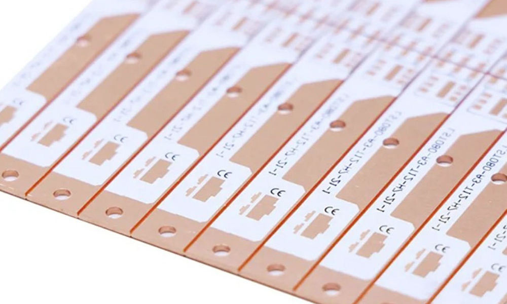
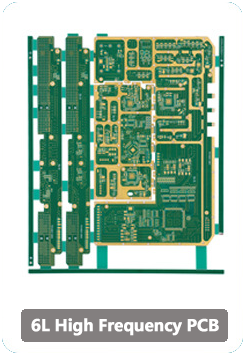
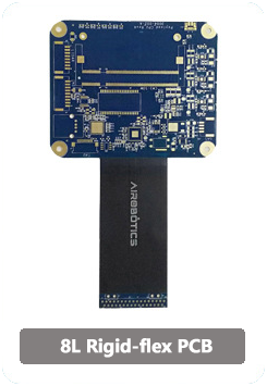
From rigid FR-4 boards to flexible and rigid-flex PCBs, us based pcb manufacturers offer comprehensive solutions. We specialize in high-density interconnect (HDI) boards for compact industrial devices, aluminum-backed PCBs for thermal management in power electronics, and RF/microwave PCBs for communication equipment. Our production line handles boards up to 50 layers, supporting the complex circuitry required for industrial automation and IoT devices.
Advanced Manufacturing Technologies
Leading us based pcb manufacturers invest in state-of-the-art equipment, including automated optical inspection (AOI) systems, laser direct imaging (LDI) machines, and X-ray inspection tools. These technologies ensure precision in soldering, trace alignment, and component placement—critical for industrial PCBs that operate in harsh environments (extreme temperatures, vibration, or chemical exposure).
How to Select Reliable US Based PCB Manufacturers
Choosing the right us based pcb manufacturers for your industrial PCB manufacturing project requires careful evaluation. Follow these actionable steps to identify a trustworthy partner:
Verify Certifications and Compliance
Reliable us based pcb manufacturers hold industry-recognized certifications: UL for safety, ISO 9001 for quality management, and AS9100 for aerospace/defense applications. Ask for documentation to confirm compliance with your industry’s specific standards (e.g., IATF 16949 for automotive, ISO 13485 for medical).
Evaluate Production Capacity and Lead Times
Inquire about minimum order quantities (MOQs), maximum production volume, and typical lead times. The best us based pcb manufacturers offer flexibility—accommodating both small-batch prototypes (1-100 units) and large-scale production runs (10,000+ units) with quick turnaround (1-5 days for prototypes, 2-3 weeks for mass production).
Check Customer References and Case Studies
Reputable us based pcb manufacturers will share references from industrial clients in your sector. Look for case studies that highlight successful projects, such as reducing downtime for a manufacturing plant or meeting strict deadlines for a defense contract.
Quick-Turn Prototype Services from US Based PCB Manufacturers
For industrial innovators and startups, quick-turn prototypes are make-or-break for product development—and us based pcb manufacturers excel in this area. Our rapid prototyping service delivers functional industrial PCB samples in 1-3 business days, allowing you to test designs, identify flaws, and iterate fast.
Materials and Specifications for Prototype PCBs
We use industry-standard materials (FR-4, Rogers 4350B, polyimide) for prototypes, ensuring consistency with mass production. You can customize trace widths, hole sizes, and surface finishes (HASL, ENIG, OSP) to match your final product requirements. As us based pcb manufacturers, we source materials locally, avoiding delays from international shipping.
Benefits of Local Quick-Turn Prototyping
Working with us based pcb manufacturers for prototypes means you can collaborate directly with engineers to resolve design issues in real time. No more waiting for overseas suppliers to respond—our team provides same-day feedback, helping you stay on schedule for product launches or investor demos.
High-Volume Production Solutions by US Based PCB Manufacturers
When your industrial product moves to scale, us based pcb manufacturers offer the stability and efficiency needed for high-volume industrial PCB manufacturing. Our automated production lines (equipped with SMT placement machines and wave soldering systems) handle 10,000+ units per run with consistent quality.
Cost Savings for Bulk Orders
As us based pcb manufacturers, we pass on economies of scale to clients: bulk orders qualify for volume discounts, and local production eliminates import tariffs and long shipping costs. We also offer inventory management services, storing excess PCBs and delivering them just-in-time to reduce your storage expenses.
Quality Control for High-Volume Runs
Every batch of industrial PCBs undergoes 100% AOI inspection and random X-ray testing to ensure zero defects. Our quality control team follows Six Sigma principles, maintaining a defect rate of less than 0.001%—a standard that many overseas suppliers can’t match.
Industry-Specific PCB Solutions from US Based PCB Manufacturers
Us based pcb manufacturers understand that industrial sectors have unique requirements—and we tailor our solutions accordingly:
Aerospace and Defense PCBs
We produce PCBs that meet MIL-PRF-55110 and AS9100 standards, with features like radiation hardening, flame retardancy, and resistance to extreme temperatures. Our aerospace clients rely on us for mission-critical components in satellites, drones, and military vehicles.
Medical Device PCBs
Compliant with ISO 13485 and FDA regulations, our medical PCBs are used in diagnostic equipment, implantable devices, and surgical tools. We prioritize biocompatibility, sterilization resistance, and low electromagnetic interference (EMI) to ensure patient safety.
Automotive Electronics PCBs
For electric vehicles (EVs) and autonomous driving systems, we manufacture PCBs that withstand high voltage, vibration, and temperature fluctuations. Our automotive PCBs meet IATF 16949 standards and support features like battery management, infotainment, and sensor integration.
Quality Certifications That Matter for US Based PCB Manufacturers
Certifications are non-negotiable for us based pcb manufacturers serving industrial clients—they prove our commitment to quality and compliance:
UL Certification
UL certification ensures our PCBs meet safety standards for flammability and electrical performance, a requirement for products sold in the US and Canada.
ISO 9001:2015
This certification validates our quality management system, ensuring consistent processes from design to delivery.
AS9100D
Specific to aerospace and defense, AS9100D demonstrates our ability to meet the strict quality requirements of these high-stakes industries.
ISO 13485
For medical device manufacturers, ISO 13485 certification confirms our adherence to medical industry quality standards.
Cost Factors to Consider When Working with US Based PCB Manufacturers
While us based pcb manufacturers may have slightly higher upfront costs than overseas suppliers, the total cost of ownership (TCO) is often lower. Here’s what impacts pricing:
PCB Design Complexity
Factors like layer count (2-50+), trace density, and hole size affect production time and material usage. Our engineers can suggest design optimizations (e.g., reducing unnecessary layers) to lower costs without compromising performance.
Material Selection
Standard materials like FR-4 are more cost-effective, while specialty materials (e.g., Rogers for high-frequency applications) come at a premium. We help you balance performance needs with budget constraints.
Order Quantity and Lead Time
Small-batch orders or expedited lead times (1-2 days) may incur higher per-unit costs. Planning ahead and ordering in bulk can significantly reduce expenses.
Lead Time & Delivery Expectations for US Based PCB Manufacturers
One of the biggest advantages of us based pcb manufacturers is fast, reliable delivery:
Typical Lead Times
- Prototypes: 1-3 business days (quick-turn option: 24-48 hours)
- Medium-volume orders (100-1,000 units): 5-7 business days
- High-volume orders (1,000+ units): 2-3 weeks
Shipping and Logistics
We partner with USPS, UPS, and FedEx for domestic delivery, with most orders arriving within 1-3 days of production completion. For urgent projects, we offer same-day shipping from our facilities in California, Texas, and Ohio. Unlike overseas suppliers, we provide real-time tracking and full transparency throughout the shipping process.
FAQ – Common Questions About US Based PCB Manufacturers
1. What types of industrial PCBs do US based pcb manufacturers produce?
Us based pcb manufacturers produce a wide range, including rigid, flexible, rigid-flex, HDI, aluminum-backed, and RF/microwave PCBs. We cater to aerospace, medical, automotive, industrial automation, and telecommunications sectors.
2. Are US based pcb manufacturers more expensive than overseas suppliers?
While upfront costs may be 10-20% higher, us based pcb manufacturers eliminate tariffs (up to 25% for Chinese imports), reduce shipping costs, and avoid delays—lowering your total cost of ownership. The added value of quality, compliance, and technical support often justifies the difference.
3. Can US based pcb manufacturers handle small-batch prototype orders?
Yes—most us based pcb manufacturers offer no-minimum order quantities, with quick-turn prototype services for 1-100 units. This is ideal for startups and engineers testing new designs.
4. What certifications should I look for in US based pcb manufacturers?
Prioritize UL, ISO 9001, and industry-specific certifications (AS9100 for aerospace, ISO 13485 for medical, IATF 16949 for automotive). These ensure compliance with safety and quality standards.
5. How long does it take to receive PCBs from US based pcb manufacturers?
Prototypes take 1-3 days, medium-volume orders 5-7 days, and high-volume orders 2-3 weeks. Expedited options are available for urgent projects.
6. Do US based pcb manufacturers offer design support?
Yes—our engineering team provides free design for manufacturing (DFM) reviews, helping you optimize your PCB layout for production, reduce costs, and avoid delays.
7. Are US based pcb manufacturers compliant with environmental regulations?
Absolutely—us based pcb manufacturers follow RoHS, REACH, and California Prop 65 regulations, ensuring our PCBs are free of hazardous substances.
8. Can US based pcb manufacturers handle high-temperature or harsh-environment PCBs?
Yes—we specialize in PCBs for extreme conditions, using materials like polyimide (flexible) and Rogers (high-temperature) to withstand temperatures ranging from -55°C to 200°C.
Customer Success Stories – Partnering with US Based PCB Manufacturers
Aerospace Startup Reduces Prototype Time by 70%
A California-based aerospace startup needed rapid prototypes for a satellite communication system. Overseas suppliers quoted 4-week lead times, but our us based pcb manufacturers team delivered functional prototypes in 48 hours. With our design support, they resolved signal interference issues and launched their product 3 months ahead of schedule.
Medical Device Company Ensures FDA Compliance
A medical device manufacturer struggled with overseas suppliers failing to meet ISO 13485 standards. They switched to our us based pcb manufacturers and received PCBs that passed FDA inspections on the first try. Our traceability system (tracking materials from sourcing to delivery) helped them maintain compliance and win a $2M contract with a hospital network.
Automotive Supplier Scales Production with Zero Defects
An EV component supplier needed high-volume PCBs for battery management systems. Our us based pcb manufacturers automated production line delivered 50,000 units with a 0% defect rate, meeting their IATF 16949 requirements. Volume discounts and just-in-time delivery reduced their costs by 15% compared to their previous overseas supplier.