Archive for October, 2021

A Brief introduction for different layers on Multilayer PCB

Friday, October 29th, 2021

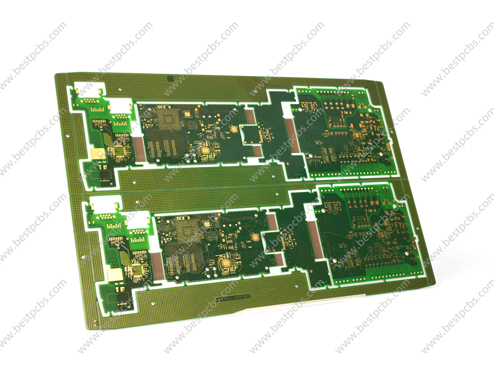
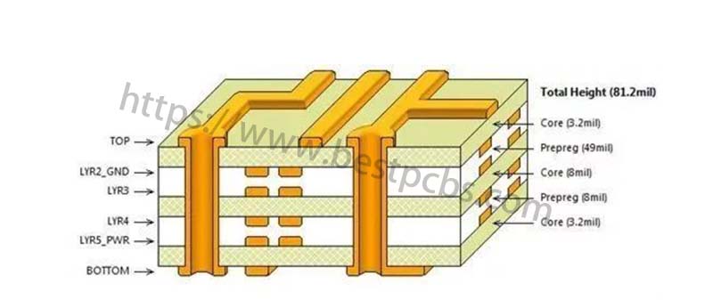
When it comes to multilayer PCB, we know the multilayer PCB are consisted by many different layers. Do you know what’s the purpose for these layers?

Here I would like to give you a brief introduction for the functions of each layer on a Multilayer PCB design.

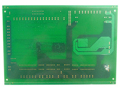
Mechanical layer: There may be one or several mechanical layers in a PCB depending on the design. There should be at least one mechanical layer as it shows the physical dimensions of the board. Generally, it used GM1, GM2 to name the file on the Gerber.

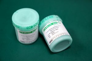
Solder paste layer: This is a material applied onto the PCB layers where components are mounted, mostly through soldering. It helps with the bonding of the solder with the component pin and improves the solder flow. PCB Assembly supplier will make stencil according to the solder paste layer on the Gerber.

Generally, it used GPS, GBS to name the file on the Gerber.

Solder mask layer: This layer is a mask or a protective coating applied onto the board to prevent damage and contamination. It is typically green in color; however, you can also choose other colors such as blue, black, white depending upon your requirements. Generally, it used GBS, GTS to name the file on the Gerber.

Ground planes and power planes: These are layers for copper, the ground and the power planes are connected to an onboard voltage point. Generally, it used GND, PWR to name the file on the Gerber.

Split planes: This is a modified version of power and ground planes; they are split in a manner that they can be connected to multiple voltage points or potentials.

Keep out layer: This layer is crucial as it defines the working boundary and keeps it separate from the outer mechanical layer. Generally, it used GKO to name the file on the Gerber.

Silkscreen layer: This is typically the text displayed on the boards through which you can identify components with their names. It is typically white in color when solder mask color is green, black, blue and red. But you can also choose other colors such depending upon your requirements. Generally it used GTO, GBO to name the file on the Gerber.

Routing layer: These layers help to interconnect the components. They can also be present on the top and bottom layers of the board.

Drilling Layer: This is the layer to show the drilling information of the PCB. Usually, it names DRL on the Gerber.

Once we understand the purpose of each layer for PCB, then understanding the construction of PCB becomes easy, no matter how complicated the board structure.

With over 15 years of PCB manufacturing experience, BEST Technology can meet different requests from customers no matter it is prototype or high-volume PCB.

Send us your request, let us to make the high-quality printed circuit boards for you.

You may also like

Notes for cleaning PCBA

Monday, October 18th, 2021

PCBA includes components assembly and DIP plug-in, in the whole process, there will be reflow soldering, wave soldering, manual soldering, due to the current Electronic products are getting smaller and smaller, and the size requirements of PCBA are getting smaller and smaller, but the requirements for quality (including product reliability and stability, etc.) are getting higher and higher. Many customers require PCBA boards with conformal coating to increase stability and reliability and ensure product quality and performance. But the PCBA board must be cleaned before with conformal coating.

Because there will be a variety of flux residues on the soldered MCPCB board, some of which are acidic, soluble and corrosive, etc., if these residues are not cleaned, the coating will also cause very great damage to the product. In this blog I’d like to share some notes for cleaning PCBA.

  1. PCBA board after soldering, should be cleaned as soon as possible (flux residue will produce corrosion over time), cleaning residual flux and other pollutants on PCBA board.
Copper Core PCB
  • When cleaning the PCBA board, prevent the cleaning agent from intruding into the unsealed components to avoid damage to the components. After cleaning, it should be placed in the oven at about 30-50 degrees, baked for about half an hour, and then removed after drying PCBA board.
FR4 PCB
  • When cleaning the PCBA board, protect the components and labels on the board. Otherwise, the mounted and welded PCBA board will be wasted.
Aluminum Core PCB

Cleaning PCBA board affects the life and reliability of electronic products. Some of PCBA boards are not cleaned, which may lead to short circuit and leakage, leading to unqualified products and many failures, increasing the cost of recovery and maintenance, so it is not worth the loss to clean PCBA boards.

Best Technology has our own SMT factory and can help our customers to buy the components at the same time. If you have any new inquiry of PCBA, welcome to send it to me then I can send you the quotation for comparison with your other suppliers.

You may also like

About the “heat” problem in PCB & MCPCB

Monday, October 18th, 2021

For high-power products, the concept of “heat” is often mentioned, which is especially important in high-power products. It not only determines the service life of the product, but also relates to whether the product can work properly.

We will explain the “heat” problem in circuit board design from three aspects: the generation of heat, the impact of heat on the product and the “heat” in the system layout.

1. Heat generation:

Heat generation in a system takes several paths:

1) Power consumption of the component itself

2) Efficiency of power conversion devices

3) High frequency signal conversion heating

4) Power consumption of contact resistance and wire resistance during signal transmission

2. Impact of fever on products

The operating temperature of components is generally below 80 degree, and the operating temperature of commonly used capacitors and resistors is generally controlled below 50 degree. If the temperature of the system is not controlled, the following conditions may occur:

1) The temperature rise will cause the working parameters of components to change, resulting in the unstable working performance of the whole system.

2) Temperature rise will accelerate the aging of components, affecting the accuracy and life of components.

3) Temperature rise will cause circuit board deformation and poor connection of components.

General heat dissipation components arrangement

3. “Hot” considerations in system layout

1) Selection and layout of the chassis: choose materials with good thermal conductivity, such as aluminum alloy

2) Black heat absorbing material is coated inside the shell to enhance the function of radiation heat absorption

3) The shell is closely combined with the components with high calorific value to conduct heat dissipation

4) A large number of heating components should be placed at the edge of the plate to shorten the heat transfer path. Heat-resistant components should be kept away from light sources.

5) In the design process, the appropriate wire width and copper thickness should be selected, and the influence of wiring density on the current-carrying capacity should also be considered. Copper foil should be filled in the gap of the board surface as far as possible for heat conduction. The heat conduction hole can help effectively heat dissipation and reduce local temperature.

In the design of circuit board, how to effectively control the temperature of the system is a problem that must be considered.

You may also like

Ceramic PCB for Sensor Application

Wednesday, October 13th, 2021

Sensor technology will help us achieve environmental goals surrounding cleaner energy and lower carbon, including the electrification of vehicles; serving autonomous vehicles and smart city infrastructure. It is used to collect big data required for management, control and safety; widely used Applied to the medical market, etc.The application for sensor is becoming more and more popular.

With the continuous improvement of sensor input power, the size of the sensor continues to shrink, and the large heat generated by the large power dissipation puts forward newer and higher requirements for packaging materials. The application prospect of the base sensor is broad, which also has more rigid requirements on the performance of the packaging material itself.

Engine oil level Sensor

The advantages of ceramic materials

1. High thermal conductivity, meeting the heat dissipation requirements of the sensor;

2. Good heat resistance, meeting the application requirements of sensors at high temperature (Higher than 200°C);

3. The thermal expansion coefficient is matched to match the thermal expansion coefficient of the chip material for sensor to reduce the thermal stress of the package;

4. The dielectric constant is small, the high frequency characteristic is good, reduce the signal transmission time of the sensor, improve the signal transmission rate;

5. High mechanical strength, meeting the mechanical performance requirements of sensor during device packaging and application;

6. Good corrosion resistance, able to withstand the erosion of strong acids, strong alkalis, boiling water, organic solutions for sensor, etc.;

7. The structure is compact and meets the requirements of hermetic packaging for sensor.

Fluid level sensor

Some data show that for every 2°C increase in the temperature of electronic components, the reliability decreases by 10%. Obviously, the overheating of electronic components is one of the culprits of the shortened equipment life. To do a good job in thermal management of equipment, ceramic copper clad laminates are indispensable. Best ceramic copper clad laminates have high thermal conductivity (thermal conductivity 180 W/(mK) ~ 260 W/(mK)), which can dissipate heat in time. Ensure the stable operation of equipment and effectively extend the life cycle of sensor or other product.

If you want to know more about ceramic PCB for sensor, please feel free to contact us.

You may also like