X-Ray Inspection’s Definition
X-ray inspection is a technology used to inspect the hidden features of the target objects or products. As for PCB inspection, X-ray is commonly used in the inspection of PCB assembly in order to test the quality and find the hidden defects, X-ray inspection is one of the most important steps for quality-oriented PCB manufacturers.
X-Ray Inspection’s Working Principle
Generally, there are three elements in the X-ray devices.
- X-ray tube—to generate the X-ray photons.
- Operation platform—to move along with the sample so that the sample can be inspected from different angles and magnification.
- Detector—it can capture the X-ray through the samples and then transfer it into the image so that we can find out whether there are defects on the printed circuit board.
The Hidden Defects that can be Identified by X-Ray
Since PCB has the higher density with the solder joints hidden and holes buried or blind, X-ray enable us to inspect the quality of the PCB and identify various hidden defects. And there are three common hidden defects that can be inspected by X-ray.
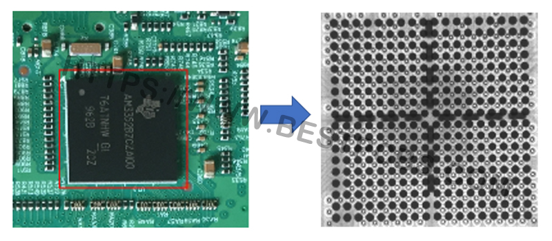
- Solder bridges—it is a common issue that will occur when the solder joints are so close that they create a connection which is not allowed. And usually, the solder bridges will be covered by some components on the PCB. But they can be easily found with the help of the X-ray device.
- Solder voids—when gas or flux is entrained during welding, solder voids will be produced, which will lower the thermal conductivity at the solder joint and may cause physical defects. And X-ray can help to identify the solder voids
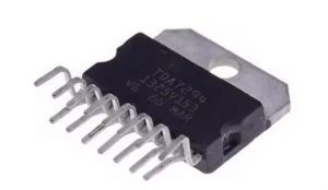
- Pin-hole fills—pin-hole fills issue is a common problem occurring in the plug-in components on the printed circuit boards. The X-ray device can be used to identify these errors, and can even quantify the missing filling amount.
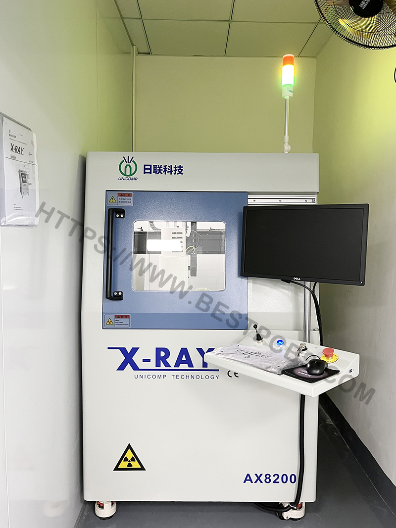
Our X-Ray Inspection Device
The maximum size of the board that can be put in the device’s operation platform is 510*430 mm, while the maximum inspection size of the device is 435*385 mm. So here is the manifestation of the operation platform’s function. When the size of PCB is over 435*385 mm, the operation platform will move along with the board so that the board can be inspected thoroughly.
And here is a video about operation of our X-ray inspection device.
So, this is the end of this article. In case if you have any questions, you are welcome to contact us via email at sales@bestpcbs.com. We are fully equipped to handle your PCB manufacturing requirements.