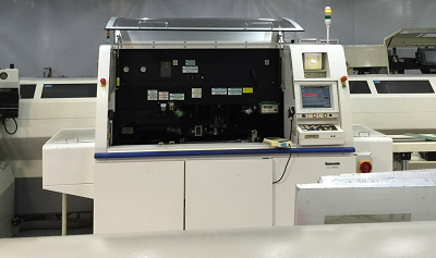
Yes, we produced all kinds of FR4 PCB in one panel and also combine two kinds FR4 PCB together with SMT so far.
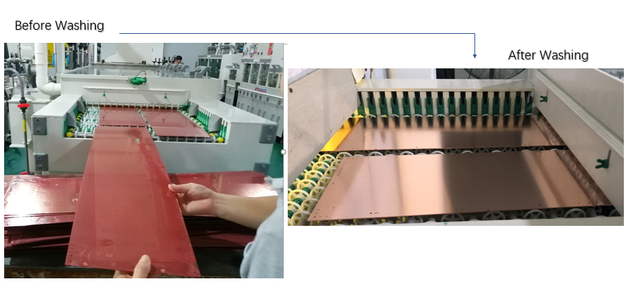
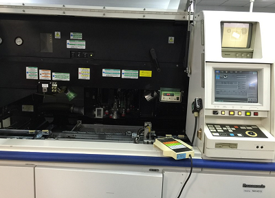
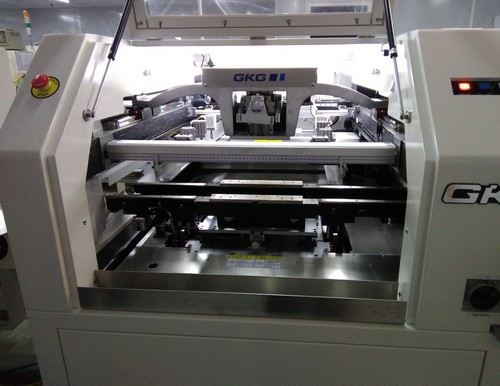
Please check the following pictures to know more detail.
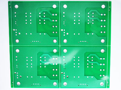
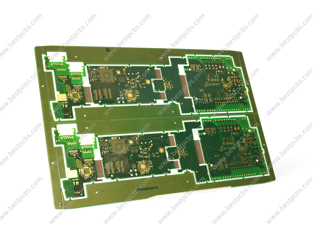
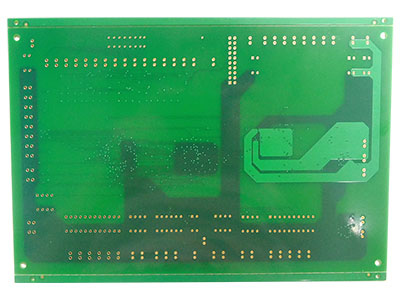
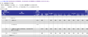
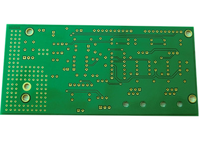
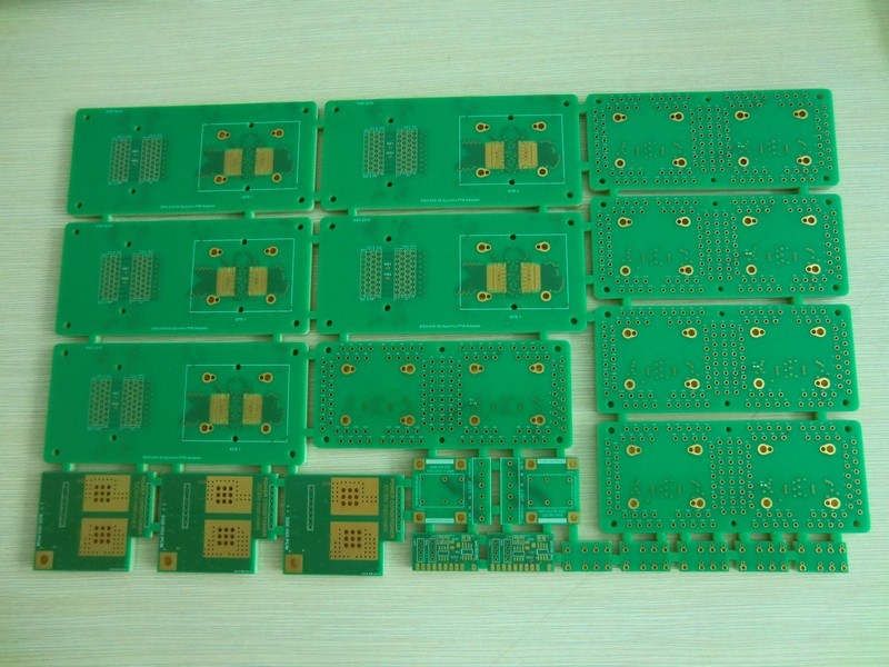
- We put all kinds of boards in one panel to produce, after finish production and separate the boards, you can get several FR4 PCB.
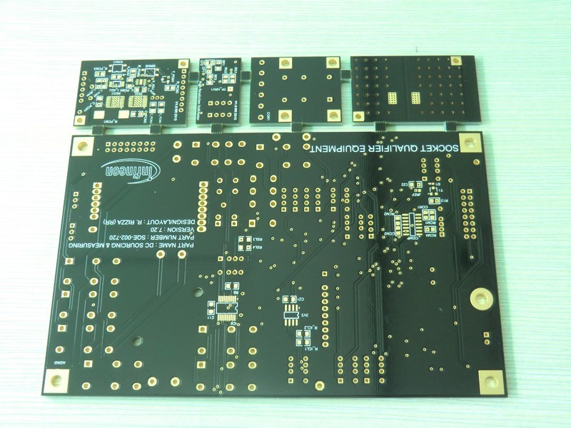
Different design in on panel
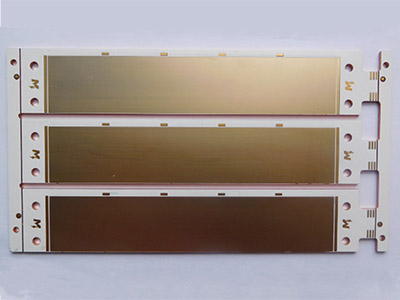
Different design in one panel
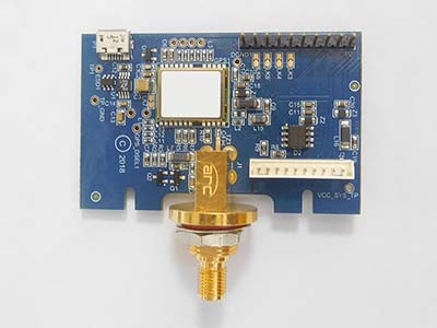
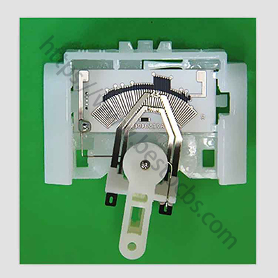
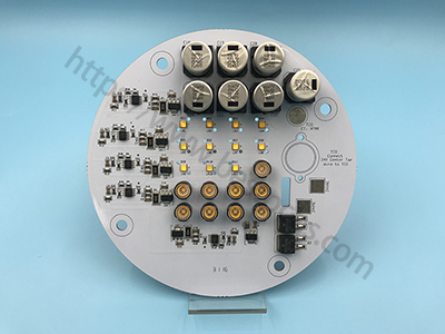
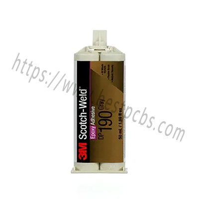
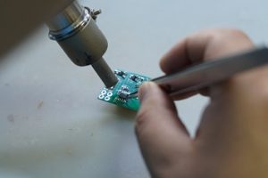
- We produced the bare board separately and combine them with SMT.
We provide turnkey assembly service, so don’t hesitate to contact us if you have any questions about PCB manufacturing and assembly.