Archive for November, 2021

What is RF PCB board?

Tuesday, November 23rd, 2021

You may have ever heard of RF PCB, but do you know What it is and What are the characteristics of these kinds PCB?

Today let us make a simple introduction for it.

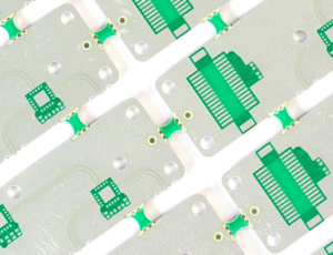
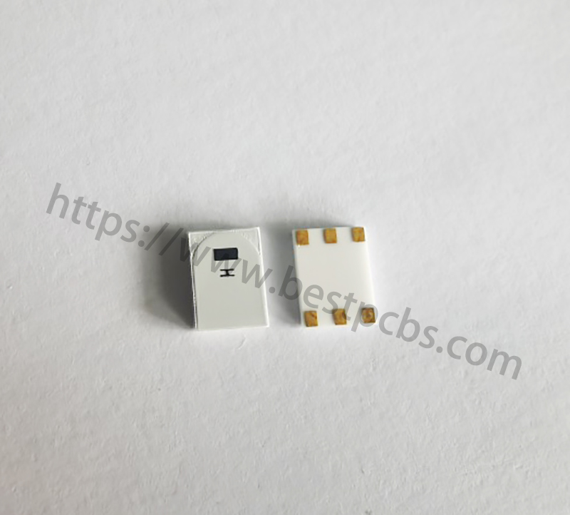
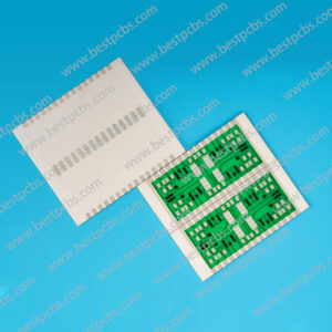
RF PCB, means radio frequency PCB. People also called these PCB High frequency PCB, it is for the PCB with a higher electromagnetic frequency, and it is used on the products field with high frequency. (Frequency greater than 300MHZ or wavelength less than 1 meter) and microwave (frequency greater than 3GHZ or wavelength less than 0.1 meter). It is made by microwave substrate with common PCB manufacturing process or with some special way to make.

High-frequency boards have very high requirements for various physical properties, accuracy, and technical parameters, and are often used in communication systems, automobile anti-collision systems, satellite systems, radio systems and other fields.

How can we know which PCB materials are suitable for making the RF boards?

When evaluating the high-frequency characteristics of a substrate material, the key to its investigation is the change in its DF value (Dissipation Factor).

For substrate materials with high-speed and high-frequency characteristics, in terms of changing characteristics at high frequencies, there are two distinct types of general substrate materials: one is that with the change of frequency, its (DF) value changes very little. There is another type that is similar to the general substrate material in the range of change, but its own (DF) value is lower.

The common epoxy resin-glass fiber cloth-based materials (FR4), the DK value at the frequency of 1MHz is 4.7 and the change of the DK value at the frequency of 1GHz is 4.19. Above 1GHz, the change trend of its DK value is gentle. The change trend is that as the frequency increases, it becomes smaller (but the change is not large). For example, at 10GHz, the DK value of FR-4 is generally 4.15. The substrate material with high-speed and high-frequency characteristics changes in frequency. When the DK value changes slightly, the DK value keeps changing in the range of 0.02 when the frequency changes from 1MHz to 1GHz. Its DK value tends to decrease slightly under different frequency conditions from low to high.

On the other hand, the thermal expansion coefficient of the high-frequency circuit board substrate and the copper foil must be the same. If they are inconsistent, it will cause the copper foil to separate during the cold and hot changes. Secondly, in a humid environment, the water absorption rate must be low, and high water absorption rate will cause dielectric constant and dielectric loss when wet. In general, the heat resistance, chemical resistance, impact resistance, and peel resistance of the high-frequency sheet must be good.

The following are several commonly used high-frequency and high-speed PCB boards we have summarized:

Rogers: RO4003, RO3003, RO4350, RO5880, etc.

TUC: Tuc862, 872SLK, 883, 933, etc.

Panasonic: Megtron4, Megtron6, etc.

Isola: FR408HR, IS620, IS680, etc.

Nelco: N4000-13, N4000-13EPSI, etc.

Other materials like Arlon, Teflon, Taconic are also good for the manufacturing of RF PCB boards.

If you have any question for RF pcb, welcome to send your request and question to discuss more.

You may also like

The SMT production progressing

Thursday, November 18th, 2021

SMT (Surface Mounted Technology) is the most popular Technology and process in electronic assembly industry. SMT refers to a series of process processes based on PCB. Due to the better outcome and higher efficiency, SMT has become the primary approach used in the process of PCB assembly. In some extent, the turn-key service is a way to reduce the cost.

There are the SMT progressing in the following.

1. Solder paste printing: The function is to print the solder paste to the PCB pad to prepare for the welding of components. The screen-printing machine is located at the front end of SMT production line.

(Automatic solder paste printer)

2. Part mounting: The function is to accurately install surface assembly components into fixed positions on the PCB. The equipment is the SMT machine, located behind the screen-printing machine in the SMT production line.

3. Furnace curing: its function is to melt the patch adhesive, so that the surface assembly components and PCB board firmly stick together. The equipment used is the curing furnace, located behind the SMT machine in the SMT line.

4. Reflow welding: The function is to melt the solder paste, so that the surface assembly components and PCB board firmly stick together. The reflow furnace is located behind the SMT machine in the SMT line.

(Reflow soldering)

5. AOI optical detection: its function is to detect the welding quality and assembly quality of assembled PCB board. The equipment used is automatic optical detection (AOI)

(AOI machine)

6. Maintenance: its function is to detect the failure of the PCB board for repair. The tools used are soldering iron, repair workstation and so on. Configured after AOI optical detection.

7.Dividing board: its function is to cut PCBA of multiple connecting boards, so that they are separated to form a single individual, generally using V-cut and machine cutting.

8. Grinding plate: its role is to scrub the burr parts to make them smooth and flat.

9. Washing plate: its function is to remove welding residues such as flux and other harmful to human body on assembled PCB board and manually clean it.

Turnkey service reduces customers’ time in contacting with multiple suppliers for separate steps in PCB assembly manufacturing. And the scientific order arrangement system allows customers to get PCB assembly products with higher quality and less cost in a shorter time than the traditional way of PCB assembly.

(SMT production line)

You may also like

What kind of MCPCB is suitable for your electronic project?

Saturday, November 13th, 2021

If you need a Metal Core PCB for your project, there are some different types can be selected, the selection of the MCPCB type depends upon the type of application and project you are performing. This blog will provide you information about the metal based PCB, which will also illustrate the construction, uses and distinguishing features of the MCPCB boards, hope it can help you to choose the most appropriate MCPCB for your subsequent projects. 

Types of Metal Clad PCB 

There are many different types of the MCPCB depending upon the type of base material, currently the most common metal used for MCPCB manufacturers are Aluminum, Copper and steel alloy. The selection of the base material depends upon the type and nature of the electronic project.

1) Aluminium core PCB

Aluminium is a better material that we can use for the core of a board. The reason is that it has high heat transfer capability. Moreover, it also shows the heat dissipation capacity to the maximum extent. Aluminium is also relavitively cheaper as compared to the copper material. Therefore, it represents the cheaper and better manufacturing of the printed circuit boards.

2) Copper metal core PCB

Copper is the best material for the core of MCPCB, since this material shows the best heat transfer capability. Moreover, this material is also fit for the excellent heat dissipation during the process. These features save the PCBs from the thermal issues.

The copper core PCB shows the best thermal conductivity as compared to other PCBs. The normal value of the thermal conductivity for these PCBs is 2.0W/mk. However, we can get this value of thermal conductivity up to 12W/mk in the case of insulating layer. Therefore, these types of the PCBs have the tremendous use in the high-power LED lights.

3) Stainless steel PCB

Another important material that has an excessive use in the metal core PCBs is the Stainless steel PCB, which also can provide better capability of connectivity and high performance, and it’s more rigid than both aluminum and copper, but thermal conductivity is lower than them too. 

copper core & aluminum core pcb

Stack up of Metal core PCB

The stack up and construction of the MCPCB depends on the number of layers in the PCB. The PCB with the single layer, two layers and multiple layers have the different methods of stack and construction.

1) Single Layer Metal Core PCB

A single layer MCPCB consists of a metal base, Dielectric Layer, Copper Circuit Layer. The advantage is that it provides a better connection between components of the PCB, and it’s efficient at the heat dissipation in the high-power generator systems. These PCBs have the holes on the board for the mounting process of the electronic components. It can also have the screws around the chassis of the board for the arrangement of the components.

Single Layer Metal Core PCB
  • Two (Double) Layers MCPCB / Double Sided More Core PCB

In some cases, there’s not enough space on the single layer PCB for the mounting of enough electronic components. So we need to use the two layers conducting material to resolve this issue.

Regarding the MCPCBs with two layers of copper conductor, there are two basic types, one is Two (Double) layers MCPCB, the other one is Double Sided More Core PCB, which depends on your demand of the mounting of the electronic components, the components can be soldered on both sides on Double Sided More Core PCB.

If you would like to know more details of the differences between Double Sided MCPCB and Double/Two Layers MCPCB, welcome to click following link.

Double Sided More Core PCB

3) Multi Layers metal core PCB

The Multi Layers MCPCB have the more complex and integrated circuit/construction, which can be populated more components on the boards, put signal and ground layer into seperated layers, to achieve better performance in electrical performance. It’s best for heat transferring from electrical components to the chassis of the board. The use of these boards is tremendous in the digital and analogue devices.

Multi Layers metal core PCB

If you have any questions about MCPCB, welcome to contact Best Technology.

You may also like

Ceramic PCB antennas for Bluetooth sports headset

Thursday, November 11th, 2021

What is the function of the built-in ceramic antenna for the s Bluetooth sports headset?

Ceramic antenna is another miniaturized antenna suitable for Bluetooth devices. The types of ceramic antennas are divided into block-shaped ceramic antennas and multilayer ceramic antennas. The block-shaped antenna is to use high temperature to sinter the whole ceramic body at one time, and then print the metal part of the antenna on the surface of the ceramic PCB.

Ceramic PCB for Bluetooth sports headset

The firing of multilayer antennas by low-temperature co-firing. The multilayer ceramic PCB are laminated and aligned and then sintered at high temperature. Therefore, the metal conductor of the antenna can be printed on each ceramic dielectric layer according to the design needed, which can reduce the size of the antenna size and then can achieve the purpose of hiding the antenna. Since the dielectric constant of the ceramic is higher than other PCB, so using ceramic antennas can effectively reduce the size of the antenna, it is very good for Bluetooth sports headset application. 

Ceramic PCB for Bluetooth sports headset

The material of the ceramic antenna is ceramic, and the weight is only 200g. Its frequency range is between 902MHz and 928MHz. In terms of dielectric loss, the ceramic medium has a smaller dielectric loss than the PCB, so it is in the low power consumption rate. The Bluetooth module is very suitable for it. The effect of the ceramic antenna is stronger than that of the on-board antenna. Generally, there are ANT access feet and ground feet, which are also very convenient to use.

Ceramic PCB for Bluetooth sports headset

The principle of ceramic antennas is divided into two parts: one is the transmitting antenna and the other is the receiving antenna.

  • Porcelain antenna transmitting antenna uses an electrode called “antenna” to turn the high-frequency electric field formed between the antenna and the ground into electromagnetic waves, which can be emitted and propagated to a distance.

Ceramic antenna Receiving antenna uses an electrode called an “antenna” to induce electromagnetic waves from the air into an electric field, generate high-frequency signal voltage, and send it to the receiver for signal processing.

Please feel free to contact sales@bestpcbs.com if you want to know more about ceramic PCB

You may also like