pcb
Home > Blog

Archive for 9 月, 2023

What Is The Difference Between Thin Film and Thick Film Ceramic PCBs?
星期一, 25 9 月, 2023

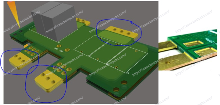
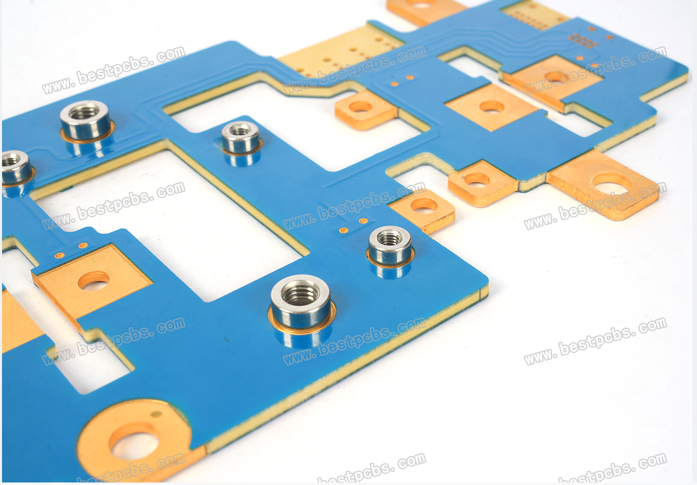
We know due to the rapid development of electronic devices, Ceramic circuit boards have gradually developed into an ideal packaging substrate for a new generation of integrated circuits and power electronic modules. Among them, thick film ceramic substrate and thin film ceramic PCB are the most popular ceramics that be used in package, because they are made by metallization process.

Why use film technology?

Compared with three-dimensional ceramic materials, film has relatively thin thickness and small size, it can be regarded as a two-dimensional structure. Thick film is made by printing process, the thick film can be made independently and the thickness is usually 10~25μm. Thin film is formed by the composition of the conductor materials and it was sputtering on the ceramic substrate directly. Normally the thickness of thin film is equal or less than 1μm. If the metallization thickness between 1μm to 10μm, then we called it as Directly Plated Copper (DPC) ceramic circuit board.

(ceramic_pcb_with_green_glass_glaze)

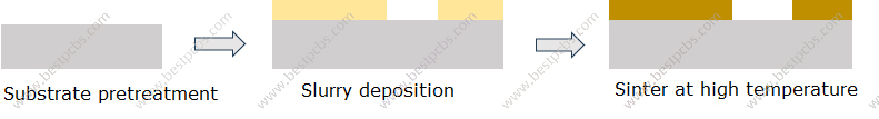
Thick Film Technology

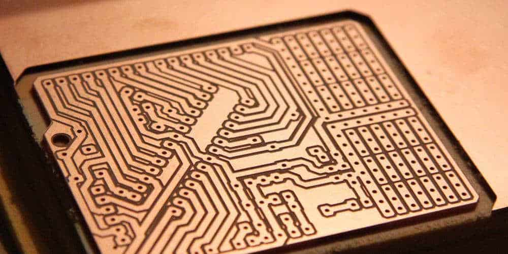
Thick film technology is a method of direct deposition of slurry on substrate through screen printing technology, and sintering at high temperature to form conductive traces and electrodes. After the material is sinter at high temperature, it will form a strong adhesion film on the ceramic circuit board, and after repeated many times, it will form a multi-layer interconnected ceramic circuit board with resistor or capacitor. The thick film manufacturing process is more easier than thin film.

(Simply_process_for_thick_film_ceramic)

Thin Film Technology

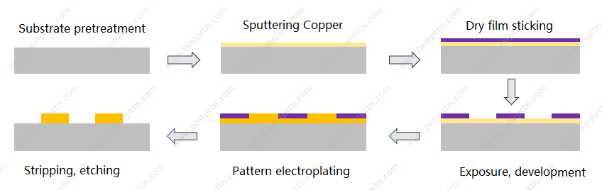
Thin film ceramic PCB is a chip manufacture technology, which is the main method of metal film deposition in microelectronics fabrication. It was made through evaporation and PVD process firstly to deposited a 200-500nm copper layer as the seed layer. Then using electroplating process to increase the copper foil to required thickness. Finally through stripping and etching to generate the circuits. Thin film ceramic circuit is widely used in LED package fields because its fine traces, high accuracy and heat dissipation.

(Manufacturing_process_of_thin_film_ceramic)

Thin film and Thick film ceramic PCB comparison

In addition to the technology manufacturing difference, their performance and limitations also is different. Here we summarized in below table:

TechnologyThick FilmThin Film
Conductor thick10-25um<=1um
Manufacture processScreen printing, sinterPVD, DES
TCR(50-300) *10-6/C(0-50) *10-6/C
CostRelatively LowHigh for prototype
Line widthThicker line widthFine traces, suitable for RF
Bonding abilityNot suitable for bondingGood for wire bonding
ResistanceAvailableNeed mount resistors
Solder maskAvailableAvailable

Application difference between Thin film and Thick film ceramic PCB

The applications of thin film and thick film also are different because of their different features. Thick film ceramics are widely used in high power devices such as automotive field, power electronics, aerospace due to its ability to handle high current and voltage. Thick film enables to provide excellent thermal management and can dissipation heat effectively. Thin film ceramic PCBs trend to micro-electronics and RF devices because of its fine lines, low resistance, and high-frequency performance.

Each technology has its unique advantages and limitations, it needs to be properly used to make it suitable for different electronic devices and industries. Choose the right ceramic PCB substrate for laymen is a big challenge, so seeking for a reliable supplier is important. Best Technology engaging ceramic circuit board manufacturing for over 10 years. And our core engineering team are deep in this industry for more than 20 years, we are so confident that we can provide the best solution for you. If you are interested in this, welcome to contact us at sales@bestpcbs.com.

You may also like

What is Bus Bar PCBs in the Electronics Landscape?
星期五, 22 9 月, 2023

Bus Bar PCBs are a specialized type of printed circuit board (PCB) that stand out from traditional PCBs due to their integrated conductive bus bars. These bus bars are typically made of copper or aluminum and are positioned on the surface or within the PCB. They serve the purpose of connecting electronic components, devices, or connectors and transmitting electrical currents.

Key Characteristics:

Outstanding Heat Dissipation:

Bus Bar PCBs are renowned for their exceptional heat dissipation capabilities. The integrated conductive bus bars efficiently conduct and dissipate the heat generated within the circuit, making them an ideal choice for high-power applications. Whether it’s in industrial electronics, electric vehicles, or solar inverters, this characteristic ensures that electronic components stay cool, enhancing overall system reliability.

Compact Space Utilization:

Space is often a precious resource in electronic devices. Bus Bar PCBs optimize space utilization through their integrated conductive bus bars. Unlike traditional wiring systems that can be space-consuming, Bus Bar PCBs save space, reducing the overall footprint of electronic systems.

Enhanced Electrical Performance:

The integration of conductive bus bars reduces the overall resistance and inductance of the circuit, resulting in improved electrical performance. Lower resistance translates to reduced power loss, while decreased inductance facilitates faster signal propagation. This, in turn, leads to higher efficiency and improved signal integrity.

Conclusion:

Bus Bar PCBs represent a force of innovation in the field of electronics, with their exceptional heat dissipation, space-saving design, and enhanced electrical performance making them highly favored across a multitude of applications. As technology continues to advance, Bus Bar PCBs are expected to play an increasingly pivotal role in the design and manufacturing of electronic systems.

If you have any interest in Bus Bar PCBs or any related requirements, please feel free to contact us. We have been in the field of heavy copper PCB manufacturing and bus bar PCB manufacturing more than 17 years. We are committed to providing you with outstanding products and services. Let’s explore the limitless possibilities of Bus Bar PCBs together, bringing innovation and success to your projects!

You may also like

Do you know the relationship between copper thickness and circuit width & spacing?
星期六, 2 9 月, 2023

We know the precision control and performance of a product are paramount, only know that PCB can be built with a nice function, so, to understand the intricate relationship between copper thickness and circuit width and spacing is pivotal. These two parameters are like the gears of a well-oiled machine, interlocking in ways that significantly influence the printed circuit board‘s functionality, signal integrity, and manufacturability. If the designer does not consider the relationship between these two, the design may need to be modified in subsequent production.

In order to avoiding this information, let’s embark on a deeper exploration of this dynamic relationship to uncover its nuances and implications now,

Frist of all, we need to know some basic information about PCB, like copper thickness, circuit width and spacing.

  1. The Essence of Copper Thickness

Copper, known for its exceptional electrical conductivity, is the lifeblood of any PCB. The copper thickness refers to the amount of copper deposited onto the board’s surface during fabrication. It’s the foundation upon which the traces, the intricate pathways that carry electrical signals, are built. The standard copper thickness is often measured in ounces per square foot (oz/ft²) or micrometers (µm). Common options include 1oz (35µm), 2oz (70µm), and even higher, it depends on customer’s requirement.

  • Circuit Width and Spacing

Circuit width and spacing, though often overlooked, are integral components that determine a PCB’s performance, integrity, and overall functionality. Circuit width refers to the dimension of the conductive traces, while spacing pertains to the distance between these traces. These seemingly simple dimensions have a profound impact on the PCB’s behavior.

Secondly, Unveiling the Intricate Relationship

The relationship between copper thickness, circuit width, and spacing is a sophisticated interplay of electrical properties, heat dissipation, and signal integrity. Let’s delve deeper into this complex web of interactions:

Current-Carrying Capacity and Copper Thickness: Copper thickness directly influences a trace’s ability to carry current without succumbing to overheating. Thicker copper translates to higher current-carrying capacity and reduced resistive losses. However, the trade-off is that wider traces are necessary to accommodate the increased copper thickness.

Resistance and Circuit Width: Wider traces exhibit lower resistance, which in turn reduces voltage drop and enhances the efficiency of signal transmission. Designers must strike a balance between trace width, copper thickness, and available board space.

Spacing and Unwanted Interactions: As circuit spacing decreases, the probability of unwanted interactions, such as crosstalk and electromagnetic interference, rises. Thicker copper can exacerbate these issues due to its larger cross-sectional area. Maintaining appropriate spacing between traces is pivotal to prevent signal degradation and maintain integrity.

Heat Dissipation and Trace Width: Thicker copper also aids in better heat dissipation, a crucial consideration for power-intensive applications. However, this can necessitate wider traces to manage the thermal load effectively.

Signal Integrity and Crosstalk: Smaller spacing reduces the risk of crosstalk, but it’s a double-edged sword. Thicker copper traces may introduce higher capacitance, altering impedance and potentially impacting signal integrity. This delicate balance requires careful consideration during design.

For now, we have known the relationship between them, how to develop a best design between the circuit width & spacing and copper thickness, which depends on what’s you really want, the huge current or heat management? Following details should be considered if you want to develop the best circuit width & spacing.

Current Requirements: Start by understanding the current requirements of your traces based on the components and operational conditions. Selecting the appropriate copper thickness and trace width ensures the PCB can handle the anticipated loads.

Thermal Management: Thicker copper facilitates heat dissipation, which is advantageous for power-dissipating components. However, remember that it might necessitate wider traces to ensure effective heat transfer.

Manufacturability: While thicker copper can enhance current-carrying capacity and heat dissipation, it might pose manufacturing challenges. Consult with PCB manufacturers to align your design choices with their capabilities.

Signal Integrity Analysis: Utilize simulation tools to analyze signal integrity, especially when dealing with smaller spacing and thicker copper. These tools provide insights into impedance matching, potential crosstalk, and overall performance.

Flexibility VS Rigidity: While thicker copper enhances many aspects, it can impact the PCB’s flexibility, crucial for certain applications. Evaluate the mechanical demands of your project and strike the right balance.

Regarding metal core PCB in Best Technology, the copper thickness and its accordingly circuit width & spacing like below, furthermore, it would be better if you can let me know your copper thickness before checking your drawing, we will give you the best solution before formal production.

Copper thicknessMinimum circuit widthMinimum circuit spacing
0.5-2oz0.25mm0.23mm
3oz0.35mm0.3mm
4oz0.4mm0.38mm
(trace_design_guide_of_MCPCB)

Conclusion: Striking the Optimal Balance

The intricate relationship between copper thickness, circuit width, and spacing in PCB design embodies a delicate equilibrium that significantly influences a design’s performance and functionality. This nuanced interplay directly impacts parameters such as current-carrying capacity, resistance, heat dissipation, and signal integrity.

Achieving the optimal balance between these factors requires a deep understanding of electrical properties, thermal considerations, and signal behavior. Designers must carefully evaluate the specific requirements of their projects and leverage simulation tools to fine-tune their choices. Collaboration with PCB manufacturers ensures alignment with manufacturing capabilities.

The dynamic nature of this relationship underscores the constant evolution of PCB technology. As devices become smaller, faster, and more interconnected, the demand for intricate layouts intensifies. Designers must continuously adapt to new challenges, pushing the boundaries of what’s achievable while adhering to the fundamental principles that govern PCB design.

You may also like

Why do ceramic substrates contribute to the breakthrough of 905nm lidar technology?
星期五, 1 9 月, 2023

LiDAR (Light Detection And Ranging, referred to as “LiDAR”) measurement is a system that integrates three technologies: laser, GPS (Global Positioning System), and IMU (Inertial Measurement Unit, inertial measurement unit), used to obtain data and Generate accurate DEMs (Digital Elevation Models). The combination of these three technologies can highly accurately locate the spot of the laser beam on the object, and the ranging accuracy can reach the centimeter level. The biggest advantage of lidar is accurate, fast, and efficient operation.

Lidar is currently widely used in the field of driverless cars and robots. It is known as the “eye” of a generalized robot. It is an active measurement device that measures the precise distance between an object and a sensor by emitting laser light.

  As an indispensable sensor for L3 and above automatic driving, lidar has significantly improved the reliability of the automatic driving system with its excellent ranging capability, high angular resolution and sensitivity to ambient light, and has become the key to improving reliability. A key element of autonomous driving systems, but its application is constrained by cost and technical challenges.

  In the past, lidar was difficult to apply to mass-produced vehicles due to its high cost. However, recently, with the continuous evolution of technology and market competition, the cost of lidar has gradually decreased, thereby accelerating its application in the field of autonomous driving.

In this evolution process, the emergence of ceramic substrates has played a vital role in the breakthrough of lidar technology – 905nm wavelength lidar has become mainstream. Traditional materials such as FR-4 and FE-3 are difficult to meet the high heat dissipation requirements of lidar, while ceramic substrates rely on their excellent thermal conductivity. For example, the thermal conductivity of aluminum nitride ceramic substrates is as high as 200W/M.K. It effectively solves the heat dissipation problem and provides a guarantee for the stability and life of the lidar.

In lidar, the transmitter is one of the links with the highest value and the highest barriers. On the transmitter side, with the rise of China’s domestic industrial chain and the adjustment of the overall technical route of the industry, among them, 905nm VCSEL laser chips and other products have achieved breakthroughs in the market and become a hot topic in the industry.

The “heart” of the transmitter is the light source. Laser transmitter is the core component of laser technology, and its composition includes laser working medium, excitation source and resonant cavity. In this system, why choose a ceramic substrate as a component? The main reason lies in its unique advantages in heat dissipation. Especially for VCSEL (Vertical Cavity Surface Emitting Laser) chips, due to their low power conversion efficiency, the problem of heat dissipation is particularly prominent. The application of ceramic substrates has become the best choice to solve the problem of thermoelectric separation.

The ceramic substrate has excellent heat dissipation performance and can effectively conduct the heat generated inside the laser transmitter. The high thermal conductivity of the ceramic substrate allows it to efficiently conduct heat generated inside the lidar, preventing performance degradation due to overheating. In addition, ceramic materials have the advantages of high strength, hardness, thermal shock resistance, insulation, and chemical stability, which can further extend the service life of products, improve sensitivity, and enhance the response speed of lidar.

Ceramic substrates also enable high-density assembly, supporting miniaturization and integration of devices. Its stability ensures that the sensor signal is not distorted, and the matching with the thermal expansion coefficient of the chip ensures the reliability of the product in harsh environments such as high temperature, high vibration, and corrosion. In addition, the metal crystallization performance of the ceramic substrate is excellent, which ensures the stability of the circuit and further improves the quality control level of the lidar.

As a leading manufacturer of ceramic substrates, Best Technology provides a variety of ceramic substrates of different materials, including 96% alumina, 99% alumina, aluminum nitride, zirconia, silicon nitride, sapphire ceramic bases, etc. The heat dissipation properties of these different materials are different, such as aluminum nitride (AlN): thermal conductivity of 170-230 W/mK, silicon nitride (Si3N4): thermal conductivity of 20-80 W/mK, sapphire (Al2O3): thermal conductivity Coefficient 25-40W/mK.

Therefore, choosing a high-quality ceramic substrate not only helps to solve the problem of thermal and electrical separation of laser emitters, but also provides stable heat dissipation and electrical performance, providing reliable support for efficient operation and performance improvement of laser emitters. In the development of lidar technology, ceramic substrates play an increasingly important role, providing key support for performance breakthroughs and innovations in laser transmitters. We are witnessing a revolution in the auto industry brought about by China’s autonomous driving assistance systems.

If you are designing a ceramic PCB and seeking a reliable manufacturer, welcome to leave you message or contact us directly.

You may also like