pcb
Home > Blog

Archive for 2 月, 2023

“TEN Q & A” about Ceramic Printed Circuit Board
星期一, 27 2 月, 2023

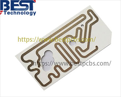
Q1: What do the abbreviations DBC and AMB stand for?

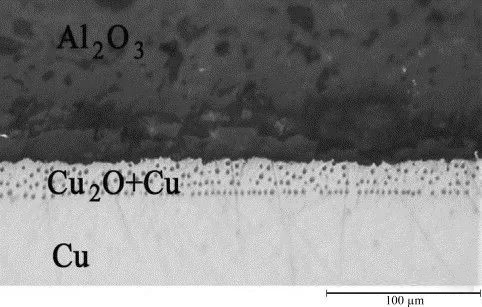
A: DBC means “Direct Bond Copper” while full name of AMB is “Active Metal Brazed”. Both abbreviations refer to bonding technology of attaching a relatively thick copper (generally more than 0.2mm) on the ceramic substrates. These two technologies can be used to fabricate metalized ceramic substrates.

Q2: What is the mainly difference between DBC and AMB?

A: The mainly difference is AMB need to braze the copper to a ceramic board by active metal while DBC can directly connect the copper and substrate without any additional materials.

Q3: Which kind of ceramics are suitable for DBC and AMB?

A: DBC technology is suitable for oxide ceramics such as Al2O3 and ZTA. Non-oxide ceramics must be oxidized before they can be bonded to copper by DBC technology. ALN can be made into DBC or AMB ceramics, but Si3N4 only can be used as AMB substrates.

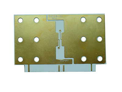
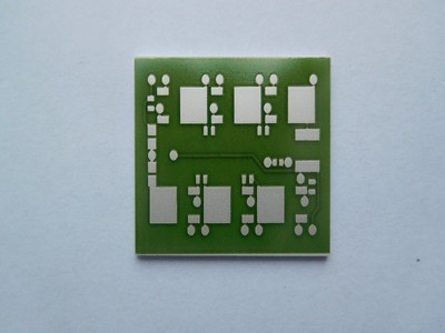
Q4: What is the function of metalized ceramic PCB?

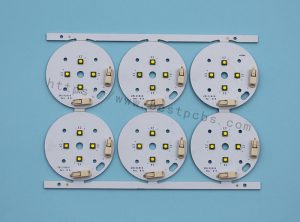
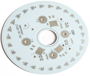
The metallized ceramic substrate needs to carrier and interconnect multiple power semiconductor devices. The resulting electronic components are called power modules or multi-chip packages, most commonly LED packages or semiconductor packages. 

Q5: Does AMB can be used with oxide ceramics?

A: Yes, but the effective of DBC technology is better and the cost is relatively lower.

Q6: What is the most important performance need to be considered when design a new ceramic PCB?

A: It depends on the end application of product will be used in. Ceramics are chemically inert substances that are resistant to corrosion, moisture, and high temperatures, making them preferable to organic dielectrics that degrade in corrosive environments. Electrical, thermal and mechanical properties are equally important in the design of a new substrate. Dielectric strength is an important factor to meet the isolation requirements, which should be set according to the standards, specifications and regulations of the target application. Low thermal conductivity is not conducive to the heat transfer between the chip and the surrounding environment. The bending strength and fracture toughness play an important role in prolonging the service life of the substrate under thermal-mechanical stress.

Q7: How to choose a suitable substrate?

A: First, the heat dissipation of power semiconductor devices should be understood. Then, based on the chip and the ambient temperature, the required substrate thermal resistance is calculated. However, the combination of copper and ceramic may not always achieve the desired thermal resistance.  For one thing, the isolation voltage determines the minimum thickness of the ceramic. On the other hand, the thickness ratio of copper to ceramic has a great effect on the reliability. Finally, the set of applicable standards will be very limited.

Q8: Are DBC and AMB substrates suitable for high voltage applications?

A: The DBC substrate is ideal for applications with operating voltages up to 1.7 kV.  For higher operating voltages, a thicker ceramic layer is required to meet the relevant isolation requirements.  Silicon nitride (ALN) is often used because its high thermal conductivity offsets the increased thickness. In addition, resistance to partial discharge is particularly important in this application. Thus, AMB is superior to DBC techniques for this purpose unless the interfacial gap between copper and ceramics can be eliminated.

Q9: Are DBC and AMB substrates copper plated only on both sides?

A: No, both of two technologies can plate copper only on one side. But this is not a standard combination of materials, however, because the resulting flatness of the substrate is critical in multiple applications.

Q10: What are the shapes of substrates?

A: The rectangle is the cheapest and most common shape to produce. Other shapes are also available, but may incur additional production costs.

You may also like

The Difference Between 2L MCPCB and Double Sided MCPCB
星期一, 27 2 月, 2023

In our last article, we know what a metal core PCB is, in this post, we will introduce what is the difference between 2L MCPCB and Double sided MCPCB. Please continue to read if you want to know more about metal core printed circuit board.

Today we will explain from these four contents as following:

  1. Stack up (structure)
  2. Heat dissipation
  3. SMD populate
  4. Manufacturing technology

Stack up of 2L MCPCB and Double Sided MCPCB

For a 2L MCPCB, the metal core is positioning on the bottom side of the MCPCB as a cooling carrier to the whole MCPCB, while the metal base of double sided MCPCB is located in the middle of two copper trace. In generally, some PTH (plated-through-hole) vias are needed to designed to connect the bottom and top traces.

Below are the stack ups of these two kinds of products, from the structure, we can easily distinguish which one is 2L MCPCB and which one is double sided MCPCB.

Heat dissipation of 2L MCPCB and Double Sided MCPCB

Due to the different structure of the two products, their heat dissipation performance is also different. The main reason is the heating of double-sided metal core circuits can be spread out through both top and bottom side, while the heating generate by SMD components of 2 layers circuit only can be dissipated through bottom (metal) side and the heat need to go down layer by layer. In addition to this, the dissipation of FR4 is not good than metal materials, so double-sided metal core printed circuits perform better heat dissipation performance than 2 layers MCPCB.

Surface mounted locations (SMD populate)

Nowadays, surface mounted technology (SMT) is widely used in printed circuit board industry, more and more designers prefer to populate electronic components of the circuit surface to achieve high density, stable electrical performance and high reliability. 2L metal core circuit boards and double-sided metal core circuits also show their different mounted locations in this aspect.

The populate location of a 2L MCPCB only available on copper trace side, that is top side. And a double-sided metal core PCB can mount components on both top and bottom side, because both of them exist copper trace on it.

Manufacturing technology

May somebody will curious about “Are these two products produced in the same process/technology?”

The answer is obvious “NO, they have a different laminate process when fabricating.”

Different with single layer MCPCB, double sided MCPCB requires an additional pressing step to laminate the thermal conductive layer and metal core together. But sometimes, some raw Metal Clad material vendor will supply board material which already laminated.

For 2 layers metal core PCB, due to it is made of a single MCPCB and a double-sided FR4 PCB, the first thing we should make a double sided FR4 PCB, then laminate the PCB together with the single MCPCB. But due to the thermal conductive layer (pure adhesive) is easy to overflow during laminating process, which will cause the poor adhesion and crack between metal core and FR4 PCB. In the meantime, to avoid such problem, an experienced operator is needed to proceed the laminated process. That is why the lead time and cost of a 2 layers metal core circuit is much longer and expensive.

This is the end of this post, if you still have some questions or difficulties about the metal core PCB, welcome to contact us at sales@bestpcbs.com, our professional sales team and engineering team will give you a best solution for free.

You may also like

Do You Know What a Metal Core PCB Is?
星期六, 25 2 月, 2023

Metal Core Printed Circuit Board (short for MCPCB) is a technology developed to overcome the thermal limitations of the FR4 Printed Circuit Board. Different with traditional FR4 PCB, the PCB uses FR4 material as base core, while the base material of a metal core PCB is aluminum or copper. So compared with FR4 PCB, Metal Core is a better choice if your boards need to perform in high temperature environment.

What is metal core PCB?

A Metal Core PCB (MCPCB), also known as a thermal PCB or metal backed PCB, is a type of PCB that a metal material as its base for the heating dissipation part of the board. The thick metal is covering one side or double side of the PCB. The purpose of the core of a MCPCB is to redirect heat away from critical board components (such as LED or IC chips), and to less crucial areas such as the metal heatsink backing or metallic core. Base metals in the MCPCB are used as an alternative material to FR4 boards.

(Metal_core_PCB)

Same as FR4 PCB, the metal core PCB can be divided into Single layer MCPCB, Double layers MCPCB and Multi-layer MCPCB.

  • Single layer MCPCB

A single layer MCPCB is consist of a metal base (usually aluminum or copper alloy), thermal conductivity/dielectric layer and a copper trace layer, you can check below stack up for more details. Due to it only has one layer copper trace, sometimes we called it as one-layer MCPCB or single sided MCPCB.

(Stack_up_of_single_layer_MCPCB)

The single sided MCPCB can be used with surface mount and chip & wire components, and provides much lower thermal resistance than FR4 PCB. What’s more, the metal core provides lower cost than ceramic substrates, and allows much larger areas than ceramic substrates.

Meanwhile, superior heat dissipation and good durability of Aluminum of metal core PCB can greatly eliminate heat sinks or other some voluminous hardware for engineers or designers.

  • Double layer MCPCB

Double layers MCPCB (2L MCPCB) has two copper layers on one side of PCB, and metal core as a base core on the bottom side of whole MCPCB, so the components only can be populated on the top side, below is a structure of double layer MCPCB.

(Stack_up_of_double_layers_metal_core_PCB)

From the stack up of double layers MCPCB, we can see it consists of a single layer MCPCB and a double sided FR4 PCB, so it needs an additional pressing process to laminate the thermal conductivity and FR4 PCB. Compared with normal FR4, this structure needs more technology and experience on laminating of two layers together with metal core.

There are two layers copper trace on the surface of MCPCB, can we call it as double sided MCPCB like single layer MCPCB?

The answer is NO, because they have different structure and perform different properties. In our next post, we will show you the differences between double sided MCPCB and 2 layers MCPCB.

  • Multi-layer MCPCB

Same as FR4 PCB, for those copper traces more than 2 layers, we named them Multi-layer MCPCB. Its structure is same as FR4 PCB, but more complex to fabricate. Below is a typical stack up of a 4 layers MCPCB:

(Stack_up_of_4L_MCPCB)

Contrast with single layer or double layers MCPCB, multi-layer MCPCB can populate more components and achieve better performance in electronical performance.

Why Choose Metal core PCB?

Metal core PCB offers a great list of advantages when apply in a high-power application, below we listing some benefits of it:

  • Excellent heat dissipation
  • Lower thermal expansion than FR4 PCB
  • Dimensional stability than polyimide FPC
  • Great durability
  • Long lifetime
  • High utilization rate of space due to the heating can be transferred quickly
  • High strength and lightweight than FR4 PCB
  • Cost-effective

Where can we use Metal core PCB?

Metal core PCB can be used in high-power filed where requires fast cooling, good heat dissipation characteristics, the following popular applications may give you a guideline:

  • LED lighting
  • Power suppliers
  • Power conversion system
  • Automotive electronics
  • Telecom industrial
  • Photovoltaics
  • Semiconductors

With more than 16 years manufacturing experience, Best Technology is one of MCPCB supply leaders in Asia with good metal core PCB capability, we are so confident that we can provide you high quality, fast delivery and excellent one-stop service. Warm welcome to contact us if you have inquiries.

You may also like

What is the DBC Ceramic Copper Oxidation Technology
星期一, 20 2 月, 2023

DBC (Direct Bond Copper) ceramic PCB also known as DCB ceramic, which is widely used in various type of high-power semiconductor, especially in IGBT package material by means of its excellent electricity and thermal conductivity of copper and the advantages of high mechanical strength and low dielectric loss of ceramics. DBC technology uses the oxygen-containing eutectic solution of copper to directly apply it to the ceramic. The key factor in the preparation process is the introduction of oxygen element, so the copper foil needs to be pre-oxidized in advance. Do you want to know what is the copper foil oxidation technology during the DBC ceramics manufacturing? Hereinbelow, we will introduce the oxidation process for you.

Oxidation technology of copper foil

Copper oxidation is divided into Wet Air Oxidation (including soaking oxidation and spraying oxidation) and Dry Oxidation.  Both oxidation methods can form CuO or Cu2O on the surface of copper foil.

  • Wet Air Oxidation (WAO)

i. Soaking oxidation

First, the copper is pickled with 3% dilute sulfuric acid, and then washed by the spray washing machine after overflow. Next, sent the copper into the mixed solution of potassium permanganate and copper sulfate (the concentration of potassium permanganate is about 31.6mg/L and the copper sulfate is about 95.4mg/L) for soaking and oxidation.  The oxidized copper is then washed with water and three-stage countercurrent washing, and then slowly pulled for dehydration and drying (the temperature is about 100℃) to complete soaking and oxidation.

ii. Spraying oxidation

Spraying oxidation is a kind of WAO, only the oxidation method become spraying. Spray oxidation is to spray copper with mixed solution of manganese nitrate and copper nitrate (concentration of about 3%) after pickling and washing.  The sprayed copper is dried directly in the tunnel kiln (the temperature is about 200℃).  In the drying process of tunnel kiln, the manganese nitrate and copper nitrate sprayed on the copper sheet are decomposed into copper oxide and manganese oxide.  The ratio of soaking oxidation and spraying oxidation treatment of copper sheet is about 5:5.

  • Dry Oxidation

Dry oxidation is very easy to process, put the copper into oxidation oven firstly, then heating up to 600~800oC for oxidizing around 30mins and then subjected to air cooling annealing.

Wet Air Oxidation VS Dry Oxidation

At present, the existing industry is widely used to finish the high-temperature annealing oxidation of copper then sintering with ceramic substrate, that is dry oxidation.  But this high temperature annealing, oxidation in one way has some drawbacks as following:

  1. Uneven oxidation. It will directly cause sintering defects during sintering, and the peeling strength will change greatly.
  2. Leaving conveyor belt marks.  Because the high temperature and oxidation process is transported by the conveyor belt, the existence of the conveyor belt mesh will affect the temperature distribution of the entire copper is not uniform, leaving marks/traces of the conveyor belt.  The result of sintering is to leave the corresponding trace on the bonding surface of CuAl2O3.
  3. High temperature annealing and oxidation will accompany the grain growth of copper. In the subsequent sintering process, the grain will continue to grow, which brings adverse effects on the mechanical properties and surface treatment of copper.  The copper surface grain produced by wet oxidation is fine, which is conducive to improving the mechanical properties of copper and eliminating the traces of conveyor belt. The main difference between wet oxidation and dry oxidation is shown in the bending resistance, heat resistance cycle performance and peeling strength, and these three indicators are significantly better than dry oxidation. Wet oxidation products can better meet the requirements of bending strength and heat resistance cycle performance.

So, this is the end of this post, Best Technology specialized in fabricating ceramic PCB (including DBC, DPC, AMB, HTCC and LTCC technology) for more than 16 years, we have rich engineering team and professional sales team can provide one-stop service for you. Welcome to contact us if you have any inquiries about ceramic PCB.

You may also like