Recently customer compliant that the soldermask for some holes, esp for PTH (plated through hole, sometimes people named Via) was wrong, because in his original Gerber file, it was opened, but on actual printed circuit board, it was tented (covered), and some cases, some was tented and some was opened at the same time. It made customer confused.
In fact, there’s a default rule in PCB (printed circuit board) manufacturing: If the PTH (Via) was less than 0.60mm, then the soldermask will be made as per factory’s default rules: making them as tented (covered), regardless it was tented or opened in customers’ original Gerber file.
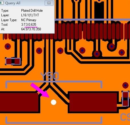
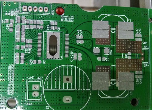
Here you can see pictures showing a board with a 0.30mm PTH, soldermask was opened in original Gerber file, but in real board, it was tented.
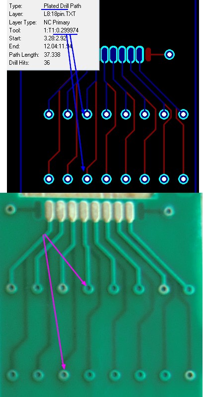
0.3mm Via soldermask
And in this board, for 0.508mm PTH (via), some soldermask was opened and some was opened.
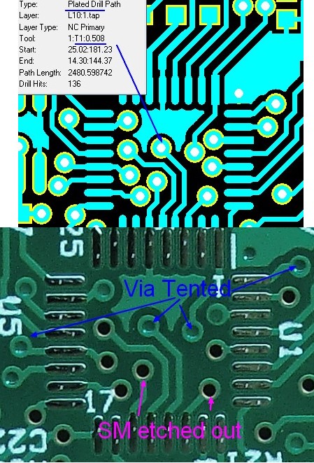
0.508mm Via soldermask
Why like that? Here are two major reasons:
1) For PTH(via) less than 0.6mm, normally the function was only to electrically connected trace, not for electronic components assembled; so whatever PTH was opened or tented, it doesn’t matter.
2) In rigid printed circuit board manufacturing, it’s not easy to etch away the soldermask around PTH less than 0.60mm. As soldermask was made by that method: printed whole area with oil (soldermask), then undergo develop & exposure, then pass the etching line. The chemical will etch away the oil accordingly to the drawing, but if the hole was too small (less than 0.60mm), then the oil around will be very difficult to etch away, so you will see some oil was etched away (soldermask opened), some oil still here (soldermask tented)
If diameter of hole was bigger than 0.60mm, then it’ll be easy to etch away and some of them will be used in assembly, so we will make according to Gerber file and you will see the board exactly like the drawing. See bellowing a picture showing a board with 0.889mm (0.035mil) PTH.
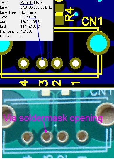
0.889mm Via soldermask opening
Sometimes, people just use these hole as testing point, not for assembly, then we suggest to add another PAD connected to this hole so that you can test it easy. To tested on hole was not stable as tested on a PAD.
In a conclusion, in future, if the hole was less than 0.60mm and you really want it to be opened, please add special notes when release order, and allow us to enlarge the opening diameter of soldermask (around 0.60mm) so that soldermask of these holes will be opened.
Please contact us if still any question about soldermask opening.