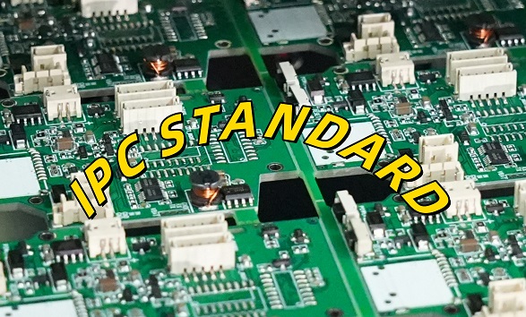
Do you know what is IPC standard for PCB?IPC, it is a trade association whose goal is to standardize the assembly and production requirements of electronic devices and components. It was established in 1957 as the Institute of Printed Circuits. IPC has developed thousands of standards and specifications to regulate the electronics manufacturing industry.
IPC standards are related to PCB design, production technology, electronic assembly, etc., in order to achieve high reliability, high quality, high performance, and meet user specifications.
What are the IPC Standards for?
Before we can understand IPC standards, we first need to know who made them. It comes from the IPC Association, a trade association whose goal is to standardize assembly and production requirements for electronic devices and components. It was founded in 1957 as the Printed Circuit Research Institute. Its name was later changed to the Institute for Electronic Circuit Interconnection and Packaging to highlight the expansion from bare boards to packages and electronic components. In 1999, the organization officially changed its name to IPC with the slogan “Association Connecting Electronics Industries”.
IPC standards are the most widely recognized code of acceptability in the electronics industry. The organization publishes standards for nearly every stage of the electronic product development cycle, including design, procurement, assembly, packaging, and more. In other words, IPC standards refer to everything in the electronics industry and are the basic knowledge of designers and manufacturers.
Just like the IPC standards tree, there are many different aspects of standards that all serve the end product. IPC-A-610, for example, focuses on the acceptability of electronic components and is used worldwide by original equipment manufacturers and EMS companies.
What is the PCB IPC Standard?
IPC plays a vital role in the PCB industry by establishing standards that cover every stage of PCB production from design to manufacturing. These standards ensure consistency and compatibility throughout the PCB process. During the design phase, IPC standards guide file formats, PCB design software, design guidelines, and electronic product documentation. They also affect the material selection of PCB components, surface mount equipment and surface treatments. In addition, these standards are essential for testing and evaluating the acceptability of printed boards.
When it comes to welding, IPC standards cover a variety of techniques, including reflow soldering, wave soldering and welding. These guidelines help companies determine whether their electrical and electronic components meet quality expectations during manufacturing. IPC standards also address cable and harness assemblies to ensure they meet standards.
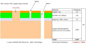
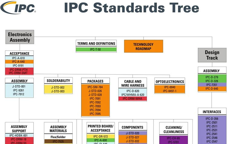
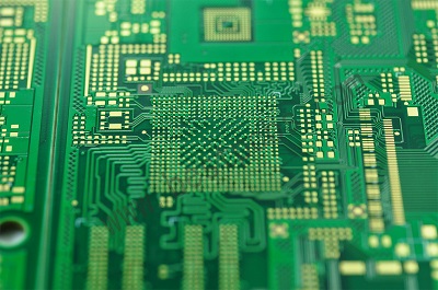
The most widely recognized IPC standard for PCBs is IPC-6011, which Outlines the performance requirements for PCBS. However, IPC-6012 is more specific and governs the qualification and performance of rigid PCBs. IPC-6012 covers everything from how the PCB should be made to its thickness and the integrity of the copper layer. Compliance with this standard ensures that PCBs meet electrical and mechanical performance expectations. Whether you’re creating boards for high-end computers or small consumer devices, compliance with PCB IPC standards is critical to meeting industry and customer expectations. Here is the IPC tree for your reference:
What is the IPC Level of PCB?
One of the most widely used industry standards in the manufacturing of printed circuit boards is IPC-A-610C Acceptability of Electronic Assemblies and IPC-A-600 Acceptability of Printed Boards. This standard is used primarily for the incoming inspection of bare boards from a PCB fabricator.
In the IPC-A-610C document, electronic products are divided into level 1, level 2, and level 3. The higher the level, the stricter the quality inspection conditions. Here are how 3 levels divided:
Level 1 products: called general-purpose electronic products. Including consumer electronic products, certain computers and their peripherals, and products whose main purpose is to use functions.
Level 2 products: called dedicated service electronic products. Including communication equipment, complex industrial and commercial equipment and high-performance, long-life measuring instruments. Under normal use environment, this kind of product should not malfunction.
Level 3 products: called high-performance electronic products. Including high-reliability, long-life military and civilian equipment that can continue to operate. This kind of product must not allow any interruption failure during use, and at the same time, it is necessary to ensure the reliable startup and operation of the equipment in a harsh environment. Such as medical life-saving equipment and all military equipment systems.
For PCB manufacturing, do you know which IPC standards are commonly used?
IPC Standard for PCBs
The IPC has created several standards for printed circuit board (PCB) design, manufacturing, and assembly. Here I would like to share you some standards which we mainly use:
- IPC-2221
A general standard that covers almost every aspect of PCB design, including electrical considerations, thermal design, and manufacturing-ready design.
- IPC-2222
A guide for rigid PCB cross-sectional design, including recommendations for board thickness, hole aspect ratio, and dielectric clearance.
- IPC-2223
A standard for reliable Flex-PCB design, including guidelines for material selection, impedance control, and pad placement.
- IPC-2224
A standard for PC card form PCBs, including design requirements for organic and inorganic materials, and single, double, or multilayered interconnections.
- IPC-A-610
A standard for PCB assembly that classifies PCBs into three quality levels, with Class 1 being the lowest and Class 3 being the highest.
- IPC-6011
General Performance Specification for Printed Boards
- IPC-6012
Appraisal performance and specifications for Rigid printed boards
- IPC-6013
Appraisal performance and specifications for Flexible printed boards
- IPC-6016
Fixed performance and specification of HDI or printed circuit board of high density interconnection layer
- IPC-SM-840
Appraisal and performance of permanent performance
- IPC-HM-860
Multilayer Hybrid Circuit Specification
- J-STD-003
Solderable test for printed boards
- IPC-A-600F
Acceptance conditions for printed boards
- IPC-4761
Design Guide for Protection of Printed Board Via Structure
What is IPC-A-610 Standard?
IPC-A-610 Standard is one of the most widely recognized standards in the electronics industry, specifically focusing on the acceptability of electronic assemblies. It provides detailed guidelines and criteria for the inspection of PCB assemblies, so that these assemblies meet the necessary quality levels for their intended use. Its main content includes:
1. Soldering Criteria
IPC-A-610 provides in-depth guidelines on acceptable soldering techniques, covering solder joints, surface mount devices (SMDs), through-hole components, and wire terminations. It explains what constitutes an acceptable versus defective solder joint, ensuring that the electrical connections are reliable.
2. Component Placement
The standard includes criteria for the correct placement and alignment of electronic components on PCBs. It specifies the acceptable tolerances for misalignment and ensures components are correctly placed for proper electrical performance and physical integrity.
3. PCB Assembly Defects
IPC-A-610 details different types of assembly defects, such as insufficient solder, tombstoning, lifted pads, and more. Each defect is categorized based on its severity and impact on the function and reliability of the product, providing guidance on whether a defect can be accepted or if it requires rework.
4. Classes of Electronic Assemblies
The standard divides electronic assemblies into three classes based on the end-use of the product:
- Class 1 – General electronic products
- Class 2 – Dedicated service electronic products
- Class 3 – High-performance products
5. Mechanical Assembly
IPC-A-610 provides criteria for the mechanical aspects of PCB assemblies, such as mounting hardware, screws, connectors, and wire routing.
6. Coating and Potting
The standard covers the application of protective coatings (conformal coatings) and potting materials that protect the PCB from environmental damage such as moisture, dust, or chemicals. It specifies acceptable thicknesses, coverage areas, and inspection methods.
7. Cleaning Requirements
The cleanliness of PCB assemblies is critical for preventing performance degradation over time. IPC-A-610 outlines acceptable levels of residues from fluxes and other contaminants and specifies methods for inspecting and verifying cleanliness.
8. Cable and Wire Harness Assemblies
The standard includes requirements for assembling and inspecting cable and wire harnesses.
9. Solderless Wire Wraps
The standard also touches on solderless wire-wrapped connections, which are used in some applications where soldering is not practical or preferred. IPC-A-610 defines the acceptable criteria for such connections.
10. Inspection and Testing
The IPC-A-610 standard provides guidelines for visual inspection and testing methods used to evaluate whether an assembly meets the required acceptability criteria. This can include both automated and manual inspection processes, depending on the class of product.
Why IPC Standard is Important?
IPC standards are of great importance to the circuit board industry.
1. IPC standard specifies the requirements for all aspects of the design, manufacturing and assembly of the circuit board, including material selection, size specifications, welding quality, reliability testing, etc., providing a unified reference and guide for circuit board manufacturers to improve product quality and reliability.
2. IPC standards can help communicate and cooperate between PCB manufacturers and customers. By referring to IPC standards, the two parties can reach a consensus on PCB specifications, quality requirements and other aspects, reduce misunderstandings and disputes, and improve production efficiency.
3. For customers, IPC standards provide confidence. When a company adheres to these standards, they can trust that the final product will be reliable and durable, even in demanding environments.
4. In addition, IPC standards also contribute to the technological innovation and development of the circuit board manufacturing industry. By being in line with international standards and understanding the latest technological trends and standard requirements, manufacturers can continuously improve production processes and equipment, improve production efficiency and product quality, and enhance competitiveness.
At the same time, IPC regularly updates and revises standards to meet changing technology and market needs.
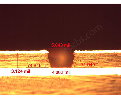
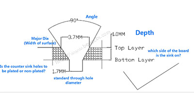
What is the IPC Standard for PCB Clearance?
PCB clearance, or the distance between conductive components, is essential to avoid electrical shorts or interference. Without proper clearance, electrical shorts could occur, potentially leading to device failure or safety hazards. The IPC-2221 standard covers PCB design and provides guidelines for this clearance, ensuring safety and functionality. This standard specifies how much space is needed between traces, pads, and other conductive materials depending on the operating voltage. However, the minimum clearance between any two conductors on a PCB depends on the device’s intended use and voltage:
- General-purpose devices: 0.1 mm (4 mils)
- Power conversion devices: 0.13 mm (5.1 mils)
- Class 2 and 3 PCBs: 0.25 mm (10 mils) for low voltage and 0.5 mm (20 mils) for high voltage
What are the IPC Standards for PCB Repair?
PCB repair can be tricky, but IPC-7711/7721 offers guidance on how to properly rework and repair PCBs. These standards provide detailed procedures for everything from removing defective components to repairing damaged traces and soldering issues.
By following IPC-7711/7721, technicians can restore a PCB to its original condition without compromising its performance. This is critical in industries where PCBs are expensive or difficult to replace, such as aerospace and medical devices. Repair standards also reduce the environmental impact by extending the life of the PCB, making repairs more sustainable.
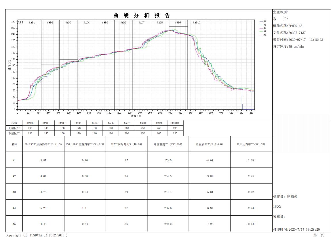
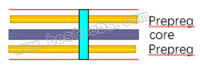
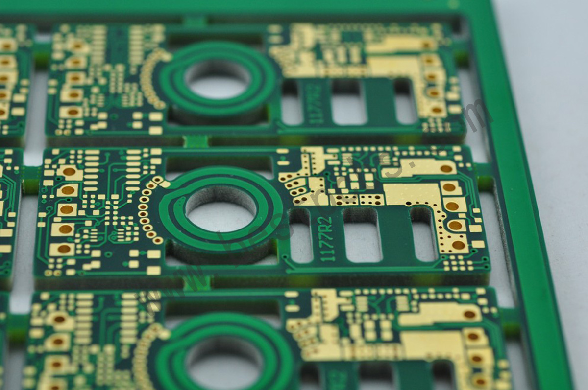
It is no problem for us to manufacture the PCB following the standard in IPC 6012 /6013 Class 2 and Class 3, as well as following to the standard listed above. These acceptance conditions are the basis for the inspection of our company’s products, as well as the working standards of the employees at the production site, and also become an important part of the training of the employees for PCB production and assembly in our company.
Send us your PCB drawing, let’s help to make your PCB design into a real board.