Archive for September, 2020

What’s the Countersink and counter bore on a PCB drawing?

Wednesday, September 30th, 2020

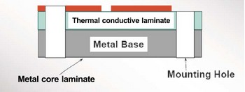
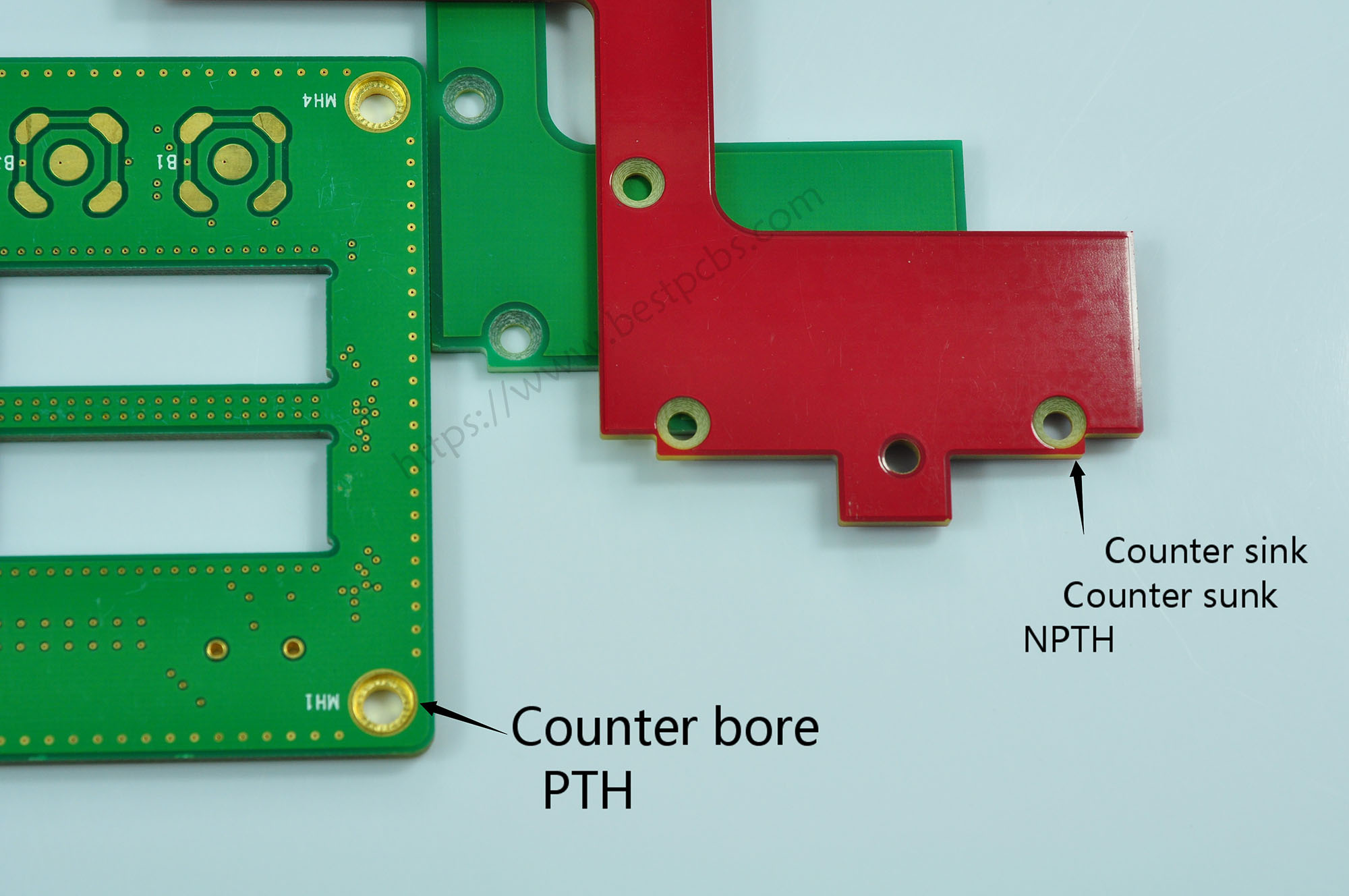
Firstly, do you know what’s a countersink and counter bore?

By definition, a countersink is a stepped hole, which can allow the fasten parts head to sink fully to the parts.

With counter sink on your design, the tapered head of a screw can sit flush with the top of the laminate, commonly countersink is used to install bolts or other connecting parts.

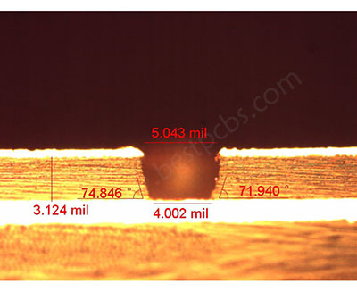
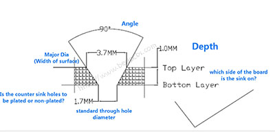
Below is the example for the hole drawing and picture for a countersink:

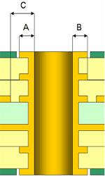
Picture: counterbore holes attributes

To drill your countersunk holes accurately in our PCB fabrication plant, the following information is need to be defined when you supply the PCB drawing for us to make the PCB:

  • Which side of the board is the countersink hole should be drilled, on top or bottom?
  • Is the sink and shaft to be through plated or non-plated?
  • Taper angle or countersink angle. 82°, 90°,120° etc.
  • Countersink diameter of top
  • Countersink diameter of bottom (body)
  • Depth of the countersink is to be drilled(the height of the screw to determine the countersink depth.

By comparison, a counterbore makes a flat-bottomed hole and its sides are drilled straight down. This is usually used when a fastener such as a bolt or cap head screw is required to sit flush with or below the level of a surface.

Below is the drawing and picture for a countersink.

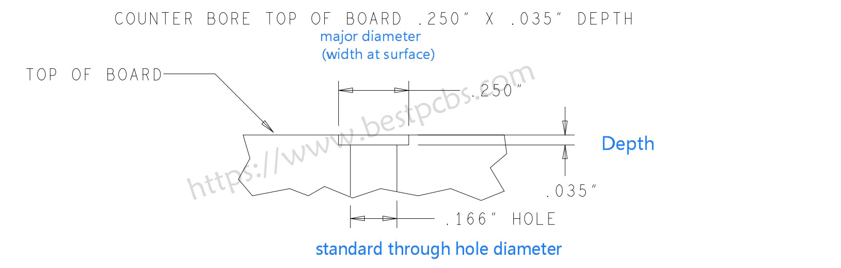
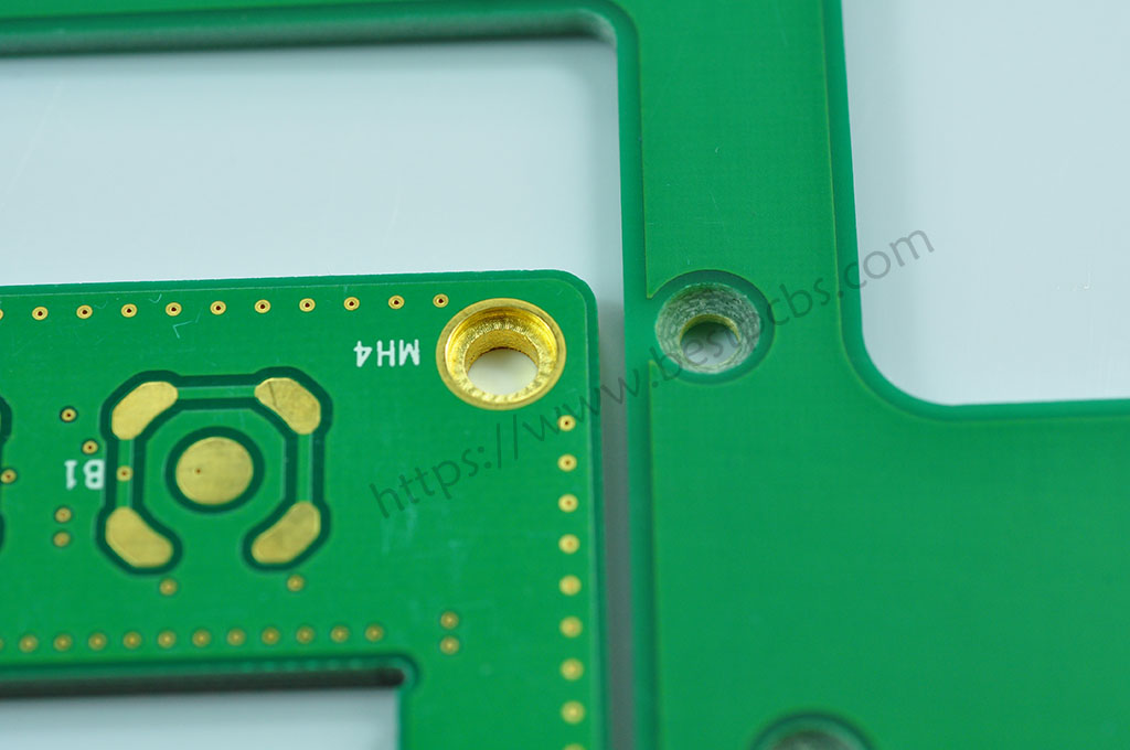
Same as the countersink, the counterbore holes attributes drawing is needed to supply with your PCB drawing when fabricate the counterbored holes. But for counterbore on PCB, because the sides of the hole are always parallel, there is no need to specify the angle.

With below drawing, believe it will be more helpful for you to understand the difference for a counter sink hole and counterbore on the printed circuits board.

If need to have any question regarding the counter sunk or counter board on a PCB drawing, please contact us feel free.

You may also like

What are the factors affecting cost of the MCPCB?

Tuesday, September 29th, 2020

Best Technology considers all the factors affecting the cost of MCPCB production while formulating final cost structure. Many customers contact us to know the factors which affecting the price. The factors are Size & Thickness, Number of layers, Cu Thickness, Thermal Conductivity, Surface Finishing etc.

Size & Thickness: Since larger boards require more material.

As you know, 1.6mm is the standard thickness, if you choose non-standar thickness (Thicker or thinner than 1.6mm), sometimes the price will need to increase, it depend on the layers of your MCPCB.

The different number of layers and manufacturer technology:It’s the main factor for affecting the manufacturing price, therefore the circuit board designing is done in such a manner that it comprises a minimum number of circuit layers. 

Thermal Conductivityis one of the most important performances of MCPCB, the higher the thermal conductivity is, the more expensive the price is. At present, the highest thermal conductivity we can provide is 8W/m.K, the commonly used thermal conductivity is 1-3W/m.K

Cu Thickness: The cost will be more expensive if the copper is thicker. We can provide 0.5 OZ, 1.0 OZ, 2.0 OZ, 3.0 OZ, up to 10 OZ.

Surface Finishing: The common Surface Finishing for MCPCB is HASL_LF, OSP  ENIG (The normal thickness of gold is 1u’’). ENIG is more expensive since the gold is expensive and it with good performance for protecting the surface from oxidized.

ENIEPIG is good for wire bonding (the normal thickness of gold is 3u”).

We always strive to formulate a competitive price structure for our customers, this enables to have a considerable reduction in the total prices and deliver superior quality services to them. If you would like to know more about MCPCB, please directly contact our sales Tammy

You may also like

What is an HDI FR4 PCB?

Wednesday, September 16th, 2020

HDI abbreviation means High Density Interconnect. HDI PCBs have extremely density trace spaces and lines, micro vias under 0.25mm(10mil), smaller pads and higher connection pad density. See the photo of HDI board laser drill& prepreg thickness ratio.

It is very helpful in enhancing electrical performance and HDI PCB use for high-end products and HDI PCB is regularly used in 4G network communications, medical, Military and Aerospace. See the HDI board which Best Tech made for customers.

HDI PCB is the better option for high-layer count and costly laminated boards. Due to the increasing complexity of design structures laminate, the Blind vias and Buried vias are increasingly used in high-density circuit boards (HDI PCB board). Best Tech always improved manufacture capability for HDI, following production capability of the comparison for 2020 and the capability which Best Tech want to achieve at year 2021.

Following is the advantages to use an HDI PCB

The common reason for using HDI technology is a significant increase in packaging density. In addition, overall space requirements are reduced will result in smaller board sizes and fewer layers. 

1.Denser trace

2.More stable performance

3.Reduce interference inductance and capacitance effects

4.Improve signal integrity in high-speed design

5. Reduce frequent relocation of components

What’s mean for a blind via hole?

It is a hole runs from an outer layer, but not through the entire PCB. These holes can be drilled mechanically or using laser technology.

And what’s mean for a buried via hole?

This is a hole that runs between one or more inner layers. They are normally mechanically drilled.

By the way, we would like to make some explain for the through via hole, see attached photo to know the detail.

Do you want to know the different types for HDI PCB boards?

The following photos mainly shows the different laminate structures available from Best Tech for HDI PCB for prototype and mass production.

What is the minimum pad size of hole on the outer and inner layer?

This is different from manufacturer to manufacturer, but in general you can say that the majority of manufacturers can produce them as follows:
A = 0.10 mm
B = 0.15 mm
C = 0.20 mm

Finally, here is an 8L HDI FR4 PCB which we made for our customer at June. See the stack up information.

Surface finish: ENIG(2u”)

Features

1. 3+(2)+3  HDI FR4 PCB board

2. L1 L2、L2 L3、 L3 L4、 L5 L6、 L6 L7、 L7 L8 laser blind hole, micro via size:0.15mm

3. L3、L6 mechanical blind hole, hole size:0.25mm, through hole:0.3mm

4. minimum trace width and space is 3/3mil

5. Finished board thickness: 1.3±10%

6. following is the stack up information

For more information for HDI PCB, welcome to send any query to Best Tech for advice.

You may also like

Why don’t use BeO as substrate to make DBC ceramic PCB?

Wednesday, September 9th, 2020

It is widely known that BeO with high thermal conductivity (200-250W/m.k).

High dielectric constant 6-7 (0.1MHz) and dielectric loss tangent is 10-4 (0.1GHz).

It is ideal material for ceramic PCB, lots of engineers want to use it as DBC ceramic PCB substrate.

But it is unfeasible, the powder of BeO is extremely poisonous.

The poison gas is produced by the reaction between oxygen, Cu and BeO under

1065-1085 degrees Celsius, so it is limited to make cooper on BeO substrate,

it has caused AlN (Aluminium Nitride) is becoming more and more popular.

Though BeO is unfeasible for DBC technology, but it is feasible for thick film technology.

Because when doing the conductor (Au or AgPd) on BeO substrate, we use silk-screen printing, no need to under high temperature environment, there is no chemical reactions.

Below the manufacturing process for your reference.

Here is the photo of BeO with AgPd conductor.

You may also like

If only the LED pad can be made as SinkPAD?

Friday, September 4th, 2020

According to our earlier blogs about SinkPAD introduction,

we can know that the high power LED’s thermal pad can touch the convexity area of copper core directly, so the heat of LED will be dissipated into the air much faster and more efficient than conventional MCPCB, but if only the LED pad can be designed as SinkPAD?

This image has an empty alt attribute; its file name is Stack-up-s.jpg

Actually the pads of other chips or components also can be designed as SinkPAD, one of the most common is the IC pad. In some designs, IC needs to pass through the large current, so it will emit a lot of heat.

This image has an empty alt attribute; its file name is Contrast-images-s.jpg

In order to dissipate heat in time, some customers will directly design the IC solder pad as sinkpad to directly contact the copper base, so that the life cycle will be longer.

As you can see the following picture, it’s the copper layer after doing Etching, the area with blue film we normally named it as convexity, the thermal pad of IC will touch the convexity directly to achieve the purpose of dissipating the heat very fast.

This image has an empty alt attribute; its file name is Convexity-s.jpg

If you have other questions about SinkPAD, welcome to contact Tammy (Email:sales9@bestpcbs.com), she will prove you professional suggestions and solutions.

In the end, I’d like to share the manufacturing process of SinkPAD Board with you, please Click here: SinkPAD-Board-Manufacturing-Process-Best-Technology.pdf

You may also like