Archive for April, 2023

5 PCB Testing details to make your PCB no more quality issues

Monday, April 24th, 2023

As we all know, it is very important to get a well-functional PCB from the PCB manufacturers.  A well functional PCB means that the electricity testing has been performed well at the PCB manufacturer end. However, you may have found some PCB you purchased are with some electricity issues like short & open circuits, or some visual issues like solder pad missing., etc.

Do you know how this issue come while the PCB testing process?

According to the feedback come from the customers, here we summarized some improper ways during the PCB Electricity testing process which may lead to the PCB fail to the test.

Here are some major points for your reference:

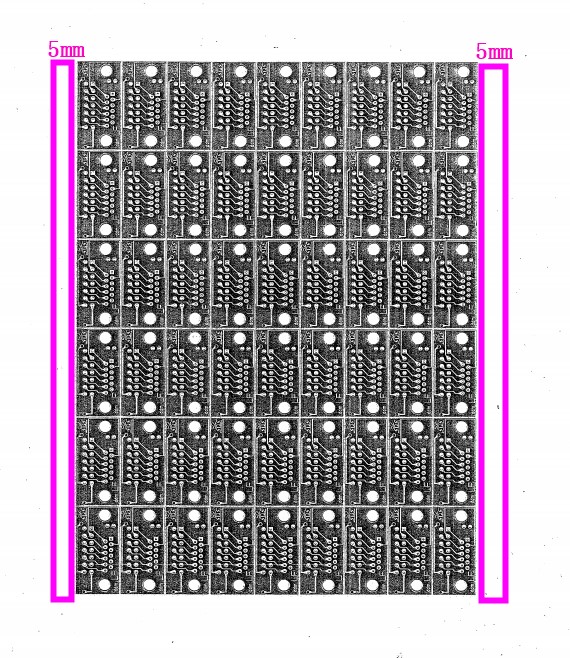
  • Incorrect direction when placing PCB board on testing worktop, the force on probes will cause indentation on boards.
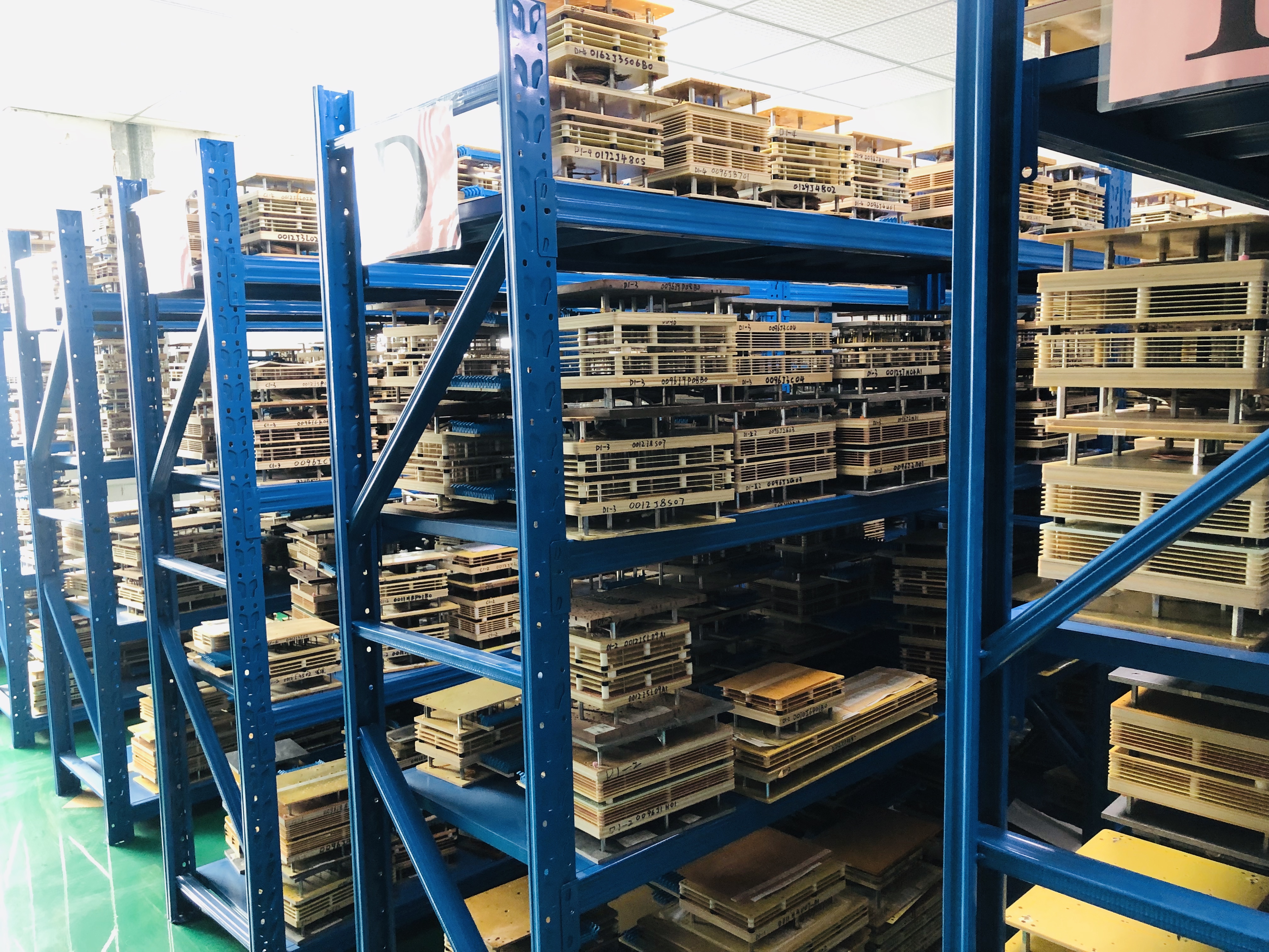
  • PCB manufacturers don’t regularly maintain their testing jig, causing some malfunctions on testing jig can’t be found in time. Take the counter for example, if we do not find the counter’s fixing screw loose in time, it will cause the counter to fail to read the caliper scale. Of course, it also could be the counter is dysfunctional sometimes.
  • PCB manufacturers don’t regularly check/change the testing probes. Dirt on the testing probe cause testing results is inaccurate.
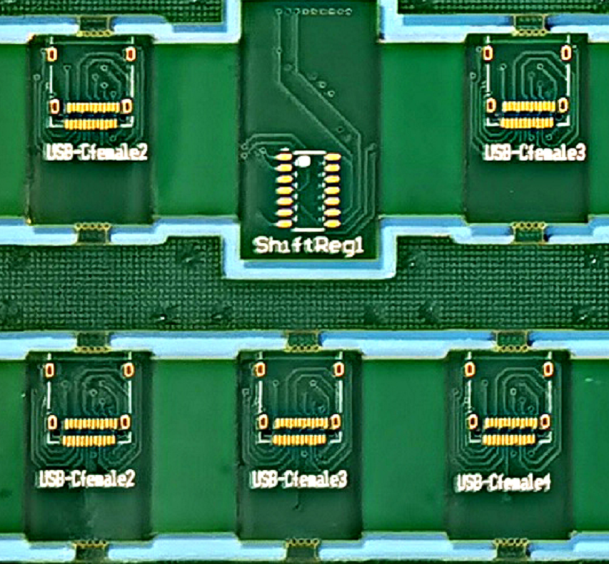
  • PCB testing operator don’t distinguish functional board from NG board due to unclear placement area.

So, if the circuit boards testing work under above improper way, do you know what effects will be on your products?

Base on some lessons learned from our customers, you may get following influences caused by improper way of the PCB testing.

Increase your quality issues

The low testing accuracy will make the functional PCB mixing together with the defective PCB.  If the PCB testing defects can’t be found in time before PCB assembly, defective products will flow into the market, which will seriously increase the quality risk hidden on the end products.

Delay your Progress

After defective PCBs are found, repairing will greatly delay the progress of the project.

Increase your overall cost

The defective PCB will cost many people and time to check and follow, this will directly to increase the overall cost of the projects.

We know deeply that poor testing will bring serious consequences for customers, so with more than 16 years experiences on Printed Circuits Board fabrication, Best Technology has rich experiences on PCB electric testing managements, and following are some of our management solutions to control our PCB testing process:

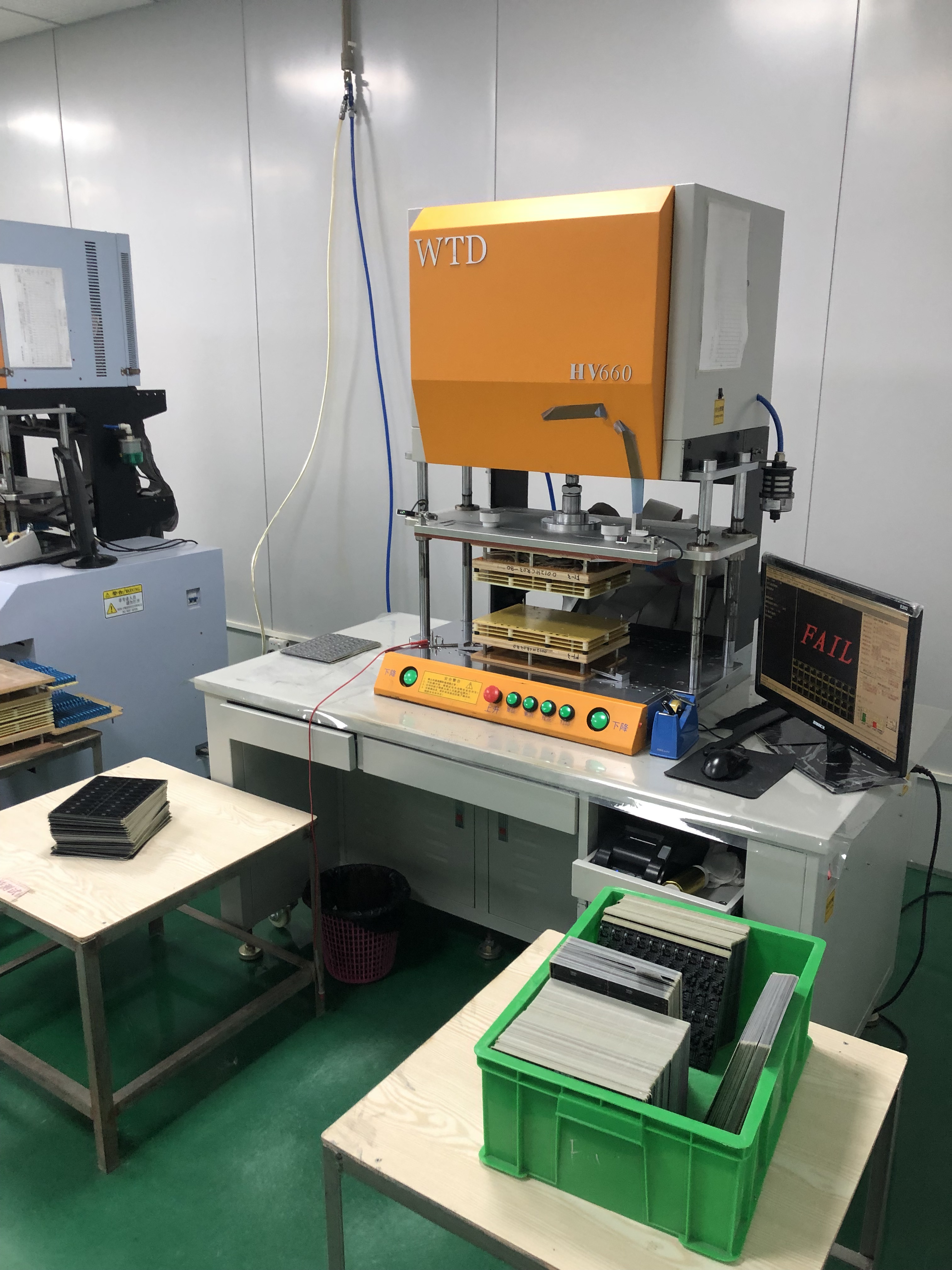
1.   We execute strictly the pre-job training 3 months in advance for the testing operator, and all the testing will be operated by the professional and experienced testers.

2. Maintain or replace the test equipment every 3 months, and use a brush to clean the tester in a regular period or replace the pin cable head to make sure there is no contaminate at the test probe.

3. Add the extra tooling hole at rails for fix purpose to make sure the placement of PCB orientation is no mistake during testing process.

4. The testing workshop must be divided clearly for the qualified board and NG board, the location to keep NG board will be marked with red line.

5. The testing process must be strictly followed with our internal PCB testing standard operating procedure.

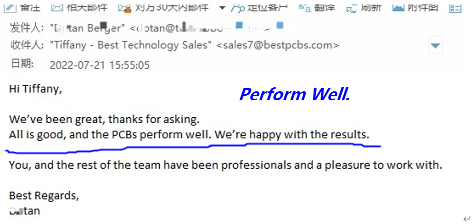
With the help from above management solutions for the PCB E-Testing during the PCB manufacturing process, the PCB we send to customers works very well, which also make sure their products can be assembled well and deliver well in the markets. For us, more and more kindly feedback regarding the functional feedback comes from our customers, here are some good feedback from customers for your reference.

If you have any questions about PCB testing or PCB manufacturing, please feel your freely to leave your message or contact us. In our next update, we will share which test methods are used in the during the PCB Assembly.

You may also like

Can I Design Via Holes in Thick Film Ceramic Boards?

Tuesday, April 18th, 2023

May some engineers or designers who be interested in thick film ceramic circuit are curious about can thick film ceramic boards design with via holes like FR4 PCB? Herein, we will explore the feasibility of using thick film ceramic boards for via holes, including the materials and processes involved, as well as the advantages of this approach.

What is thick film ceramic board?

The “Thick Film” refers to the thickness of conductor layer on a Ceramic PCB. Normally the thickness will be at least 10um, around 10~13um, which is thicker than spurting technology in Thin Film Ceramic PCB. And of course thickness is less than DCB Ceramic board or FR4 board.

Thick film ceramic circuit enables to put resistor, electric capacitor, conductor, semi-conductor, and interchangeable conductor on ceramic board, after manufacturing steps of printing and high temperature sintering. The more important thing is by using thick film technology, we can make all the resistors with the same value, or different value for different resistor on the same board.

Materials and processes for via holes

In general, thick film ceramic circuit is not suitable for designing via holes. Because the characteristics of thick film ceramic board mainly depends on the insulation properties of its ceramic substrate, rather than conductive properties. The conductivity of thick film ceramic plate is not good than Metal Core PCB, or even we can say it has a very poor conductivity, usually can’t meet the requirements of the via hole.

But, designing via holes in thick film ceramics is available in Best Technology. Generally speaking, the fabrication of via holes in thick film ceramic boards typically involves several key materials and processes.

From the designer’s perspective, a conductive material is used to create a continuous conductive path from one side of the ceramic board to the other. Common conductive materials include gold paste, silver paste, and copper paste. These materials are usually screen printed onto the ceramic board in the desired pattern, and then fired at high temperatures to achieve sintering and form a conductive layer.

Once the conductive layer is formed, the via holes are created by drilling or punching small holes through the ceramic board at the desired locations. These holes are then filled with a conductive material, such as silver paste or copper paste, to establish electrical connections between the different layers of the circuit.

Finally, the via holes are fired again at high temperatures to achieve sintering and ensure good adhesion and electrical performance.

Advantages of Via Holes in Thick Film Ceramic Boards

These via holes offer several advantages in the design and fabrication of thick film ceramic boards, including as following:

  • Electrical connectivity

Via holes provide electrical connectivity between different layers of a thick film ceramic board. They allow for the interconnection of different circuitry or conductive layers, enabling the flow of electrical signals or power between different parts of the board. This allows for complex and multi-layered circuit designs, which can be highly beneficial in applications that require intricate circuitry or high-density interconnects.

  • Space-saving

Via holes can provide a means of vertical interconnection, allowing for more efficient use of board real estate. Instead of routing traces or conductors on the surface of the board, which can take up valuable space, via holes can be used to route connections through the board, freeing up surface area for other components or functions. This is especially advantageous in compact or miniaturized electronic devices where space is limited.

  • Thermal management

Via holes can aid in thermal management in thick film ceramics. They can be used to transfer heat from one layer of the board to another, helping to dissipate heat generated by components or circuits. This can be particularly important in high-power or high-heat applications, where efficient thermal management is crucial for preventing overheating and ensuring reliable performance.

  • Mechanical stability

Via holes provide additional support and reinforcement to the board, reducing the risk of warping, bending, or cracking. Via holes can also help improve the overall mechanical integrity of the board by reducing stress concentration points and enhancing its structural rigidity.

  • Design flexibility

Via holes offer design flexibility in thick film ceramic boards. They can be designed and placed according to the specific requirements of the circuit or system, allowing for customized and optimized designs. Via holes can be used to route traces, create vias for component mounting, or provide grounding or shielding, among other functionalities. This flexibility in design allows for more efficient and effective circuit layouts, which can lead to improved performance and reliability.

As previously mentioned, designing via holes in thick film ceramic boards offers various benefits. However, when it comes to choosing the appropriate paste for via holes, silver paste is often recommended to our customers. But why is that? Can I use gold or copper? In our upcoming article, we will delve into the reasons behind this recommendation and provide you with valuable insights. Stay tuned to uncover the answers!

You may also like