Archive for January, 2015

What the Maximum Current the Thick Film Ceramic PCB can be Carried?

Tuesday, January 27th, 2015

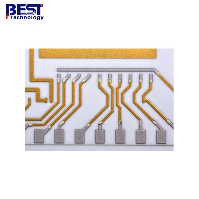
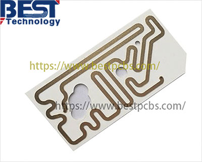
A lot of customers ask us what the biggest current his circuit can be carried, or how can I got a 6 Amps trace? We believe most of engineer design the thick film ceramic PCB, he will consider that, so we share information bellowing and hope it’ll be helpful for you.

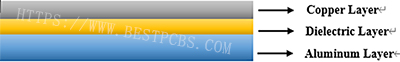
When you try to know current, you also need to know the watts of trace will be, and then need to know the power density of thick film ceramic PCB firstly. The power density for conductor itself should be limited to max 600 Watt/inch2 of conductor surface. And power density for an Al2O3 substrate should be limited to 8 Watts/in2 (for the total of all conductors on top of it).

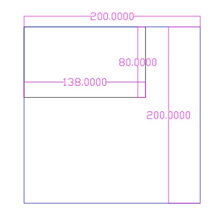
If you have a Ag conductor line of 0.3inch long, 0.010 inch wide (=30 square (0.3/0.01)), the surface area is 0.3 x 0.01 = 0.003 in2. This means the carrying powder P is limited to 600 (power density) x 0.003 (area) = 1.8 watts.

Assume conductor resistivity is 6mOhm/sq/12.5um (material P/N: ESL9562), the resistance value R = 30 sq x 6mOhm = 0.18 ohm.

Power = I2 x R, or I2 =Power/R=1.8/0.18 = 10, so the carrying current limit I = 3.16 amps. Or in a short equation,

I (amps) = line width (inch) x (power density)1/2 / (sheet resistance, ohm) 1/2

  1. If the trace keep 0.3 inch long, but change width to 0.02inch, (=15 square (0.3/0.02), the surface area is 0.3 x 0.02 = 0.006 in2. This means the carrying powder P is limited to 600 (power density) x 0.006 (area) = 6 watts.
    And resistance value for that trace will be 15 square x 6mOhm = 0.09 ohm, and then 3.6/0.09= 40, I=6.325 amps.
  2. If the trace width keep 0.01inch, but change line to 0.6 inch long (=60 square (0.6/0.01), the surface area is 0.6 x 0.01 = 0.006 in2. This means the carrying powder P is the same as 6 watts. (600×0.006).
    But the resistance value for that trace will change to be 60 square x 6mOhm = 0.36 ohm, and then 3.6/0.36= 10, I=3.16 amps. So you can see, it’s no useful to change the trace line.

So if you want to have bigger current for thick film ceramic PCB, then you need to increase the width of trace.

Hope above is clear for everybody. Please leave your comments on that power density of thick film ceramic PCB.

You may also like

2015 Chinese Spring Festival & Order Deadline

Tuesday, January 20th, 2015

Hello Everybody ,


Chinese Lunar New Year (Spring Festival) is coming soon. Thanks for your support in 2014 and always appreciated what you did for us! Looking forward to doing more with you in 2015!


Please to be noted that our company will be closed during the following period:


Closing Period: Feb 14th to Feb 28th , 2015

Resume on:  March 1st, 2015

As you know, production line before and after our long holiday will be extremely busy, and some worker will still home until Feb 12th, so lead time during this period will be at least 1-2 weeks longer than normal.

In order to avoid any potential delay for products delay, please consider our holiday arrangement and help to release order more early.

Here are deadline for orders which need to be shipped before our holiday:


FR4 PCB (without SMT)
1~2 Layer 4 Layer 6-8 layer 10 layer
New Samples 2-Feb-15 31-Jan-15 26-Jan-15 23-Jan-15
Volume production 31-Jan-15 29-Jan-15 27-Jan-15 25-Jan-15
Metal Core PCB (without SMT)
1 Layer 2 layers 4 layers
New Samples 31-Jan-15 26-Jan-15 21-Jan-15
Volume production 30-Jan-15 24-Jan-15 20-Jan-15
Ceramic PCB (without SMT)
1 Layer 2 layers 4 layers
New Samples 23-Jan-15 21-Jan-15 21-Jan-15
Volume production 21-Jan-15 20-Jan-15 20-Jan-15
For repeated order, deadline will be 1 days later.


Above lead time is subject to our confirmation after order receiving, as order on production line always increased so much.


Regarding SMT and other types of boards, please contact us for lead time.


For orders released late than above time, lead time will be postponed in March, 2015


We also have limited quick-turn service for 1-4 layers FR4 PCB. Contact us if any requirement.


Wish you a happy, healthy and prosperous New Year!

Best Technology always to be your best partner of FR4 PCB, Metal Core PCB, Ceramic PCB , SMT/PCBA in China.

You may also like

Happy 2015! Happy New Year!

Sunday, January 4th, 2015

2015 is coming now! Today (Jan 4th) is the first working day in China and of course 1st day working day in Best Technology.


When we look back to see what happened 2014, we grow up with the help of our customers, suppliers, friends, employees, step by step.


In new 2015, let’s work together, shoulder by shoulder, to achieve a brighter, more prosperous New Year! We can do nothing without you!


Always believe, Best Technology will be your long-period, reliable partner in China, for  Metal Core PCB, Ceramic PCB, FR4 PCB, rigid-flex circuits, various special circuit board, SMT Stencil, SMT and PCB Assembly.

Happy-New-Year-2015

Happy-New-Year-2015

You may also like