pcb
Home > Blog

Archive for 11 月, 2023

What is PCB Embedded Component Process?
星期三, 22 11 月, 2023

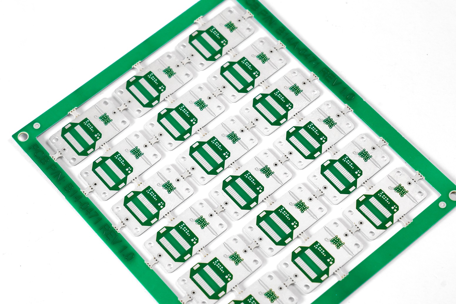
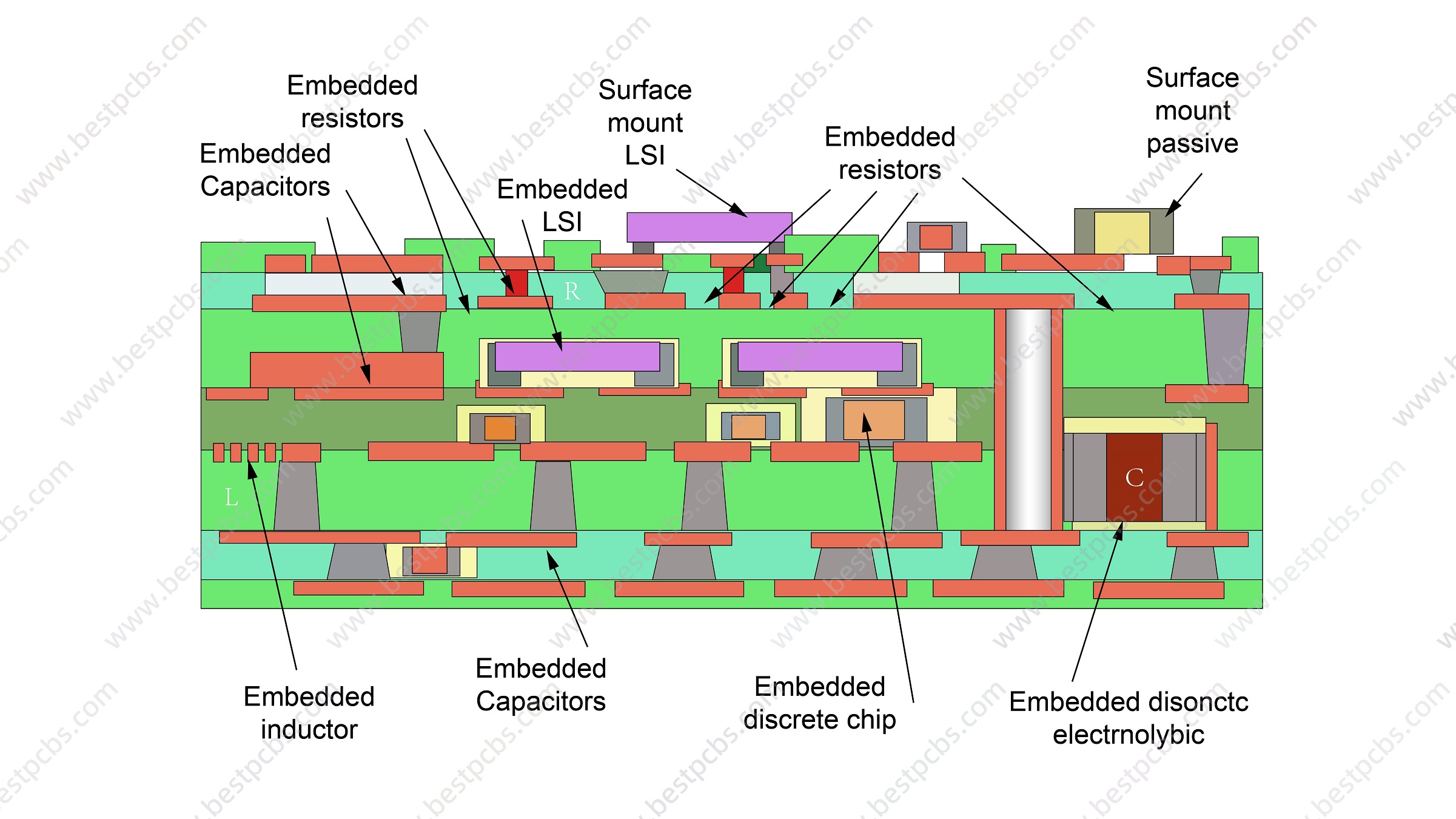
The resistance and capacitance buried in multi layers PCB process is a process of burying resistors and capacitors inside the PCB board. Usually, the resistors and capacitors on the PCB are directly soldered on the board through mounting technology, while the buried resistor and capacitor process is to embed the resistors and capacitors into the internal layer of the PCB board.

This kind of printed circuit board consists of a first dielectric layer, a buried resistor, a circuit layer and a second dielectric layer in order from bottom to top. Among them, the part of the buried resistor without a circuit layer on the buried resistor is covered with a polymer isolation layer, and the surface of the polymer isolation layer is roughened, the surface roughness Rz is bigger than 0.01 μm, and the thickness of the polymer isolation layer at the corners is at least 0.1 μm.

The printed circuit board of the utility model covers a layer of polymer isolation layer on the surface of the buried resistor, thereby protecting the buried resistor from being attacked and corroded by chemical chemicals during subsequent wet processes such as browning and super-coarseness, and improving the efficiency of manufacturing buried resistors. Resistor plate process capabilities further promote the application of buried resistive plates to inner layer buried resistors.

The advantages of the buried resistor and buried capacitor process include:

1. Space saving:

Since the resistors and capacitors are embedded directly into the internal layers of the board, space on the PCB board can be saved, making the entire circuit board more compact.

2. Reduce circuit noise:

Embedding resistors and capacitors into the internal layers of the board can reduce the electromagnetic interference and noise of the circuit and improve the stability and anti-interference capabilities of the circuit.

3. Improve signal integrity:

The buried resistance and buried capacitance process can reduce the transmission delay and reflection loss of circuit signals and improve the integrity and reliability of signal transmission.

4. Reduce the thickness of the PCB:

However, the buried resistor and buried capacitor process is relatively complicated in terms of manufacturing and repair, because the resistors and capacitors cannot be directly observed and replaced. In addition, the buried resistance and buried capacitance process is usually used in high-end electronic products, and the cost is relatively high.

When it comes to high-density circuit design, PCB buried resistance and buried capacitance technology has become a very useful technology. In traditional PCB layout, resistors and capacitors are usually soldered on the PCB surface in the form of patches. However, this layout method causes the PCB board to take up more space and may cause noise and interference on the surface.

The buried resistance and buried capacitance process solves the above problems by embedding resistors and capacitors directly into the internal layer of the PCB board.

The following are the detailed steps of the PCB buried resistor and buried capacitor process:

1. Make the inner layer:

When making a PCB board, in addition to the conventional layers (such as outer layer and inner layer), it is also necessary to make a separate inner layer specifically for buried resistance and buried capacitance. These internal layers will contain areas for buried resistors and capacitors. The inner layers are usually made using the same techniques as regular PCB manufacturing, such as electroplating, etching, etc.

2. Resistor/capacitor footprint:

Resistors and capacitors are packaged in a special package in the buried resistor and capacitor process so that they can be embedded into the internal layer of the PCB. These packages are usually thinned to accommodate the thickness of the PCB board and have good thermal conductivity.

3. Buried resistor/capacitor:

In the process of making the inner layer, the buried resistor and capacitor process is completed by embedding resistors and capacitors into the inner layer of the PCB board. This can be achieved through a variety of methods, such as using special pressing techniques to embed resistors and capacitors between inner layers of material, or using laser technology to etch holes in the inner layer material and then fill them with resistors and capacitors.

4. Connection layer:

After completing the inner layer of the buried resistor and buried capacitor, connect it to other regular layers (such as the outer layer). This can be achieved through conventional PCB manufacturing techniques such as lamination, drilling, etc.

In general, the buried resistance and buried capacitance process is a highly integrated technology that embeds resistors and capacitors in the internal layer of the PCB board. It can save space, reduce noise, improve signal integrity, and make PCB boards thinner and lighter. However, due to the complexity, the buried resistor and buried capacitor process is usually used in high-end electronic products with higher performance requirements.

You may also like

Do You Know How Does the ENEPIG Working for Wire Bonding Circuit Boards?
星期五, 10 11 月, 2023

The electronics industry has continuously pursued smaller and faster electronic products with increased functionality. To meet these demands, the electronic packaging industry has focused on developing more advanced packaging methods, aiming to increase the density of components on a circuit board while integrating multiple functions into a densely package.

The increasing density of packaging and interconnection has driven the progression of assembly methods from through-hole technology (THT) to surface-mount technology (SMT). Additionally, the use of wire bonding to connect chips to substrates has become more prevalent. The adoption of smaller interconnect pitches and chip-scale packaging (CSP) has further increased component density, while multi-chip modules (MCM) and system-in-package (SiP) have enabled the integration of more functions on a single package.

This post describes the key factors affecting the reliability of interconnections, with a particular focus on the specific properties of surface-treated wire bonding, emphasizing the selection of wire bonding surface treatments.

Selection of Surface Treatment for Wire Bonding

While electroless nickel gold provides excellent performance for wire bonding, it has three main drawbacks that hinder its application in cutting-edge technologies:

1. The relatively high demand for gold layer thickness leads to lengthy process costs.

2. Thick gold layers are prone to the formation of weak tin-gold intermetallic compounds (IMC), reducing the reliability of solder joints. To enhance solder joint reliability, alternative surface treatments may be used, but this increases additional process costs.

3. The electroplating process requires the use of electroplating lines, limiting the design freedom and wiring density of the packaging substrate.

The limitations posed by electroplated nickel-gold provide an opportunity for the adoption of chemical plating. The techniques of chemical plating include Electroless Nickel Immersion Gold (ENIG), Electroless Nickel Electroless Gold (ENEG), and Electroless Nickel Palladium Immersion Gold (ENEPIG).

Among these three options, ENIG is generally unproblematic due to its lack of high reliability in gold wire bonding properties (although it has been used in some low-end consumer products). On the other hand, ENEG shares the high production cost and presents complex challenges in terms of the manufacturing process, similar to electroplated nickel-gold.

ENEPIG was initially introduced in the late 1990s, its market acceptance was delayed until around the year 2000 due to fluctuations in palladium metal prices (which were inflated to unreasonable levels around 2000). However, ENEPIG can meet the requirements of many new packaging applications, providing reliable performance and conform to lead-free/ROHS requirements, with a recent strong surge in market demand.

In addition to the advantages in packaging reliability, the cost of ENEPIG is another benefit. With the recent rise in gold prices surpassing US$800/oz, it becomes challenging to control costs for electronic products requiring thick gold plating. The price of palladium (US$300/oz), relative to gold, is less than half, making palladium a cost-effective alternative with surface-related advantages.

Comparison of Surface Treatments

Up to now, for printed circuit boards accommodating fine-pitch QFP/BGA components, there are primarily four lead-free surface treatments:

Immersion Tin (IT)

Immersion Silver (IAg)

Organic Solderability Preservatives (OSP)

Electroless Nickel Immersion Gold (ENIG)

The table below compares these four surface treatments with ENEPIG. Among these surface treatments, none can simultaneously meet all the requirements of lead-free assembly processes, especially when considering multiple reflow experiences, pre-assembly shelf life, and gold wire bonding experiences. In contrast, ENEPIG offers good shelf life, solder joint reliability, gold wire bonding capability, and can serve as a touch button surface, providing surface-related advantages. Moreover, in the final gold replacement deposition reaction, the chemical palladium layer in ENEPIG works to protect the nickel layer, avoiding excessive corrosion during gold replacement.

(Table 1 – Comparison_of_Different_Surface_Treatment_Performances)

What Are Advantages of ENEPIG?

ENEPIG has several crucial advantages, demonstrating reliable solderability and gold wire bonding concurrently. The key benefits are outlined as follows:

  • Prevention of “Black Nickel Problem” – The absence of gold replacement attacking nickel on the surface prevents interfacial corrosion.
  • The chemical palladium layer acts as a barrier, preventing copper from diffusing to the surface, ensuring satisfactory solderability.
  • Palladium layer enable to completely dissolves in the solder, preventing the exposure of a high-phosphorus layer at the alloy interface. After the dissolution of the chemical palladium layer, the chemical nickel layer is revealed, forming a satisfactory nickel-tin alloy.
  • Capability to Withstand Multiple Lead-Free Reflow Cycles
  • Excellent Gold Wire Bonding Properties

These advantages make ENEPIG a preferred choice in various applications, ensuring reliable performance in both soldering and wire bonding processes while offering cost efficiency. As a one-stop PCB supplier in Asia, Best Technology possesses advanced technology and high-tech manufacturing equipment that can meet the “multi-variety, small volume, high quality, strong capability, short delivery” requirements. Welcome to contact us if you are going to find a reliable circuit board manufacturer.

You may also like