Archive for July, 2021

The way to add the mouse bite on the PCB Panel #Bestpcb

Saturday, July 31st, 2021

#Bestpcb #Best PCB

Maybe you’ve ever been recommended by your PCB manufacturer to add a mouse bite on the PCB edge?

But, what’s mouse bites?  Is it something about the Rat?

Of course not, it is kind of connection way for PCB Panel.

As you know, usually the Printed Circuits Boards are manufactured on a standard sized panel, and sometime, the panel will with sharp edges, and those sharp edges are often referred to as “mouse bites” and they are left over after depanelization.

mouse bite PCB depanelization Best Technology

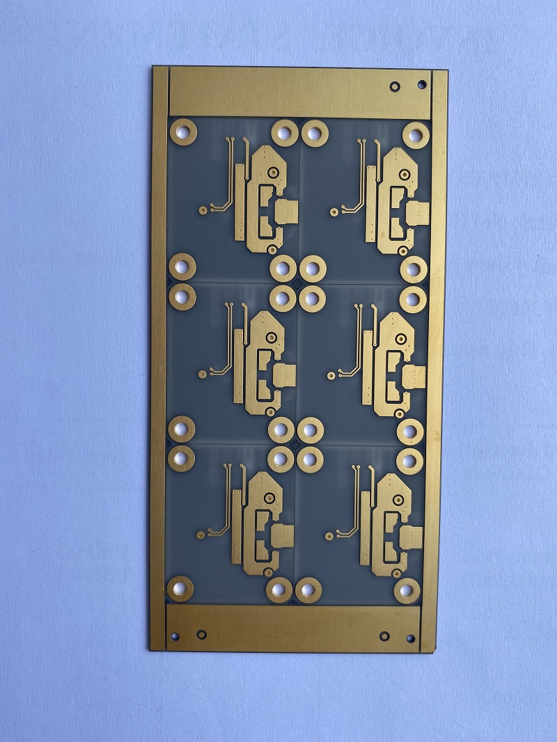
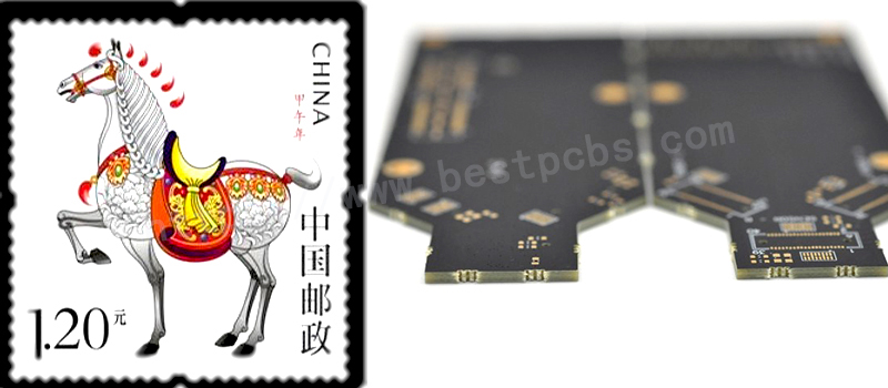
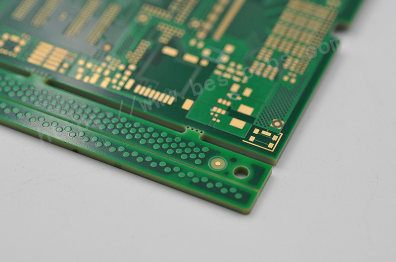
Mouse Bites usually presented as row of tiny holes on the board edge, just like the half holes around a stamp, which to connect and allow those small boards in an array.

mouse bite stamp holes on the PCB edge

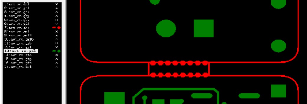
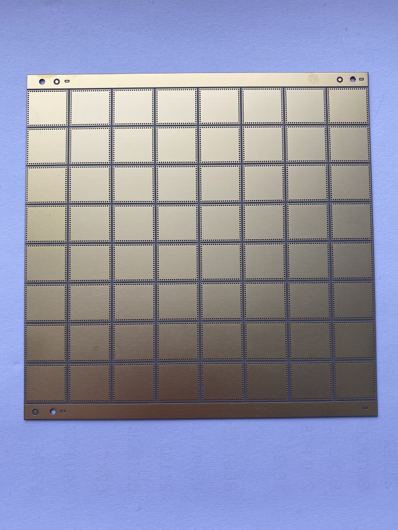
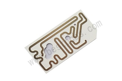
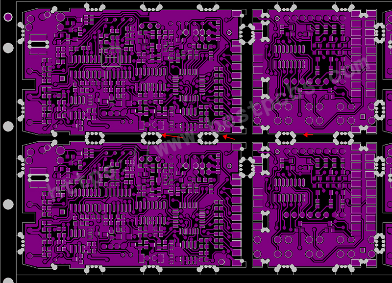
Here is the picture for you to see how the mouse bites presented on the Gerber drawing and what it is when it is finished.

Partial Effect drawing after Penalization: (the way of connecting bridge is used in the middle, this way can reduce the residue of burr in minimize)

Partial Effect drawing pcb panel
PCB panel mouse bite

Some People also called mouse bites as perforated breakaway tabs, it is designed for a better the purpose of the mouse bites is for a better grasp when mounted.

Here is the design rules if you need to add the mouse bites on your PCB panel.

  1. The distance between each single board need to arranged as 1.2mm and 1.6mm.
  • The distance between each holes need to be 0.2mm, the distance between holes center should be 0.75mm.
  • Need to add two rows, the mouse bites extend to 1/3 of the board, if there is a some circuits on the board edge, you will need to avoid it.
  • After adding mouse bites, the shapes of the two sides of the hole are connected, which is convenient for the production of gongs after work.

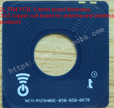
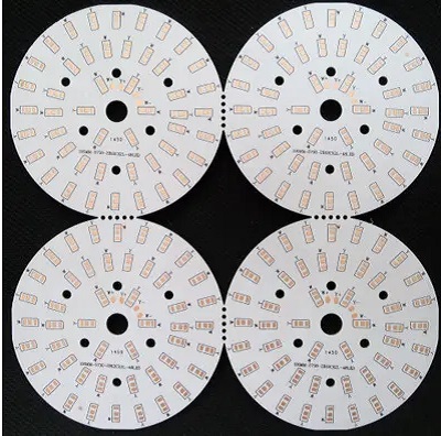
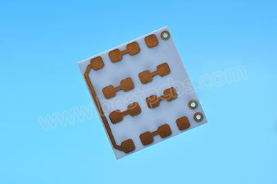
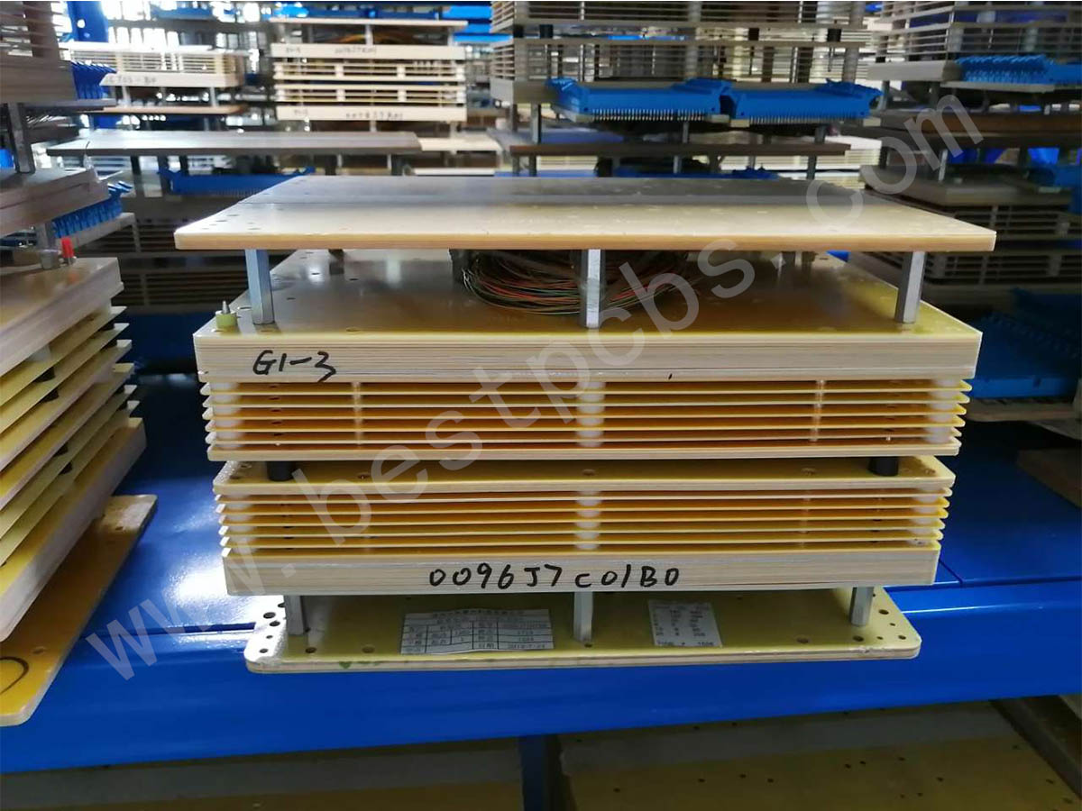
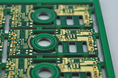
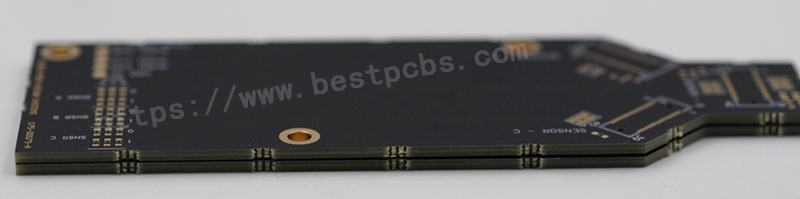
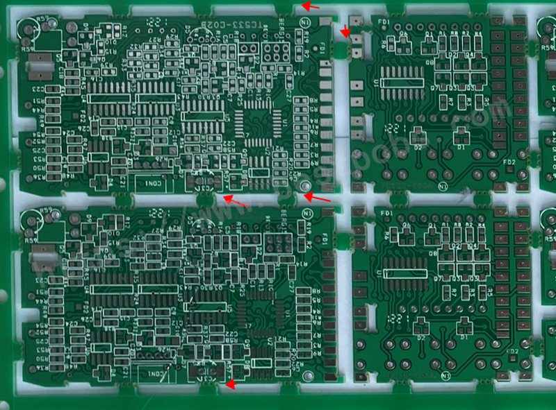
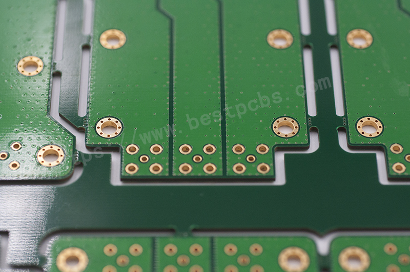
Here are some of our PCB with mouse bites for your reference.

mouse bite PCB Best Technology
PCB with mouse bit

If you want to add mouse bites on your PCB board, you are welcome to send us your request and we will help you make it on your PCB Panel.

You may also like

How to make Panel for MCPCB?

Friday, July 16th, 2021

Regarding all Metal core PCB required panelization, which needs to take into account how the boards are connected. There are two main connection methods for panel: Double face carved V-shaped groove (V-CUT), and the long slot plus a small circular hole (commonly known as stamp hole), depending on the shape of the PCB.

  1. V-CUT

V-CUT is to draw a slot at the junction of two boards, where the connection of the boards is relatively thin and easy to break. Currently SMT Board is widely used, characterized with neat and level edges after separation, which is recommended as priority.

V-cuts are generally straight lines, and there will be no complicated traces such as curved arcs, so pay attention to be in a straight line when making the panelization. Please also note the following two points.

â‘  The two sides of V-CUT line (top side and bottom side) require a no circuits area that is not smaller than 1mm, to avoid the damage circuits when separating.

② After cutting the V-shaped groove, the remaining thickness should be 1/4 to 1/3 of the total board thickness , which is not smaller than 0.4mm.

V-Cut
  • Stamp Holes/Mouse Bite

For irregular PCB boards, the shape of the board has curved corners, there will be many burrs if use V-cut. In this case the stamp hole connection would be the better choice.

  1. Panelization Rules:
  1. The spacing between the panel and the board is 1.2mm or 1.6mm.
  • The diameter of hole is 0.55mm, generally a row of 8 holes (Hole count depends on the design requirements, more holes can enhance the stability), the spacing of the two holes is 0.2mm.
  • The distance between the upper and lower rows of holes is 2mm, and 1/3 of the stamp holes enter the board. Pay attention to avoid the circuit on the edge of the board.
  • After adding the stamp holes, the shape of both sides of the hole need to be connected to facilitate the subsequent routing manufacturing.
  • The part picture after panelization.(Using the connection bridge in the middle, which can minimize the residual.)
Part Picture
  • The effect picture after panelization.
Stamp Holes

If you want to learn more about MCPCB design, welcome contact us.

You may also like

Laser drilling and cutting in the production process of ceramic circuit boards

Monday, July 12th, 2021

In the ceramic circuit board processing and production process, laser processing mainly includes laser drilling and laser cutting.

Ceramic materials such as alumina and aluminum nitride have the advantages of high thermal conductivity, high insulation and high temperature resistance, and have a wide range of applications in the fields of electronics and semiconductors. However, ceramic materials have high hardness and brittleness, and its molding and processing are very difficult, especially the processing of micropores. Due to the high power density and good directivity of the laser, lasers are generally used to perforate ceramic plates. Laser ceramic perforation generally uses pulsed lasers or quasi-continuous lasers (fiber lasers). The laser beam is focused on On the workpiece placed perpendicular to the laser axis, a laser beam with high energy density (105-109w/cm2) is emitted to melt and vaporize the material. An air stream coaxial with the beam is ejected by the laser cutting head to remove the melted material from The bottom of the incision is blown out to gradually form a through hole.

Due to the small size and high density of electronic devices and semiconductor components, the precision and speed of laser drilling are required to be high. According to the different requirements of component applications, electronic devices and semiconductor components have small size and high density. Due to its characteristics, the precision and speed of laser drilling are required to be high. According to the different requirements of component applications, the diameter of the micro-hole is in the range of 0.05 to 0.2 mm. For lasers used for ceramic precision processing, generally the focal spot diameter of the laser is less than or equal to 0.05mm. Depending on the thickness and size of the ceramic plate, it is generally possible to control the defocus to achieve through-hole punching of different apertures. For through-holes with a diameter less than 0.15mm, drilling can be achieved by controlling the defocus amount.

There are mainly two types method for cutting ceramic PCB: waterjet cutting and laser cutting. Currently, fiber lasers are mostly used for laser cutting. Fiber laser cutting ceramic circuit boards has the following advantages:

(1) High precision, fast speed, narrow cutting seam, small heat-affected zone, smooth cutting surface without burrs.

(2) The laser cutting head will not touch the surface of the material and will not scratch the workpiece.

(3) The slit is narrow, the heat-affected zone is small, the local deformation of the workpiece is extremely small, and there is no mechanical deformation.

(4) The processing flexibility is good, it can process any graphics, and it can also cut pipes and other special-shaped materials.

Al2O3 PCB with drilling
AlN PCB with drilling

 Under the development trend of light and thin, miniaturization, etc., the traditional cutting processing method has not been able to meet the demand due to the insufficient precision. Laser is a non-contact processing tool, which has obvious advantages over traditional processing methods in cutting process, and plays a very important role in the processing of ceramic substrate PCB.

Please contact sales@bestpcbs.com if you want to know more ceramic PCB.

You may also like

What is E-Tester for Printed Circuit Board?

Sunday, July 11th, 2021

When the bare Printed Circuit Board qty become volume fabrication, the PCB manufacture will not use the Probe flying tester to test the PCB circuit board. Best Tech will make new PCB test fixture to test the bare PCB, The electrical Test (E-test), which is the final electrical test to verify net continuity and the absence of shorts on the bare printed circuit boards (PCBs). In Best Tech PCB factory, we perform 100% electrical testing on all bare PCBs its facilities as per IPC-6012 class 2 standard. And from the following photo in computer, you can see it will show PASS for PCB.

in test

in test

To test the PCB boards, we require the NETLIST file. Normally we create a reference netlist file from the customer’s original Gerber files during PCB fabrication.

We always prefer to receive the CAD file based on the netlist for comparison. Since a CAD based netlist is generated before PCB routing, it provides another layer of checking (against the Gerber files). This allows us to catch any PCB faults introducing in the event of an error in the Gerber files. For full turnkey PCB assembly (PCBA service) projects, this helps to ensure that the PCB boards are 100% correct before any components are populated.

tester 2

tester2

Here are Best Tech E-tester Capabilities

Minimum Continuity Resistance0.1 Ohms
Maximum Test Voltage1000 Volts
Max Isolated Resistance25 M Ohm – 2 G Ohm
Electrical Test Pitch (Fixture)20mil(0.5mm)
Electrical Test Pitch (Flying Probe)4mil
Debug /check for missing pins: (Test fixture)10 minutes
Test time per board:40 seconds
Setup time:30 minutes

All points are tested simultaneously. However, this process involves set-up to create the fixture itself and additional costs associated with the cost of materials.

The electrical test fixture has a limited shelf life and repeat using times. For every PCB it will need a fixture and its custom-made for a customer only. Many other factories only store 2 years shelf life for electrical test fixtures, but Best Tech will store at least 3 years for customer.

In order to ensure the quality of fixtures and spare enough space to store fixtures, Best Tech leaves one floor to keep the fixture. See attached fixture photo.

tester 1

tester1

During the 3 years’ time, customer no need to pay the fixture charge again if the update is no update. The flexible test fixture shelf-life policy, it will help customer save the cost.

At the end of the PCB production process, we use electrical test to check the interconnectivity of the PCB is correct against the original board data.

Best Tech did the E-Tester to test the PCB 100% before delivery to customer, this makes Best Tech get highly comments from our customer on the world with good printed circuit board quality and best service. See the customer highly comments of Best Tech.

customer highly comments on our service

customer highly comments on our service

You are warm welcomed to contact Best Tech to discuss about the Printed Circuit Board (PCB).

You may also like