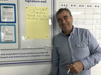
On Oct 14th, customer Oren and Amitay from Israel visited our company. They are very nice and smart, just arrived at our office without any more instruction. We’re old friends since 2011 but never meet each other in China. After drinking Chinese black tea, we had a delicious lunch: Chinese traditional Hot Pot and fried fish with red pepper.
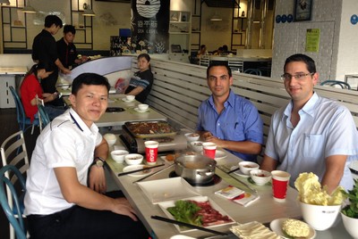
Hot pot & fried fish lunch
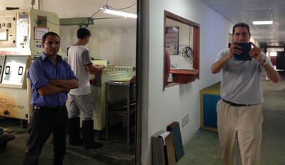
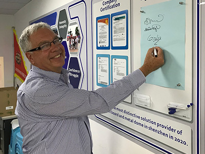
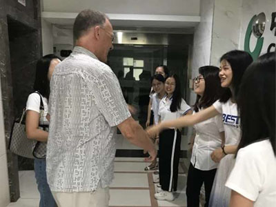
We also took photo with some of sales girls in office. You can see, how happy we are!
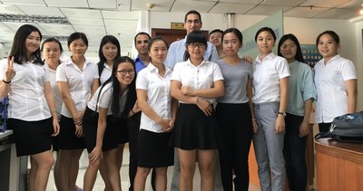
In office with sales girls
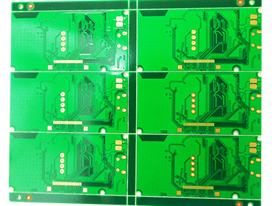
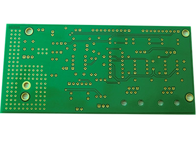
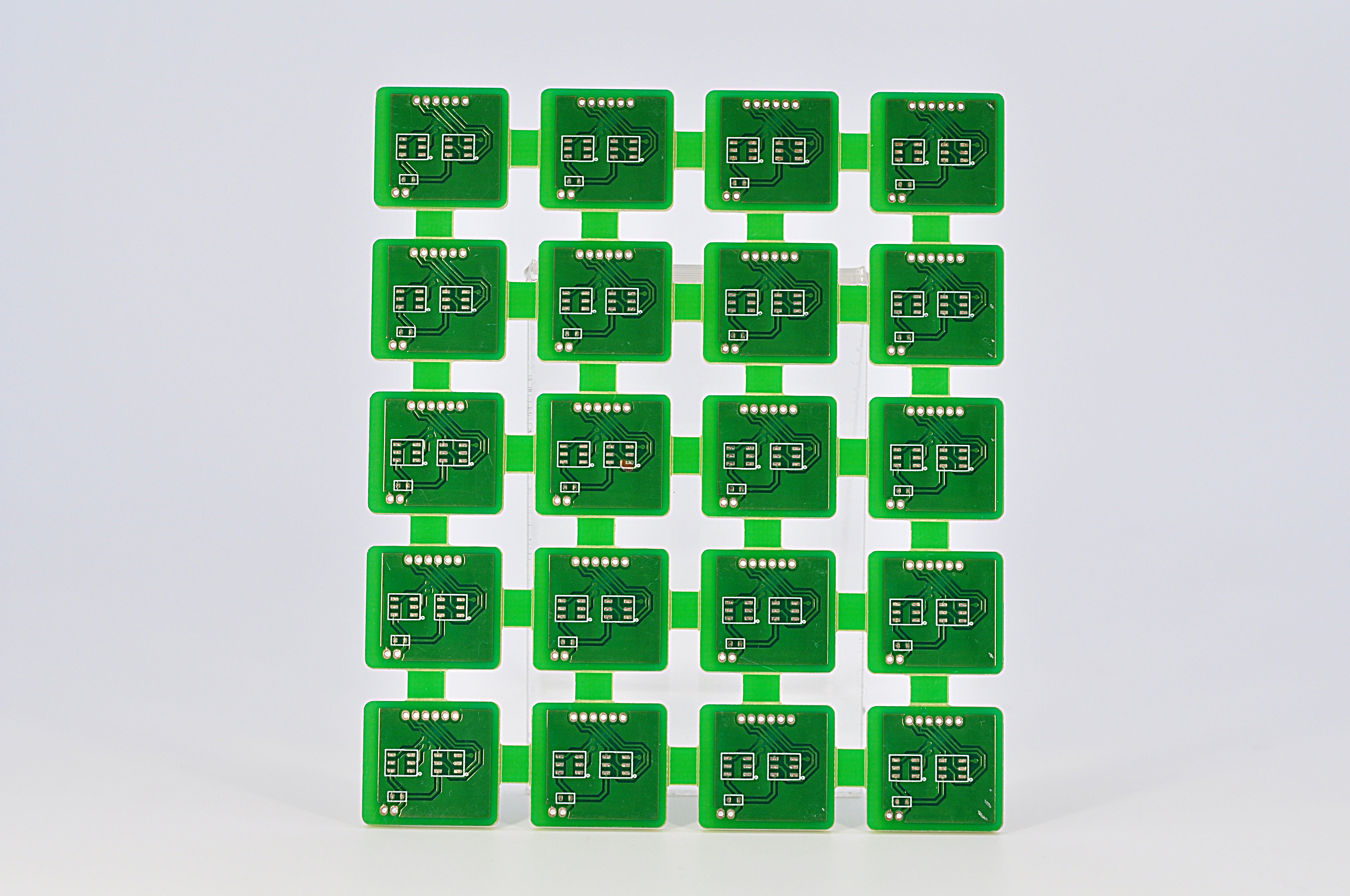
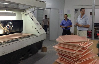
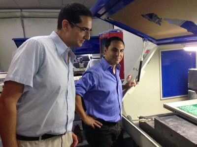
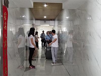
After that, they visited our Printed Circuit Board factory to visit whole PCB manufacturing process. From initial PCB raw material cutting, CNC drilling, exposure, etching, copper platting, soldermask & silkscreen printing, CNC routing, V-cutting, to final opening & shorting testing, flying probe testing, FQC and packaging. We also introduce our special board such as heavy copper PCB, extra thin PCB.
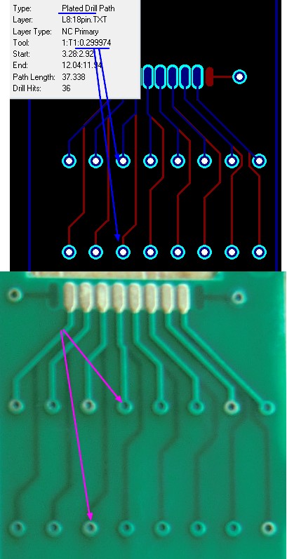
PCB raw material CNC drill (1st drilling, to make PTH (plating through hole)
PCB DES line (developing, Etching, stripping)
PCB CNC Routing & Milling
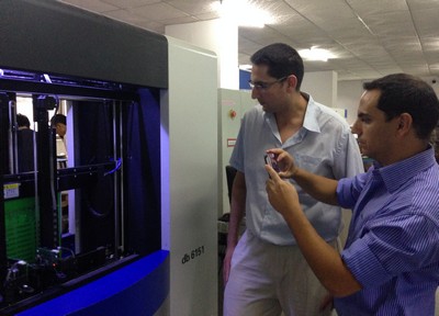
PCB flying probe testing to test PCB opening & shorting
After visiting whole process of FR4 Printed Circuit board and Metal Core PCB, they speak highly of us and also give us some suggestion to help us to improve our PCB manufacturing level and PCB quality. Thank you Oren and Amitay.
Looking forward to seeing you soon in Israel in 2017.

")

")