pcb
Home > Blog

Archive for 1 月, 2024

What’s the Role of MCPCB in Advancing Teeth Whitening Technology?
星期三, 31 1 月, 2024

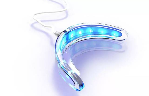
In the pursuit of brighter smiles, teeth whitening devices have become indispensable tools, utilizing various techniques to enhance dental aesthetics. Among these, light-based approaches, such as phototherapy and laser treatments, play a significant role. Interestingly, these advanced methods, including ultrasonic vibration, often rely on a crucial technological component – the Metal Core Printed Circuit Boards (MCPCB). In this blog, we will explore the concept of teeth whitening devices, the technology employed, and delve into why metal core PCB, particularly preferred for LED products, are integral in crafting efficient and reliable teeth whitening instruments.

(Teeth_Whitening_Devices_Illuminating_Smiles)

What is the Purpose of Teeth Whitening Equipment?

Teeth whitening devices are designed to improve the color of teeth, aiming for a whiter and brighter appearance. These devices apply various techniques, each contributing to the overall effectiveness of the whitening process. Notably, light-based methods have gained prominence, with two prominent technologies standing out: light phototherapy and laser treatments.

Light Phototherapy: This approach involves using specific wavelengths of light to activate whitening agents on the tooth surface. Patients wear protective eyewear while the device emits light, expediting the whitening process.

Laser Treatments: Similar to phototherapy, lasers target whitening agents, enhancing their efficacy. Typically conducted in professional dental settings, laser treatments offer precise and accelerated teeth whitening.

Ultrasonic Vibration: Some devices employ ultrasonic vibration, utilizing the principle of mechanical oscillation to enhance the penetration and effectiveness of whitening agents.

Why choose MCPCB for Teeth Whitening Devices?

Behind the scenes of these advanced teeth whitening technologies lies a critical component – the metal substrate. Often, LED products utilized in teeth whitening devices prioritize metal substrate for their construction. But what exactly is a metal core PCB, and why is it the preferred choice?

Understanding Metal Substrates: The Foundation of Reliability

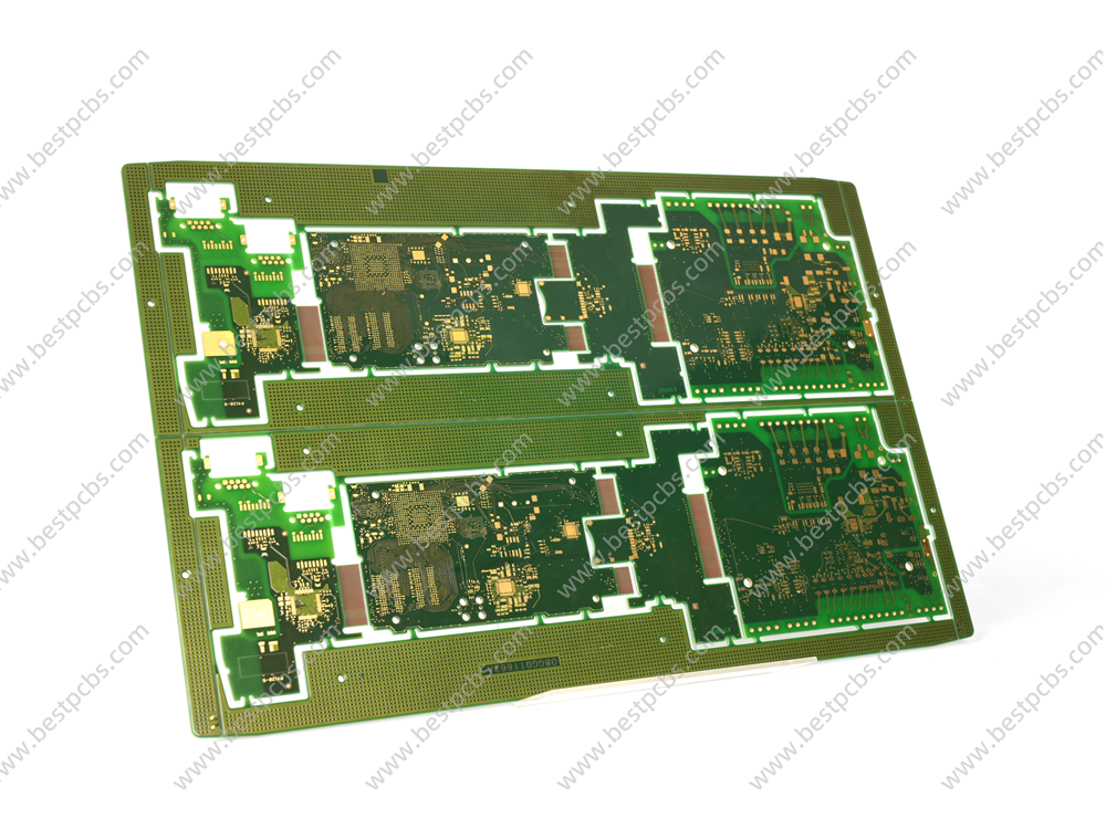
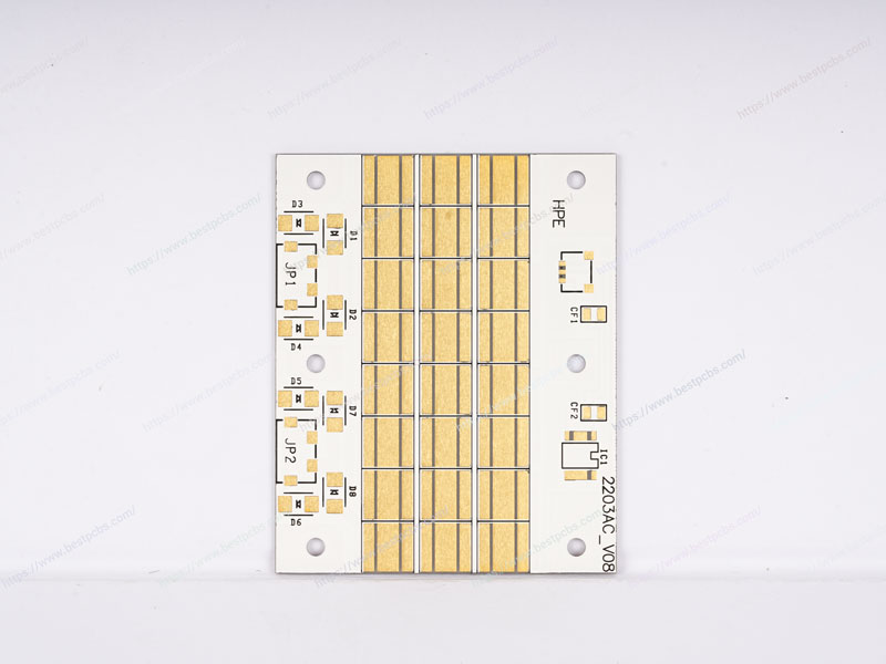
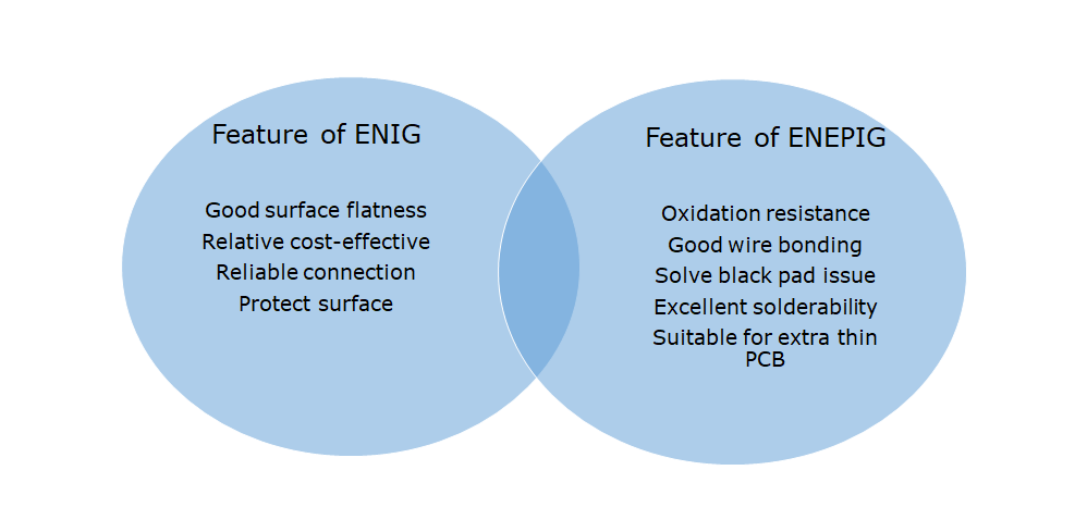
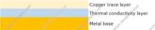
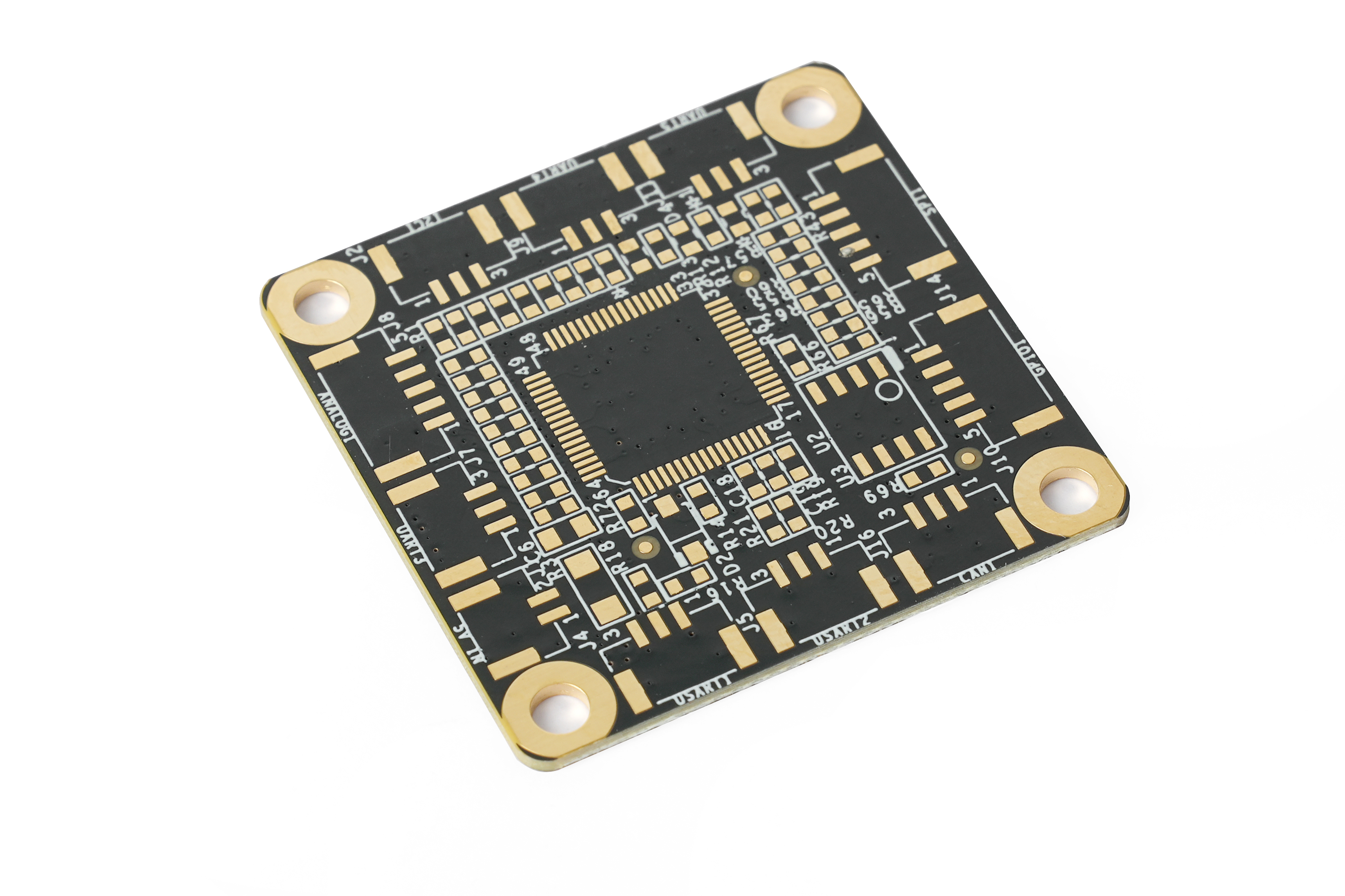
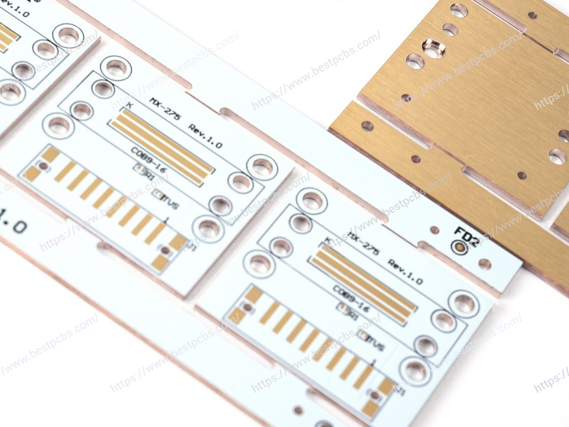
MCPCB (Metal Core Printed Circuit Board) is a specialized type of printed circuit board characterized by the presence of a layer of metal with excellent thermal conductivity on the substrate. Typically, MCPCBs are composed of a metal core, insulating layer, and copper foil, with the thermal conductivity of the metal core being a significant distinction from conventional FR4 circuit boards.

Key Features of Metal core PCB: Unveiling secret

Superior Thermal Conductivity: Teeth whitening devices often utilize technologies such as light or laser, generating heat during operation. the metal core of MCPCB exhibits exceptional thermal conductivity, effectively dissipating heat to prevent overheating. This property ensures efficient heat dissipation, a critical factor in devices requiring prolonged operation, such as teeth whitening instruments.

Regarding the metal base of MCPCB, aluminum base or copper base are commonly used for MCPCB, it’s also help to make the good heat dissipation than FR4PCB, like aluminum base has 205W/m.k and copper base has 398W/m.k, as you can see the thermal conductivity of copper base is better than aluminum base, so if your products need a more higher heat dissipation, welcome to consider copper core PCB, but please noted that copper is expensive than aluminum, which material depends on your requirement.

As thermal conductivity, it’s more important in MCPCB, since the higher the thermal conductivity, the higher the ability of heat dissipation, for now, the highest thermal conductivity is 8W/m.k in Best Technology, but for normally, 1W/m.k, 2W/m.k and 3W/m.k is enough for LED products.

Enhanced Heat Dissipation: MCPCB excels in dissipating heat, preventing overheating during prolonged use. This characteristic is crucial in teeth whitening devices, where maintaining a balanced thermal environment is essential for both device performance and user comfort.

Mechanical Strength: Metal substrates exhibit high mechanical strength, withstanding the rigors of assembly and use. This durability ensures the stability and reliability of the devices over time.

Structural Robustness: Teeth whitening devices may experience mechanical stress during operation, including vibrations or movements. The metal core of MCPCB provides additional structural support, enabling the device to withstand mechanical pressures and enhance overall durability.

Ideal for LED Products: MCPCBs are often the preferred choice for LED products due to their excellent thermal management and structural stability. LED-based teeth whitening devices benefit significantly from MCPCBs, ensuring the longevity and reliability of the LED components.

Why Metal Substrates for Teeth Whitening Devices?

The choice of metal substrates in teeth whitening devices, especially those employing LED technology, is strategic. The need for a material that offers robust electrical conductivity, efficient heat dissipation, and structural integrity aligns perfectly with the characteristics of metal substrates. In LED products, where precision and reliability are paramount, metal substrates emerge as the preferred foundation.

In conclusion, the convergence of advanced technologies for teeth whitening and the reliability of metal substrates highlights the intricate dance between innovation and foundational support. As we continue to seek brighter smiles through cutting-edge dental aesthetics, the role of metal substrates remains fundamental, quietly empowering the devices that illuminate our smiles and boost our confidence.

Best Technology has involved in MCPCB industry from 2006, over 17years, we can help to design, manufacturing and assembly, providing one-step service for our customers, welcome to share your drawing or idea to us, we will back you the best solution!

You may also like

How Does the Ceramic PCB Works in IGBT Modules?
星期五, 19 1 月, 2024

IGBT (Insulated Gate Bipolar Transistor) is a bipolar junction transistor (BJT) with a MOS gate, or we can say that an IGBT module is a combination of BJT and MOS module. Despite its small size, the IGBT chip can control the transmission of electrical energy. It can switch the current 100,000 times within 1 second under an ultra-high voltage of 650 million volts.

What is the Working Principle of IGBT?

IGBT combines the features of a transistor and a switching circuit, making it a new type of electronic component that can control current efficiency. Its structure allows it to achieve current control from turn on to off without generating excessive leakage current, as well as not affecting the operation of other circuits.

The working principle of IGBT modules including two parts – the current control of MOS gate and BJT transistor. When the voltage of MOS gate changes, it affects the conduction of the transistor, thus controlling the flow of current. When the BJT comes into play, it controls the flow of current, so that improve the working efficiency of the IGBT.

(Working_principle_of_IGBT)

How Does A Ceramic PCB Protect IGBT Modules from Overheat?

As you know, IGBT modules have been applied for many years in various industries such as automotive, industrial, aerospace, consumer electronics, and more. However, optimizing the thermal dissipation of IGBT packaging is crucial to enable the modules to operate at higher power conditions. If heat dissipation is improved, IGBT modules can be used in more advanced applications.

You might be wondering how much heat does an IGBT module generate during running? It’s equivalent to the heat produced by 100 electric furnaces. This substantial amount of heat must be dissipated immediately from the IGBT chip, that’s why the ceramic circuit board stands out.

(Ceramic_pcb_with_DPC_technology)

In IGBT modules, ceramic PCBs are placed beneath the IGBT chip, or we can say the chip is assembled on the ceramic circuit board. The ceramic PCB connects and supports the chip, rapidly dissipating heat to the outer package. This method protects the chip from the adverse effects of heat.

Why ceramic PCBs Are Suitable for IGBT thermal dissipation?

Ceramic materials exhibit excellent thermal dissipation and electrical insulation properties. Unlike aluminum metal core PCBs, ceramic PCBs do not use insulation layers that hinder heat dissipation. In the manufacturing process of ceramic PCBs, copper foil is directly bonded to the ceramic substrate under high pressure and temperature (it depends on the different technology and different copper thickness). During PCB manufacturing, IGBT and other components are mounted on the circuit board through assembly technology.

Ceramic materials have extremely high insulation capabilities, enduring breakdown voltages up to 20KV/mm. At present, there are three ceramic materials that can be used for IGBT modules, they are 99% or 96% Alumina (Al₂O₃), Aluminum Nitride (AlN), and Silicon Nitride (Si₃N₄).

The thermal conductivity of alumina PCB is 15-35W/mK, aluminum nitride PCB is 170-230W/mK, and silicon nitride PCB is 80+W/mK. In contrast, aluminum core circuit boards only have a thermal conductivity of 1-12W/mK.

Applications of Ceramic PCBs in IGBT Packaging

Alumina PCBs are the most commonly used circuit boards in IGBT modules due to their lower cost. But if IGBT modules have higher power or precision requirements, AlN ceramic PCBs and Si3N4 PCBs are the most suitable choices. Because they have higher thermal dissipation and thermal expansion coefficients (CTE) close to semiconductors. Since different ceramic substrate has different features, the uses of ceramic PCB should depend on the specific requirements of IGBT modules.

In addition, with the development of Silicon Carbide (SiC) and Gallium Nitride (GaN) materials, they are starting to be used for IGBT chips due to their high-frequency, high-power, and high-temperature characteristics. Maybe in the future, aluminum nitride PCBs and silicon carbide PCBs will be increasingly applied to high-power IGBT modules in high-density three-dimensional packaging.

Common Properties of Using Ceramic Circuit Board

  • Excellent thermal conductivity and voltage resistance of ceramic substrates.
  • Copper trace layers has extremely high current-carrying capacity.
  • Strong adhesion and reliability between circuit layers and ceramic substrates.
  • Good soldering performance, suitable for wire bonding.
(Ceramic_PCB)

How to Solve the Overheat Issues in IGBT?

Though the ceramic PCB is good at heat dissipation, there still some overheat occasions happened if small power or long-time operation. Here we summarized some solutions for such issues.

1. Clean the heat sink to ensure tight contact between the IGBT and the heat sink.

2. Clean the fan, including the fan blades and lubricate the bearings if needed.

3. Clear the airflow path of the fan.

4. Replace with higher power IGBTs, ensuring the withstand voltage is not lower than the original IGBT’s value.

Above all are the information that we’d shared, welcome to contact us if you want to know more. Best Technology is a historic company which has over 17 years PCB manufacturing experience, here you can enjoy the one-stop ODM & OEM service, one-to-one after sales, quick delivery and high-quality products.

You may also like

Semi-Flexible PCBs: An Amazing Design in Electronics
星期二, 9 1 月, 2024

In the realm of advanced electronic design, Semi-flex PCBs stand out as pioneering solutions. Leveraging specialized FR-4 materials and employing a distinctive manufacturing method, they ingeniously combine the flexibility of a flexible circuit with the convenience of easy installation.

(Semi_flex_PCB)

Do you know what’s Semi-flex PCB?

A Semi-Flexible PCB (Printed Circuit Board) is a type of PCB that offers a compromise between rigid and flexible circuit boards. It incorporates elements of both rigid and flexible PCBs, allowing it to bend to some extent while still maintaining a degree of stiffness. This innovative flex-to-install design not only ensures cost-effectiveness but also opens up a realm of possibilities for diverse applications, making Semi-flex PCBs a versatile and economical solution in the ever-evolving landscape of electronic design. Embracing cutting-edge technology and adaptability, these boards exemplify the ongoing commitment to pushing the boundaries of innovation in electronic engineering.

(Semi_Flex_PCB_detail_1)

Vital Features of Semi-flexible PCBs

In our more than 17 years of experience in the PCB manufacturing field, we take pride in delivering Semi-Flexible PCBs that meet the highest standards of quality and performance. we are happy to share some the key features of our Semi-Flexible PCBs we made:

Flexibility and Bending Capability: The semi-flexible nature of these PCBs allows for bending and shaping, making them suitable for applications with space constraints or those requiring unique form factors.

Reliability: Despite their flexibility, our Semi-Flexible PCBs maintain high levels of reliability and performance. They are designed to withstand bending without compromising the integrity of the circuit.

Space Optimization: The ability to conform to three-dimensional shapes enables better use of available space, making these PCBs ideal for compact electronic devices and innovative product designs.

(Semi_Flex_PCB_detail_2)

As we move forward, we invite you to explore the possibilities that Semi-Flexible PCBs offer and to partner with us in shaping the future of electronic engineering. Together, let us continue to embrace the spirit of innovation and unlock new horizons in the dynamic and rapidly advancing field of technology. Trust Best Technology, we are the BEST!

You may also like

What Are Differences of ENIG VS ENEPIG in PCB Manufacturing – Series 2
星期二, 2 1 月, 2024

In our last blog, we simply introduced ENIG surface treatment in PCB manufacturing, and this time, we will share more information about the comparison of ENIG and ENEPIG.

What is ENEPIG Surface Treatment?

ENEPIG stands for Electroless Nickel Electroless Palladium Immersion Gold. This type of metal coating on the PCB pad surface consists of three layers—nickel, palladium, and gold. Apart from protecting the copper surface from corrosion and oxidation, the ENEPIG surface treatment is also suitable for high-density SMT (Surface Mount Technology) designs.

For its manufacturing process, manufacturers begin by activating the copper surface, followed by depositing a layer of electroless nickel, then a layer of electroless palladium, and finally, a layer of immersion gold. The process is somewhat similar to the one they follow in the ENIG process, but adding a palladium layer to the ENIG technology. The palladium layer not only improves the surface protection of the PCB, but also prevents nickel from deteriorating and inhibits interactions with the gold layer.

Pros of ENEPIG Surface Treatment

  • Reduce the black pad issues
  • Excellent solderability and high reflow soldering performance
  • Provide high-reliable wire bonding capability
  • High-density design available
  • Meet the miniaturization standards
  • Suitable for extra thin PCBs

Cons of ENEPIG Surface Treatment

  • Expensive than ENIG process
  • Thicker palladium layer will decrease the effective of SMT soldering
  • Longer wettability time

What are the Differences Between ENIG and ENEPIG?

The main difference between ENIG and ENEPIG is the palladium layer. This is the extra layer that added in ENEPIG process, which provides high oxidation resistance, enhance the electrical performance of the surface cleanliness and improve the abrasion resistance of the PCB surface. However, the palladium layer also increases the cost of manufacturing.

Additionally, the inconsistent surface cleanliness of ENIG, resulting from low solder joint reliability, particularly in gold wire bonding, is a concern. Extra procedures are also required to prevent nickel corrosion in ENIG. When considering it into manufacturing, the ENIG is well-suited for lower-end electronic products.

(ENIG_VS_ENEPIG)

The Considerations of Selecting ENIG or ENEPIG Surface Finishing

Though both two surface treatments offer excellent electrical performance and heat dissipation properties, there are still some conditions that need to consider when choose them.

  • Budget

Cost is an important factor when choose a suitable surface treatment. As we explain above, ENEPIG is expensive than ENIG, if you are trying to find a relative cost-effective coating, then ENIG is the best choice.

  • End-applications

The end-applications or finished products also determined the selection of surface finishing. For example, if your PCB will be used in high temperature applications, ENIG would be the better one since it can withstand high temperature.

  • Flatness

Many traditional surface finishes have poor flatness and smoothness, this brings the big challenge of small-size components mounted. Especially for those fine-pitch components like BGA, an uneven surface can result many problems. However, both ENIG and ENEPIG offer highly smooth surface finishes, forming thin and uniform layers on the solder pads.

  • Bonding demand

ENEPIG provides the optimal choice for wire bonding due to its highly smooth surface finish, which enhances wire bonding capabilities.

  • Environment-friendly

Some traditional surface treatments contain hazardous substances, making them non-compliant with RoHS requirements. Both ENIG and ENEPIG made by Best Technology are fully RoHS compliant and lead-free, so you are don’t worry about the environment unfriendly.

At the end, the choice between ENIG and ENEPIG surface treatments in PCB manufacturing involves a careful consideration of various factors. While both options offer excellent electrical performance, heat dissipation properties, and compliance with environmental standards like RoHS, specific project requirements and priorities will guide the decision-making process. If you are still confuse about the selection of surface treatment, welcome to contact with us, Best Team will give you a best solution that can meet your specific demands and save money for you.

You may also like

Why Thermal Conductivity Layer is Important in Aluminum PCB?
星期二, 2 1 月, 2024

In the aluminum PCB design, people always mention the thermal conductivity value. Do you know what about thermal conductivity and you know what is the role of this layer in the aluminum core circuit board? Welcome to keep reading if you are interested in it.

(1_layer_aluminum_pcb)

What is thermal conductivity?

Thermal conductivity is a physical value signifies the capacity of a material to allow heat flow per unit area through it in a unit of time. A higher thermal conductivity indicates better heat conduction for the material. In the field of heat generation and thermal management products, thermal conductivity is a crucial parameter as it relates to the product’s heat dissipation capability and stability. In the structure of aluminum, the thermal conductivity layer is always stand between the copper circuit layer and base material, so that the heat generated by product can be transfer quickly to outside.

(Stack_up_for_1_layer_aluminum_PCB)

Significance of Thermal Conductivity in Aluminum PCBs

Aluminum substrates are commonly used materials in heat dissipation and thermal management products. Their thermal conductivity is a vital element evaluated heat dissipation properties typically in W/m·K. It can be understood as the material’s heat transfer rate, i.e., the amount of heat conducted per unit time. Specifically, assuming the same amount of heat is conducted in aluminum substrates and other materials, the conduction rate of aluminum substrate will be faster over a certain period. This implies that aluminum substrates can transfer heat more quickly from the heat source to the external environment, achieving efficient heat dissipation.

Impact of Thermal Conductivity on Heat Dissipation Products

The primary function of thermal management products is to dissipate heat. How does thermal conductivity specifically affect them? Let us dive into from below aspects:

1. Thermal Conductivity Value

A higher thermal conductivity leads to better heat dissipation capability, as it can achieve faster transfer of heat from the heat source to the environment. Therefore, thermal conductivity of aluminum substrates plays a crucial role in the heat dissipation products, such as the LED lights, industrial power devices, automotives. At Best Technology, the thermal conductivity we used for aluminum PCB always is range from 1.0 to 3.0W (thickness=75-200um). Different thermal conductivity value has its own thickness.

2. Product Stability

The stability of a product also depends on its thermal conductivity. According to our 17+ manufacturing experience, insufficient thermal conductivity in heat dissipation products may result in overheating during prolonged operation, potentially shortening the product’s lifespan. Let me take a simple example, assume your mobile phone is under long time playing games, then it will generate many heats, finally causing the overheating phenomenon. And this will shorten its lifecycle if you always do like that.

(Single_sided_4_layer_aluminum_PCB)

When it comes to thermal conductivity selection, there is a big misunderstanding is that some may believe that higher thermal conductivity in aluminum substrates is always better. However, this is not entirely accurate. While higher thermal conductivity is generally favorable, it does not mean that aluminum substrates with the highest thermal conductivity are suitable for all heat dissipation applications. In specific use cases, it is essential to choose the appropriate thermal conductivity for aluminum substrates based on actual requirements to achieve the optimal heat dissipation effect.

By the way, if you want to choose higher thermal conductivity value, ceramic PCB is a better choice, which can achieve 24W or more. It mainly depends on its ceramic substrate material, like the Al2O3 thermal conductivity value is around 24W~28W/m-K, while AlN enable to reach 150W~240W/m-K.

Conclusion

All in all, to ensure optimal heat dissipation effects and stability, it is crucial to choose the right thermal conductivity for aluminum substrates based on actual needs. The careful consideration of thermal conductivity values in aluminum PCBs is integral to the longevity and performance of heat dissipation products, emphasizing the importance of informed selection in the pursuit of effective thermal management.

Best Technology is an expert in metal core PCB manufacturing, we have strong R&D team and full-experienced employs that can provide with you the best metal core PCB solution. Welcome to contact us at sales@bestpcbs.com if you want to know more.

You may also like

What Are Differences of ENIG VS ENEPIG in PCB Manufacturing – Series 1
星期二, 2 1 月, 2024

Surface treatment also called surface finishing, it is a protective layer that through coating a layer of metal organic material on the surface of printing circuit boards (PCBs). Apply a layer of surface treatment enable to protect pads from scratches and oxidation, as well as improve the solderability of components mounting. ENIG and ENEPIG are the two common high-reliable surface finishing types in the circuit board manufacturing, they are not only for FR4-PCB, but also available in ceramic PCB, flex circuits and rigid-flex PCB. Today, Best Team would like to sharing information about ENIG and ENEPIG, and explore the differences between them.

(Assembled_PCB)

How to Select the Right Surface Treatment for Your PCB?

With the rapid development of electronics, there are various of PCB types that can be used in electronic devices, and at the same time, there are also increasingly more surface treatment technics available for selection. Until now, the common surface treatments are OSP, HASL, Immersion Silver, Gold Plating, ENIG and ENEPIG. Each of these surface treatments has its own advantages and disadvantages, so it is necessary to choose the most suitable one for a particular application. The selection of surface finish needs to take into account factors such as cost, application environment, fine-pitch components, the use of leaded or lead-free solder, operating frequency, shelf life, drop and impact resistance, volume and throughput, as well as thermal resistance.

With PCBs trending towards micro-vias and finer traces, and the drawbacks of HASL and OSP, such as flatness and flux elimination issues, becoming more pronounced, the demand for surface treatments like ENIG continues to grow. In addition, black pad is a major weakness of ENIG while ENEPIG enable to solve it very well, making it a preferred choice for those PCBs need to wire bonding.

What is the ENIG Surface Treatment?

ENIG, its full name is Electroless Nickel Immersion Gold, is also known as chemical gold or immersion gold in the electronics industry. This type of surface treatment provides two metal layers—gold and nickel—that manufacturers deposit them on the surface of PCB pads sequentially. This surface finish is a selective surface finish, meaning that certain specific pads may have ENIG surface finish, while others may have different types, such as OSP, HASL, or immersion tin. Here are the main processes of the ENIG coating:

  • Copper activation

In this step, manufacturers will active the copper layer through cleaning process, this way can help to remove the dust and oxides residual on the surface, but also remove any gases or air trapped in the perforations (holes) of the PCB by wetting the surface. Next, micro-etching the PCB surface using substances like hydrogen peroxide or sulfuric acid.

  • Electroless nickel

This process is to coat a layer of nickel on the active copper layer by electroplating. The nickel layer serves as a protective layer or inhibitor, which prevent the copper reactive with other elements.

  • Immersion gold

Immersion gold is the last step of whole ENIG process, immersing the PCB into a mixture, oxidizing the nickel surface, generating nickel ions, and then reducing gold from the mixture. The reduced gold forms a metallic coating to protect the nickel surface. This is the whole process of coating ENIG surface treatment.

(PCB_with_ENIG_surface_treatment)

Advantages of ENIG

  • Surface flatness – good for fine-pitch and small size components like BGA.
  • Suitable for press-fit components since it provides a reliable connection for electrical testing.
  • Suitable for wire bonding and gold-fingers connectors.
  • Cost-effective compared with ENEPIG

Disadvantages of ENIG

  • Black pad issues.
  • Varied coating thickness because of the uncontrolled nickel plated and immersion gold.
  • Poor wettability during PCB assembly.

All in all, ENIG is a good option if you want to mount fine-pitch components on the PCB surface or if you are considering its use in plug-and-pull devices such as WIFI interfaces. In our next blog, we will introduce ENEPIG surface treatment, including its pros & cons and the differences between ENIG and ENEPIG. Pay attention to our news or contact us directly if you want to know more.

You may also like