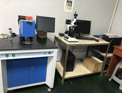
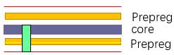
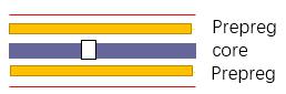
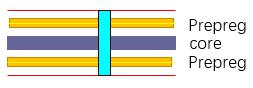
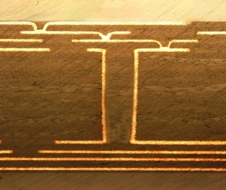
HDI abbreviation means High Density Interconnect. HDI PCBs have extremely density trace spaces and lines, micro vias under 0.25mm(10mil), smaller pads and higher connection pad density. See the photo of HDI board laser drill& prepreg thickness ratio.
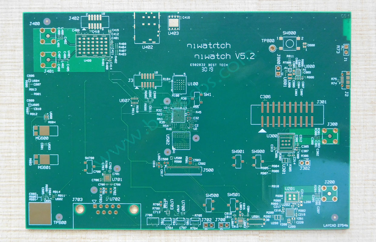
It is very helpful in enhancing electrical performance and HDI PCB use for high-end products and HDI PCB is regularly used in 4G network communications, medical, Military and Aerospace. See the HDI board which Best Tech made for customers.
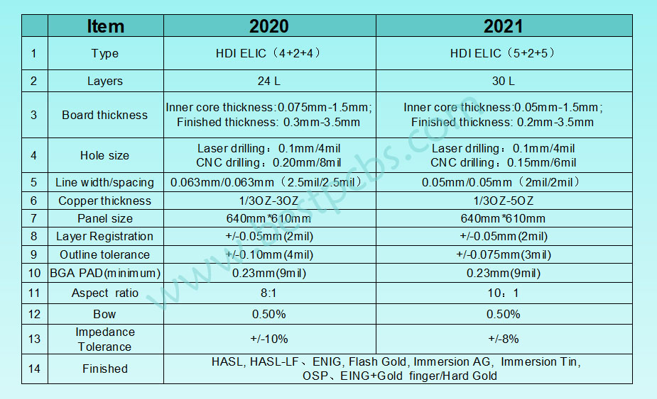
HDI PCB is the better option for high-layer count and costly laminated boards. Due to the increasing complexity of design structures laminate, the Blind vias and Buried vias are increasingly used in high-density circuit boards (HDI PCB board). Best Tech always improved manufacture capability for HDI, following production capability of the comparison for 2020 and the capability which Best Tech want to achieve at year 2021.
Following is the advantages to use an HDI PCB
The common reason for using HDI technology is a significant increase in packaging density. In addition, overall space requirements are reduced will result in smaller board sizes and fewer layers.
1.Denser trace
2.More stable performance
3.Reduce interference inductance and capacitance effects
4.Improve signal integrity in high-speed design
5. Reduce frequent relocation of components
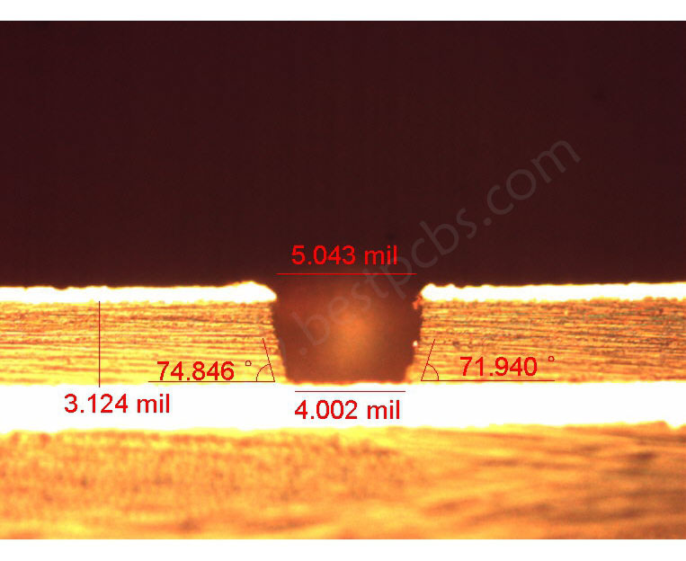
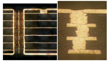
What’s mean for a blind via hole?
It is a hole runs from an outer layer, but not through the entire PCB. These holes can be drilled mechanically or using laser technology.
And what’s mean for a buried via hole?
This is a hole that runs between one or more inner layers. They are normally mechanically drilled.
By the way, we would like to make some explain for the through via hole, see attached photo to know the detail.
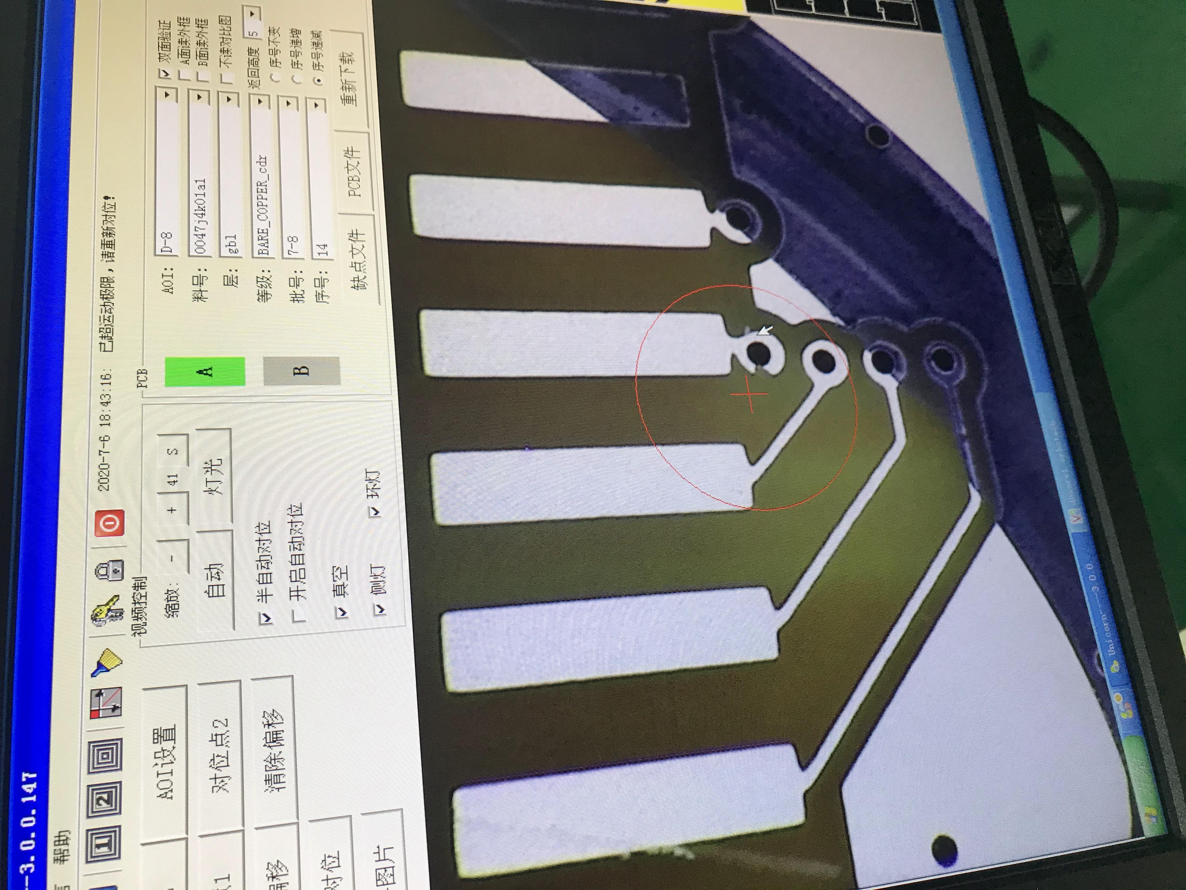
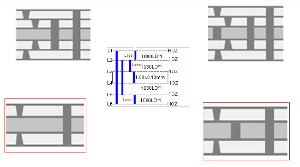
Do you want to know the different types for HDI PCB boards?
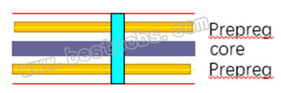
The following photos mainly shows the different laminate structures available from Best Tech for HDI PCB for prototype and mass production.
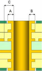
What is the minimum pad size of hole on the outer and inner layer?
This is different from manufacturer to manufacturer, but in general you can say that the majority of manufacturers can produce them as follows:
AÂ = 0.10 mm
BÂ = 0.15 mm
CÂ = 0.20 mm
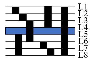
Finally, here is an 8L HDI FR4 PCB which we made for our customer at June. See the stack up information.
Surface finish: ENIG(2uâ€)
Features
1. 3+(2)+3 HDI FR4 PCB board
2. L1 L2ã€L2 L3〠L3 L4〠L5 L6〠L6 L7〠L7 L8 laser blind hole, micro via size:0.15mm
3. L3ã€L6 mechanical blind hole, hole size:0.25mm, through hole:0.3mm
4. minimum trace width and space is 3/3mil
5. Finished board thickness: 1.3±10%
6. following is the stack up information
For more information for HDI PCB, welcome to send any query to Best Tech for advice.