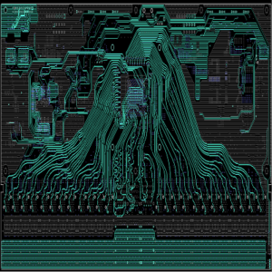
In PCB design, engineers often use via holes to connect the same electrical network located in different layers, vias and through holes PAD is very similar, the difference is that through holes pad is generally used to insert plug-in components, while via holes are generally small. Vias are very popular in some complex and multi-layer design, because it can serve as a pathway between the different layers.

What are vias in printed circuit boards (PCBs)?
Vias in printed circuit boards (PCBs) are essentially small holes that are drilled or etched into the board’s surface. These small, cylindrical holes are plated with conductive material, typically copper, to ensure electrical continuity between the layers. They serve as conduits for electrical connections between different layers of the PCB or between components mounted on the surface of the board and the internal circuitry.
They are important for creating multilayer PCBs, where multiple layers of copper traces are separated by insulating layers. Without vias, it would be impossible to establish connections between these layers, limiting the complexity and functionality of electronic devices.
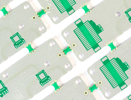
A via hole in PCB is mainly composed of three parts, hole, pads around the holes, and power layer isolation area. The process of via hole is to plate a layer of copper foil on the cylindrical surface of the hole wall by chemical deposition to connect the copper foil that needs to be connected in the middle of each layer. In this way, the upper and lower sides of the hole are made into ordinary pad shape, which can be directly connected with the traces of the upper and lower sides. The wall thickness of the plating is 1mil or 2mil, and completed hole diameter may be 2mil-4mil smaller than the drilled hole.
Why Employ Vias in PCBs?
Vias in PCBs primarily facilitate electrical connections across different board layers, enabling designers to craft intricate and compact circuit layouts by permitting signal and power traversal through layers. This capability is paramount in multi-layer PCBs, where space is constrained, and high-density component placement is requisite.
- Space Optimization
Vias permit the stacking of multiple circuit layers, optimizing PCB real estate, resulting in more compact devices.
- Enhanced Electrical Performance
Providing direct electrical signal pathways, reducing interference and loss, thereby enhancing overall circuit performance.
- Thermal Management
Thermal vias, specifically engineered for heat dissipation, aid in managing PCB temperatures, ensuring component reliability and longevity.
- Design Flexibility
Vias afford greater flexibility in routing traces and component placement, fostering more innovative and efficient PCB designs.
What are the different types of vias used in PCB design?
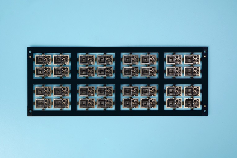
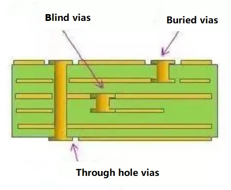
There are several types of vias, each serving different purposes based on their placement and function. Understanding the different types and their applications is crucial for designing efficient and reliable PCBs. The most common types include through-hole vias, blind vias, and buried vias. Each offers unique advantages depending on the design requirements and constraints of the PCB.
1. Through-Hole Vias: These are the most common type of vias, extending through the PCB’s entire thickness, linking all layers. They are straightforward to manufacture and cost-effective.
2. Blind Vias: These vias connect an outer layer of the PCB to one or more inner layers but do not go through the entire board. They conserve space and simplify board layout complexity.
3. Buried Vias: Located entirely within the inner layers of the PCB, buried vias connect two or more internal layers without reaching the outer surfaces. They are useful for high-density and multi-layer PCBs where space is limited.
4. Micro Vias: Smaller than standard vias, micro vias are typically utilized in high-density interconnect (HDI) PCBs. They can connect adjacent layers or span multiple layers using stacked or staggered configurations.
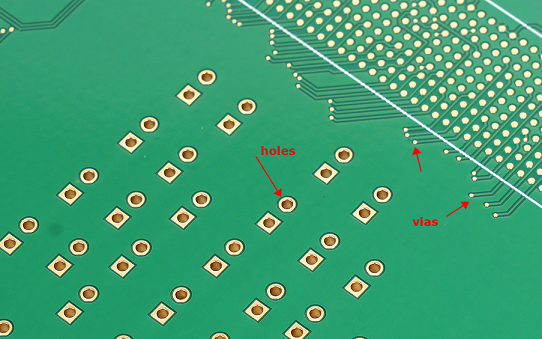
What is the difference between a PCB hole and a via?
The terms “PCB hole” and “via” are often used interchangeably, yet they denote distinct features within a PCB:
PCB hole generally refers to any drilled PCB hole, serving various purposes such as mounting components (e.g., plug-in components), positioning holes or mechanical mounting points. PCB holes are not necessarily conductive. While vias specifically denotes a conductive hole connecting different PCB layers. They are plated with conductive materials, usually copper, to ensure electrical continuity between layers.
In essence, while all vias are PCB holes, not all PCB holes are vias. Vias are a subset of PCB holes with the specific function of establishing electrical connections between layers, whereas PCB holes can serve a broader range of purposes, including mechanical and non-electrical functions.
What should we consider when designing vias in PCB?
In a PCB design, seemingly simple via holes often bring great negative effects to the design of the circuit. In order to reduce the adverse impact of the parasitic effect of the hole, PCB engineers can try their best to consider below points:
- Vias cannot be designed on the pads.
- The area extending 1.5mm outward from the contact region between the device’s metal housing and the PCB should not design any vias.
- Vias should not be present in the areas where adhesive dots are applied or printed for surface-mount components, such as the PCB areas beneath CHIP and SOP components when using adhesive dot application or printing processes.
- In principle, through-hole diameters should be at least 0.2mm (8mil) with an outer diameter of at least 0.4mm (16mil). For some special areas, the outer diameter must be controlled to 0.35mm (14mil).
- For BGA designs with a pitch of 0.65mm and above, it is advisable to avoid using blind or buried vias, as they significantly increase costs.
- The spacing between vias should not be too close to prevent drilling from causing breaks. Generally speaking, the hole spacing should be 0.5mm or more. Spacings of 0.35mm-0.4mm should be avoided as much as possible, and spacings of 0.3mm or less are prohibited.
- The number of vias used for power trace inter-layer connections should meet the current carrying requirements, which is 1A per 0.3mm diameter via.
This is the end of this informational sharing, welcome to contact us if you want to know more about PCBs.