Archive for October, 2022

How To Do Failure Analysis In Printed Circuit Board

Saturday, October 29th, 2022

Nowadays, printed circuit board plays a more and more important role in electronic products, whether for personal use or commercial use, failure PCB can effect the usage of electronic products and cause a serious consequence. So, how to quickly detect the PCB fault problem?

Here, Best Tech summarized seven methods to locate fault PCB quickly.

  • Use testing equipment

The typical equipment including Automated Optical Inspection (AOI) equipment, X-Ray Fluoroscopy, Optical Microscopy, 1000x magnifying glass. When some failures happen and we donā€™t know what is the specific position, properly use of these detection devices can help us quickly locate the faulty PCB.
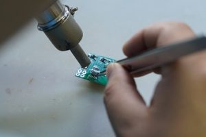
Scratch-on-PCB
  • Visual inspection

Visual inspection is the most common and easy method to position those defectives in printed circuit board. It can identify defects such as overlapped marks, solder joint short, signs of overheating circuit boards, and burned components.  When some problems are difficult to identify with our naked eye, magnifying glasses can help to identify some short circuits, welding bridges, open circuits, solder joints and circuit board wiring cracks, component offset, etc. 

  • Components inspection

If the printed circuit board was assembled with some electronic components, we can perform a components inspection to locate the failure. Especially when low resistance is detected between the component pins, it is best to remove the component from the PCB circuit for specialized testing. If the resistance is still low, then this component is the culprit, otherwise further investigation will be required.

  • Power on printed circuit board

Visual inspection is only suitable for checking the appearance of outer layers of the circuit board, instead of for checking the inner layer of the circuit board.  If there are no visible defects in the appearance, you can power up/on the board and perform a more detailed test to determine whether the board is working properly or not.

  • Low voltage measurement

The first thing to confirm is whether the voltage of each chip power pin is normal, and then check whether the various reference voltages are normal, and whether the working voltage of each point is normal. Since the copper trace on the circuit board has resistance, the voltage generated through different parts of the copper trace is also different.  Then you can use a voltmeter or multimeter to measure the voltage between different parts along a short. If you find that the voltage value is getting smaller and smaller, you are getting closer to find out a short circuit.

For a simple example, when a typical silicon triode is on, the BE junction voltage is around 0.7V, while the CE junction voltage is around 0.3V or less.  If the BE junction voltage of a triode is greater than 0.7V (except for special triode, such as the Darlington tube), the BE junction may be open.

  • Touch circuit board with your finger

In general, when some failure happened, some areas on the circuit board will be getting more and more heat. In this time, we can try to touch the circuit board with fingers to find out areas with heat, and it will help us to pinpoint the problem. However, be careful to use short-circuit copper trace power supply and avoid burns or electric shock.

  • Repair short/open

After identifying a short or open circuit on the PCB, the next step is to isolate the problem.  While this is easy to do on the outer surface of the board, it is a challenge for the inner layers.  Possible solutions include drilling through holes or cutting appropriate external copper traces.

This is the end of this article, if you have more better methods to locate the failure printed circuit board, warm welcome to contact us, we can analyze together.

You may also like

Why ENEPIG More Suitable for Ceramic PCB Wire Bonding?

Thursday, October 20th, 2022

There are many surface treatment choices that can be used on Ceramic PCB, but why ENEPIG is one of options we always recommend to our customers whom have wire bonding demands?

In the application of Ceramic PCB, COB or wire bonding was widely used for the packaging technology in thin, short, high speed of electronic products. The Chip On Board (COB) technology refers to a technology in which bare chips are directly attached to the PCB board and then connected electronically through metal wires, namely ā€œWire Bondingā€. Due to gold wire has an excellent electrical conductivity, thermal conductivity, corrosion and oxidation resistance, gold wire is often used as a main bonding material in microelectronics packaging.

What is ENEPIG?

ENEPIG, is a type of surface treatment on Printed Circuit Boards and ceramic PCB, the full name of it is Electroless Nickel ā€“ Electroless Palladium ā€“ Immersion Gold, now it is widely used in wire bonding field.

How does it work and what’s the standard thickness of each layer?

  • Electroless Nickel: Nickel acts as a barrier layer, preventing copper from interacting with the other metals involved in this plating technology, particularly gold. The layer is deposited on the catalytic copper surface using an oxidation-reduction reaction. The result is a layer that is between 2.0 to 5.0 microns thick.
  • Electroless Palladium: Palladium is a relatively stable metal at room temperature, and it is difficult to be oxidized within 400ā„ƒ. The chemically deposited palladium layer has a neat lattice arrangement, uniform grain size and compact structure. Adding palladium layer between nickel layer and gold layer can effectively prevent the diffusion of nickel layer to gold layer. The Palladium is a layer with a thickness between 0.03 to 0.10 microns, it also depends on the final applications.
  • Immersion Gold: The main function of the gold layer is to bond with the gold wire. If there is no palladium layer as a diffusion barrier between the nickel layer and the gold layer, the gold layer can also bond with the gold wire after reflow, as long as the gold layer reaches a certain thickness. For example, when the thickness of the electroplated nickel gold reaches 0.3um, it can bond with the gold wire. In addition, gold itself has a good bonding ability with gold wire, and in ENEPIG process, due to the palladium layer protects the gold layer from the pollution of nickel, only a thin gold layer (0.03um~0.05umm) is needed to have a good bonding property. Thisā€™s why thereā€™s cost advantage of ENEPIG than that of thicker ENIG.
(ENEPIG product)

Why choose ENEPIG?

ENIPIG has a good wiring bonding ability, solder joint reliability, multiple reflow soldering and excellent storage time, can correspond to and meet the requirements of a variety of different assemblies.Ā  Below is a comparison about performance of different surface treatments:

(Comparison-about-performance-of-different-surface-treatments)

AdvantagesĀ  of ENEPIG

  • ā€œBlack Nickelā€ free — The palladium layer separates the Nickel layer from the gold layer, it can prevents the mutual migration of gold and nickel, so no black nickel will appear
  • Excellent gold wire bondability — the gold plating/coating is very thin, can be used for gold wire bonding as well aluminum wire bonding
  • Palladium acts as an additional barrier layer to further reduce copper diffusion to surface, thus ensuring good solderability
  • Cost-effective than ENIG
  • Lead-free nickel
  • Good compatibility between coating and solder paste
  • Very suitable for packaging components such as SSOP, TSOP, QFP, TQFP, PBGA

Best Technology is a 16+ years PCB manufacturer and we made many ENEPIG PCBs and ceramic PCBs for our customers, welcome to contact us if you have demands on ENEPIG PCB.

You may also like

Why it is difficult to make different copper thicknesses on different layers for MCPCB

Friday, October 14th, 2022

With the development of technology, we need the MCPCB to be multi-layer. 1 layer MCPCB is not enough for making some high-quality precision equipment and products.

So now, 2 layers MCPCB becoming more and more popular.

Normally, we make 1OZ, 2OZ and 3OZ copper thickness for each layer for aluminum or copper core/base PCB. The thickness of copper for top and bottom layer are the same.

But recently, more and more customers want the MCPCB to be made with different copper thicknesses on top and bottom layer.

For example, they want 1OZ copper on top layer and 3OZ on bottom layer.

But we donā€™t suggest to do that, why? Let me do some explanations.

  1. Different copper thicknesses on top and bottom layer will increase the difficulty for production. Because we put the MCPCB into etching liquid to do the etching, we need to use film to protect one side from etching liquid, but if it canā€™t be protected well completely, it will be etching too, then it is rejected.
  2. Different copper thicknesses on different sided will cause the PCB twist finally if the stack up is double sided (See below double sided stack up)

But if the stack up is 2L (See below 2L stack up), the FR4 PCB is twisted then will affect the lamination for FR4 PCB and aluminum/copper base.

  1. Due to increase the difficulty of production, so the price will be increased too.
  2. Lead time will be longer than normal since the production process is much more completed.
  3. The reliability is not good.

Finally, it is better to do the same copper thickness for each layer for multi-layer MCPCB.

For knowing more knowledge about MCPCB, please email to sales8@bestpcbs.com

You may also like