pcb
Home > Blog

Archive for 7 月, 2023

Heavy Copper PCB for Industrial Power Supply
星期六, 29 7 月, 2023

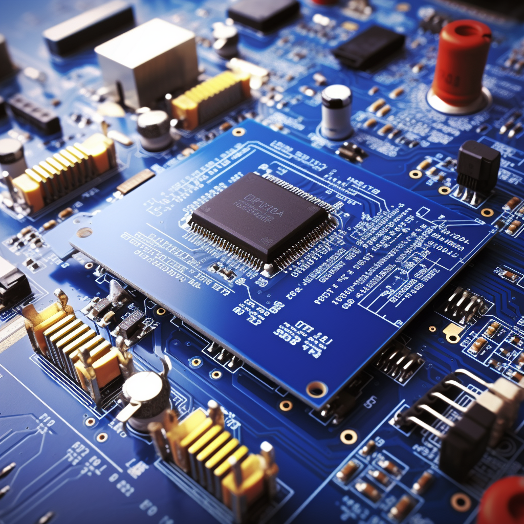
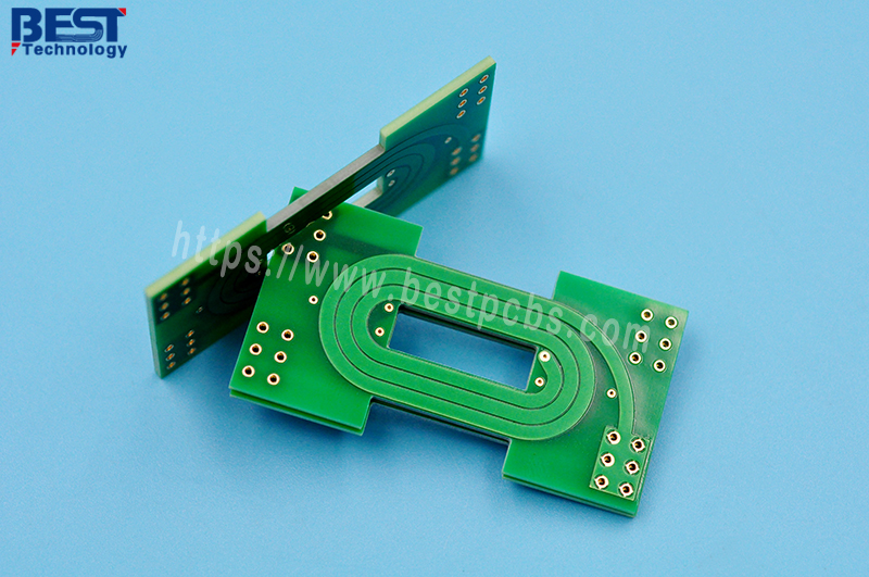
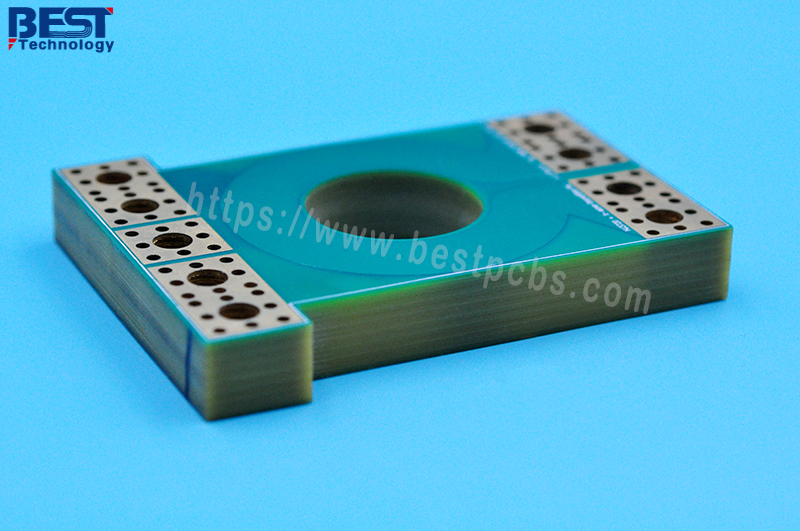
All of us know the printed circuit board, but do you know what is the heavy copper PCB? Best Tech is a very experienced heavy copper PCB fabricator since year 2006. Heavy Copper PCB is a type of printed circuit board that features with thicker copper layers than standard FR4 PCBs. While conventional PCBs typically have copper thicknesses ranging from 1 to 3 ounces (per square foot), heavy copper PCBs have copper thicknesses exceeding 3 ounces and can go up to 20 or more ounces. These copper layers are typically found in the inner and outer layers of the PCB, heavy copper providing enhanced current-carrying capacity and improved heat dissipation capabilities.

The increased copper thickness in heavy copper PCBs allows them to handle higher currents without experiencing excessive heat buildup or voltage drops. This makes them well-suited for applications that require high power handling, such as industrial power supplies, power converters, motor drives, and automotive electronics. Heavy copper PCBs are designed to withstand harsh operating conditions and provide robust performance and reliability.

Today, we would like to talk about the heavy copper PCB used in Industrial Power Supply. In this blog post, we will explore the realm of Industrial Power Supply, delving into the design considerations, material selection, production challenges, exceptional heat dissipation, and unrivaled conductivity of Heavy Copper PCBs. Join us on this enthralling journey as we uncover the secrets behind their application in Industrial Power Supply scenarios, including the testing of inductance, capacitance, and resistance. Get ready to witness the power of Heavy Copper PCBs in the realm of Industrial Power Supply!

Firstly, before you are moving start for the design, it need to get to understand the Design guideline rules of heavy copper PCB.

From the guidelines of heavy copper PCB, it could get to know it encompass considerations such as trace width, trace spacing, and thermal relief patterns. The increased copper thickness necessitates wider traces to accommodate higher currents, while proper spacing is crucial to avoid thermal hotspots and ensure reliable operation. Additionally, selecting suitable materials with excellent mechanical strength and thermal properties is vital to ensure the robustness and longevity of Heavy Copper PCBs. Hope this will bring some ideas to you during your design.

Secondly, as a heavy cooper PCB manufacturing vendor, Best Tech would like to advise the Production Challenges for the heavy copper PCB.

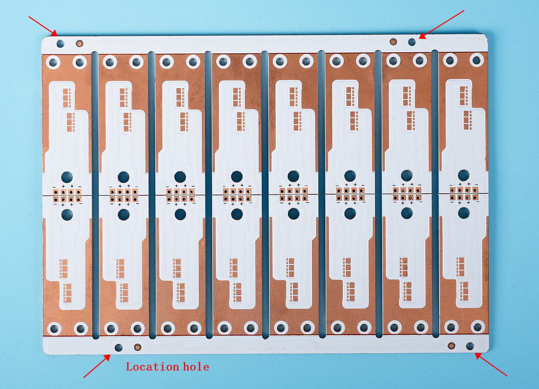
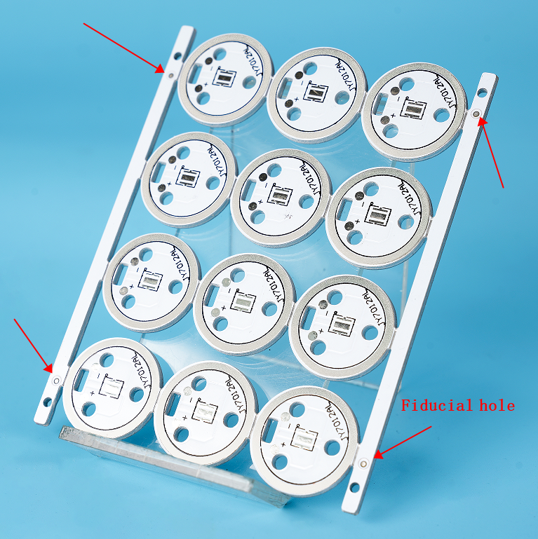
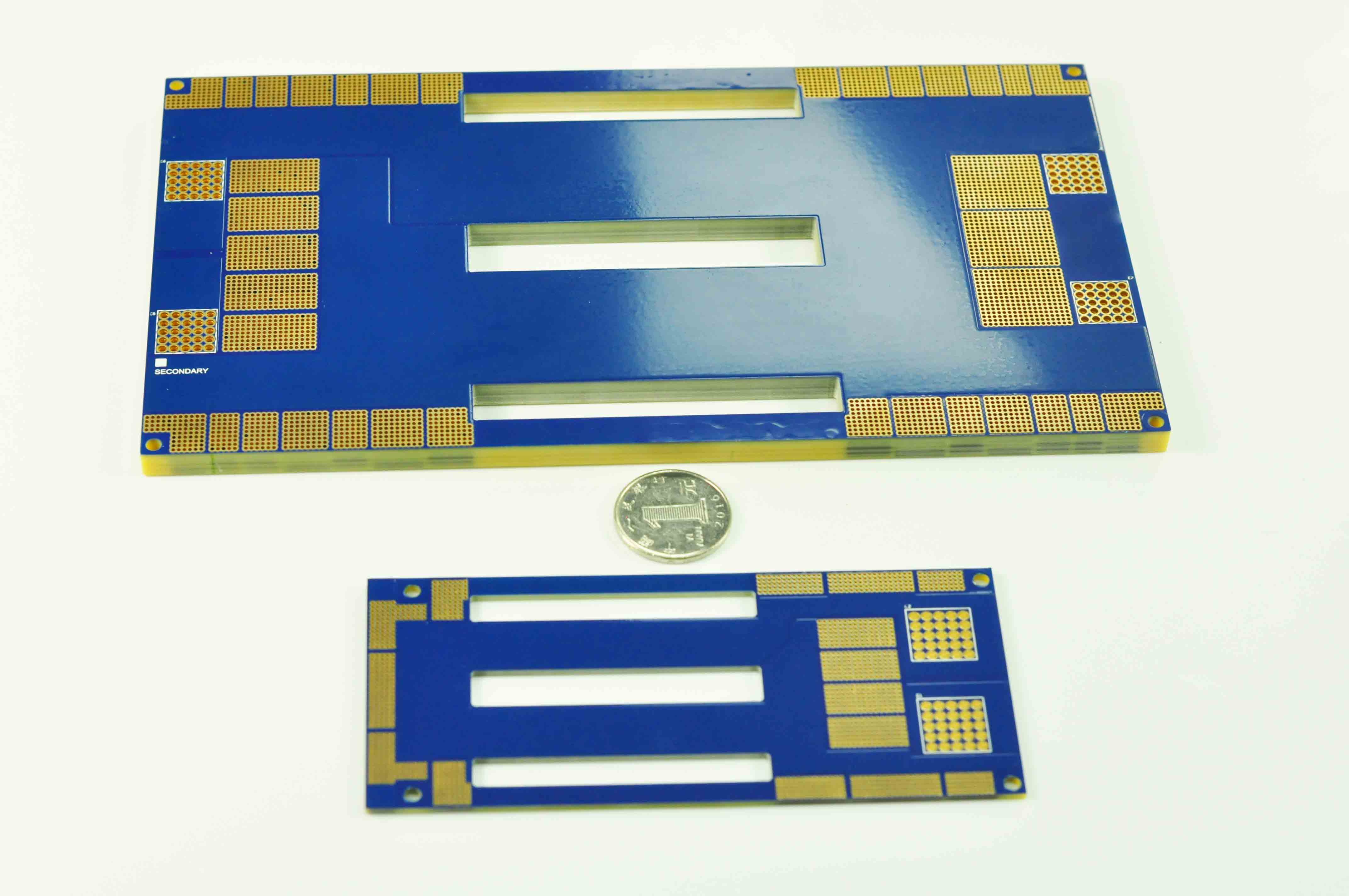
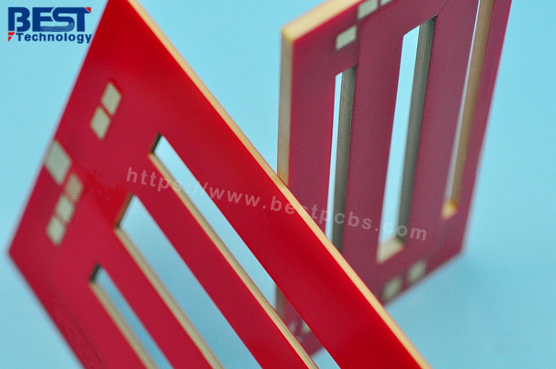
During producing Heavy Copper PCBs presents manufacturers with a set of intricate challenges. Achieving uniform copper thickness across the board’s surface demands advanced plating techniques and precise control over process parameters. Careful attention must be given to the etching process to prevent over-etching, which can compromise the integrity of the copper layers. Moreover, the additional weight of copper requires a sturdy substrate to support the board’s structure. Manufacturers must navigate these challenges with expertise and precision to deliver high-quality Heavy Copper PCBs.

You may have a question in mind, why we need to use the heavy copper PCB for the Industrial Power Supply, because the heavy copper PCB have Exceptional Heat Dissipation and Conductivity: One of the standout features of Heavy Copper PCBs is their unrivaled heat dissipation capabilities. The increased copper thickness acts as a robust conductor, efficiently channeling heat away from power components. This exceptional heat dissipation prevents thermal stress and ensures the longevity and reliability of Industrial Power Supply systems. Additionally, the high conductivity of Heavy Copper PCBs enables efficient power transmission, reducing losses and improving overall system efficiency.

Furthermore, Heavy Copper PCBs undergo rigorous testing to ensure optimal performance in Industrial Power Supply applications. Inductance testing verifies the effectiveness of copper layers in reducing magnetic interference. Capacitance testing evaluates the ability of the PCB to store electrical energy, while resistance testing determines the conductivity and resistance of copper traces. These tests play a crucial role in validating the quality and performance of Heavy Copper PCBs in demanding power supply scenarios.

Heavy Copper PCBs find widespread applications in the field of Industrial Power Supply, particularly in the production of robust and efficient power control products. They are integral components in industrial power converters, motor drives, uninterruptible power supplies (UPS), and various automation systems. The exceptional heat dissipation and high current-carrying capacity of Heavy Copper PCBs make them ideal for handling the power demands of these applications, ensuring reliable and efficient power delivery.

Finally, in the world of Industrial Power Supply, Heavy Copper PCBs emerge as true powerhouses, combining meticulous design, advanced manufacturing processes, and exceptional heat dissipation capabilities. By adhering to design guidelines, overcoming production challenges, and conducting thorough testing, Heavy Copper PCBs prove their mettle in demanding power supply scenarios. As they continue to evolve, these powerhouses will shape the future of Industrial Power Supply, empowering systems with reliability, efficiency, and unrivaled performance. Prepare to witness the electrifying impact of Heavy Copper PCBs in the realm of Industrial Power Supply!

If you have more question heavy copper PCB for Industrial Power Supply, warmly welcomed to contact Best Tech for more get more information of heavy copper PCB which used in Industrial Power Supply. You can visit www.bestpcbs.com to know more about us.

You may also like

Understanding Counterbore and Countersunk Holes in PCB Design
星期六, 8 7 月, 2023

When we talking about the holes in PCBs (Printed Circuit Boards), may somebody always curious about two special holes: Counterbore hole and Countersunk hole. They are easy to be confused and easy to misunderstanding if you are a layman of PCB. Today, we will introduce the differences between counterbore and countersunk for details, let’s keep reading!

What is a Counterbore Hole?

A counterbore hole is a cylindrical recess on a PCB that has a larger diameter at the top surface and a smaller diameter at the bottom. The purpose of a counterbore hole is to create space for a screw head or a bolt’s flange, allowing it to sit flush with or slightly below the PCB surface. The larger diameter at the top accommodates the head or flange, while the smaller diameter ensures that the fastener’s shaft or body fits snugly.

What is a Countersunk Hole?

On the other hand, a countersunk hole is a conical recess on a PCB that allows the head of a screw or bolt to sit flush with the PCB surface. The shape of a countersunk hole matches the profile of the fastener’s head, creating a seamless and level surface when the screw or bolt is fully inserted. Countersunk holes typically have an angled side, often 82 or 90 degrees, which determines the shape and size of the fastener head that will fit into the recess.

Counterbore VS Countersunk: Geometry

While both counterbore and countersunk holes serve the purpose of accommodating fasteners, their main difference lies in their geometry and the types of fasteners they accommodate.

Counterbore holes have a cylindrical recess with two different diameters, while countersunk holes have a conical recess with a single diameter.

Counterbore holes create a stepped or raised region on the PCB surface, whereas countersunk holes result in a flush or recessed surface.

Counterbore VS Countersunk: Fastener Types

Counterbore holes are primarily used for fasteners with a head or flange, such as bolts or screws that require a solid mounting surface.

Countersunk holes are designed for fasteners with a conical head, such as flathead screws or countersunk bolts, to achieve a flush surface.

Counterbore VS Countersunk: Drill angles

Different sizes and drilling angles of drill bits are offered for producing countersinks, depending on the intended use. These angles can include 120°, 110°, 100°, 90°, 82°, and 60°. However, the most frequently employed drilling angles for countersinking are 82° and 90°. For optimal outcomes, it is essential to align the countersink angle with the tapered angle on the underside of the fastener head. On the other hand, counterbore holes feature parallel sides and do not necessitate tapering.

Counterbore VS Countersunk: Applications

The choice between counterbore and countersunk holes depends on the specific requirements of the PCB design and the components being used.

Counterbore holes find applications in situations where a secure and flush fastening of components or mounting plates is necessary. They are commonly used to fasten connectors, brackets, or PCBs to an enclosure or chassis.

Countersunk holes are often employed when aesthetic considerations are important, as they provide a sleek and level surface. They are frequently used for mounting PCBs to surfaces where a flush finish is desired, such as in consumer electronics or decorative applications.

Counterbore and countersunk holes are important features in PCB design, enabling efficient component mounting and secure fastening. Understanding the differences between these two types of holes allows designers to select the appropriate option based on the specific requirements of their circuit board applications. Whether it’s ensuring a secure connection or achieving a visually pleasing finish, the choice between counterbore and countersunk holes plays a crucial role in the overall functionality and aesthetics of a PCB assembly.

You may also like

Do You Know How Many Types of Holes in PCB
星期二, 4 7 月, 2023

In the vast realm of engineering and manufacturing, there exists a hidden world of holes, each with its own distinct purpose and position. These holes play a crucial role in facilitating various functions within mechanical and electronic systems. In this blog, we will embark on a journey to explore different types of holes in printed circuit board. So, fasten your seatbelts and let’s delve into the fascinating world of these essential engineering features.

Common Types of Holes in PCB

Upon examining a circuit board, one will discover an array of holes serving specific purposes. These include Via holes, PTH, NPTH, Blind holes, Buried holes, Counterbore holes, Countersunk holes, Location holes, and Fiducial holes. Each hole type fulfills a distinct role and function within the PCB, making it crucial to familiarize oneself with their characteristics to facilitate optimal PCB design.

1. Via holes

Via holes are small openings that connect different layers of a printed circuit board (PCB). They facilitate the seamless flow of signals and power between the layers, enabling efficient circuit design and transmission. Vias can be classified into two types: Plated Through-Holes (PTH) and Non-Plated Through-Holes (NPTH), each serving different functions.

2. PTH (Plated Through-Hole)

Plated Through-Holes (PTH) are vias with conductive material coating the inner walls. PTHs establish electrical connections between different layers of a PCB, allowing the passage of signals and power. They play a crucial role in interconnecting components, facilitating the flow of electrical current, and ensuring the functionality of the circuit.

3. NPTH (Non-Plated Through-Hole)

Non-Plated Through-Holes (NPTH) lack the conductive coating on their inner walls, making them suitable for mechanical purposes only. These holes are used for mechanical support, alignment, or as positioning guides, without establishing any electrical connections. NPTHs provide stability and precision, ensuring proper alignment of components within the circuit board. The mainly different between PTH and NPTH is the copper foil will be plated in the hole wall while NPTH no need to do plate.

4. Blind Holes

Blind holes are partially drilled holes that penetrate only one side of a circuit board. They are primarily employed to connect the outer layer of the board with the inner layer, enabling component mounting on one side while remaining hidden from the other. Blind holes offer versatility and help maximize space in complex circuit board designs.

5. Buried Holes

Buried holes are entirely enclosed within a circuit board, connecting inner layers without extending to the outer layers. These holes are hidden from both sides of the board and serve to establish connections and routes between inner layers. Buried holes allow for denser circuit board designs, reducing the complexity of routing traces and enhancing the overall functionality of the board. They provide a seamless and compact solution without any surface exposure.

6. Counterbore Holes

Counterbore holes are cylindrical recesses created to accommodate the heads of bolts, nuts, or screws. They provide a flat-bottomed cavity that allows the fasteners to sit flush or slightly below the surface of the material. The primary function of counterbore holes is to enhance the aesthetics and functionality of a design by providing a smooth and even appearance. These holes are commonly found in woodworking, metalworking, and engineering applications where a concealed or larger bearing surface is desired.

7. Countersunk Holes

Countersunk holes are conical recesses designed to house the angled heads of screws or fasteners. They are employed to ensure that the screw heads lie flush or slightly below the material surface. Countersunk holes serve both aesthetic and practical purposes, providing a sleek and flawless finish while reducing the risk of snags or protrusions. Their versatility makes them suitable for various applications, from furniture manufacturing to aerospace engineering.

8. Location Holes

Location Holes, also known as Reference Holes or Tooling Holes, serve as key reference points for aligning and positioning components, parts, or fixtures during manufacturing or assembly processes. These holes are strategically placed in a design to ensure precise and consistent alignment, enabling efficient assembly and reducing errors.

9. Fiducial Holes

Fiducial Holes, also referred to as Fiducial Marks or Alignment Marks, are small precision holes or markings placed on a surface or PCB (Printed Circuit Board). These holes serve as visual reference points for vision systems, automated processes, or machine vision cameras.

As we conclude our journey through the fascinating world of holes in engineering, we have gained a deeper understanding of the functions and positions of counterbore holes, countersunk holes, via holes, PTH, NPTH, blind holes, and buried holes. These holes are essential elements in various industries, contributing to the aesthetics, functionality, and efficiency of designs.

After introducing each of them, you should have gained a deeper understanding of their functions, hope this is helpful for you the design holes on your PCB project!!

You may also like