Archive for April, 2021

What’s fiducial marks on the PCB?

Saturday, April 24th, 2021

You may ever be recommended by some PCB manufacturers to add the fiducial holes on the board edge. Do you know what is fiducial marks and what’s the purpose for this kind of holes in a PCB?

Now, let me to show you something for what is the fiducial holes.

Fiducial holes, we also call it fiducials mark, while we assemble a PCB, it will need to locate the positions for each component, and it is positioned based on the fiducial mark as the reference point.

There are 3 types fiducial marks, first type is fiducial marks on a single board, second type is the fiducial marks on a PCB panel, third one is the fiducial marks for some single component on the board.

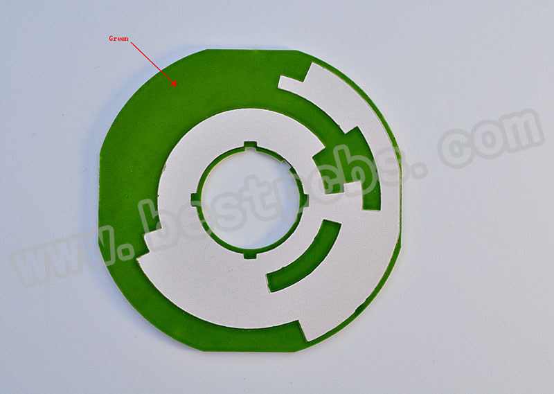
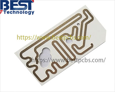
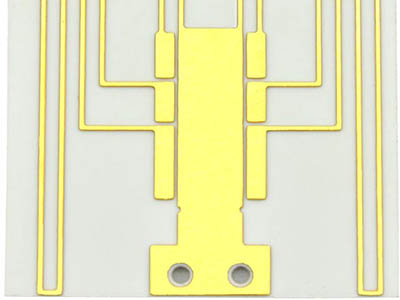
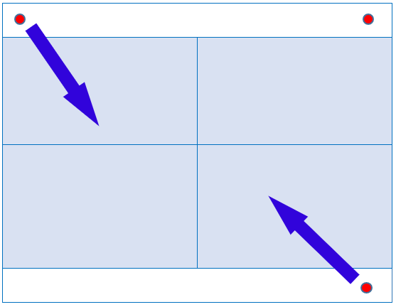
Here are the pictures for you to understand the types of the fiducials.

Fiducial holes types
Fiducial holes

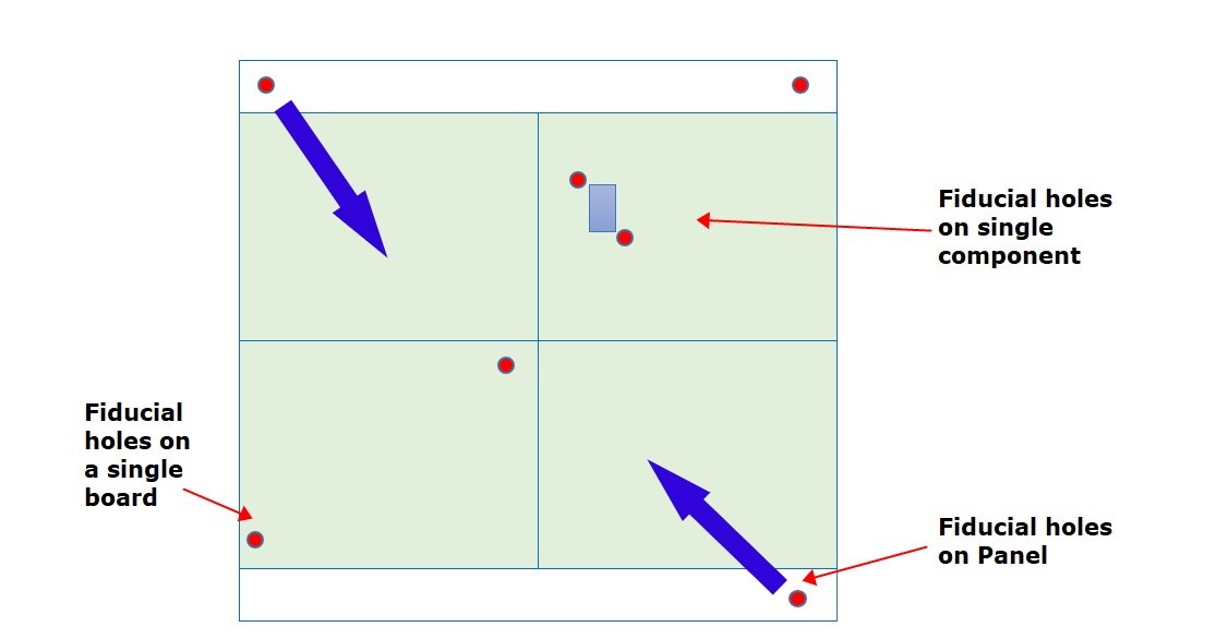
Fiducial mark on a single board is designed for positioned all circuits features on a single board. It is necessary to have a fiducial mark on a single board.

And fiducial marks on a PCB panel is used to assist positioning the circuits. 

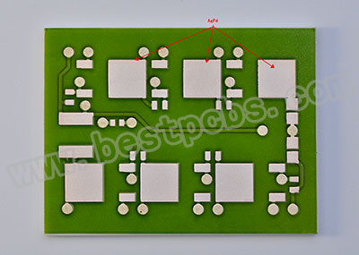
For the fiducial mark of a single component, it is designed to position the fiducial mark of a single component, which can improve the placement progress (For QFP, CSP, BGA and other important components must have the fiducial marks).

So, it is important to add the fiducial holes on a PCB board.

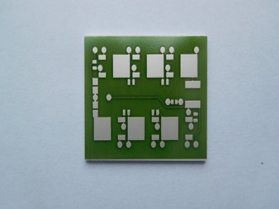
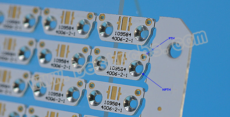
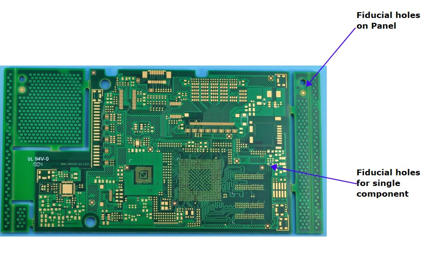
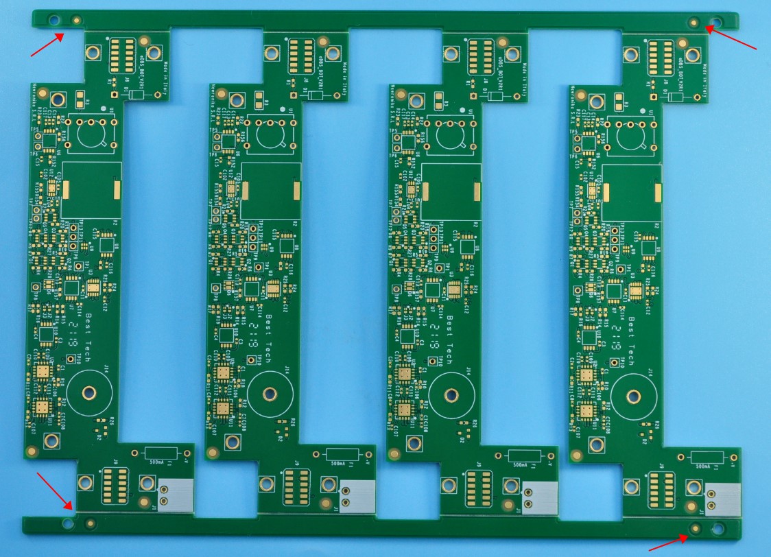
Also, while we make the panel for the PCB board, on the diagonal of the four corners, it is required to have 2 fiducial points at least on 2 diagonal corners.  you can also place 4 marks on the four corners, but generally, assembly plant will only need 2 marks for recognize.

See below a PCB panel for reference:

PCB panel drawing Best Technology
Fiducial holes on a panel

In the other hand, while you design the PCB, please try not to put the silk screens, pads, traces etc. within 2mm of the optical fiducial marks. Otherwise, the SMT machine will not be able to recognize the optical fiducial on the PCB boards.

And if you add the fiducial holes on the area which without any circuits, to avoid the holes being etching while the process, so generally we suggest to add a metal circles around the fiducial holes, to make it more obviously on the boards.

If you have any new PCB design which you also want to add the fiducial marks.

You are welcome to contact Best Technology for a help and we will show our best help for you.  

You may also like

What’s the differences between thick film ceramic PCB and DPC ceramic PCB

Wednesday, April 21st, 2021

Ceramic PCB including Alumina PCB (Al2O3 PCB), Aluminum Nitride PCB (AlN), Bryllium Oxide PCB(BeO PCB) etc.

There are other differences except the substrate material is different.

  1. The method of making conductor is different.

The conductor for thick film ceramic is made by printing, but DPC is made by vacuum sputtering and plating.

  • The conductor is different.

The conductor for thick film ceramic PCB is Au or AgPd, but for DPC ceramic PCB, it is copper.

  • The thickness of conductor is different.

Normally, it is 10-20um for thick film ceramic PCB, copper thickness can be 10um-300um for DPC ceramic PCB.

  • The solder mask is different.

It is glass glaze for thick film ceramic PCB, the most popular color is greenish and blue. Glass glaze can withstand very high temperature, up to 850C

It is normal solder mask oil for DPC ceramic PCB, the most popular color is white.

The above is only simple introduction for the difference, if you want to know more differences between thick film ceramic PCB and DPC ceramic PCB or other details about ceramic PCB, please contact us

You may also like

Why do MCPCB board have holes? What is PTH/NPTH

Thursday, April 15th, 2021

If you look closely at a MCPCB board, you will see holes of different sizes in the board, each hole was designed for a purpose. These holes can be divided into PTH (Plating Through holes) and NPTH (Non-Plating Through holes). Best Technology’s smallest drill tool is 0.5mm, so generally we require customers to design the minimum hole size of 0.5mm or more.

How to distinguish PTH and NPTH through holes?

In fact, it is very simple. Just look at the hole wall to see if there are bright plating traces (Copper). The holes with copper are PTH, and the holes without copper are NPTH.

PTH & NPTH

What is the NPTH used for?

If you pay a little attention, you will find that the size of NPTH is usually larger than the PTH, because most of NPTH are for positioning purposes, it can be divided into the following four types.

  1. 1) Countersink: It’s a cone-shaped hole that is cut into the PCB to allow the flat head of a socket cap screw to fit flush with the surface of the board.
  2. Counterbore: It’s a cylindrical flat-bottomed hole that is designed to house a hex head or socket head cap screw to be used to secure a PCB board.
Countersink & Counterbore
  • Screw hole: As shown as below.
As shown as below
  • Slot hole: Some components of the installation and positioning of the foot is rectangular or oval, we called this kind of irregular drilling as slot hole. During PCB machining, there are two types of drilling tools for plugins, one is called a drill cutter, which is used to drill round holes, and the other is called a routing bit, which is used to drill slot hole.
Slot hole

What is the PTH used for?

In order to connect the circuits between two or more layers, we need to design the PTH, which have following three main purposes.

  • Used for conducting electricity.
  • Used for heat dissipation.
  • Used for plug-in components.

If you have other questions about MCPCB, welcome to contact us

You may also like

What is Blind Via and Buried Via for Printed Circuit Board?

Thursday, April 15th, 2021

In the Printed Circuit Board industry, believe that you are familiar with blind via and buried via. What is blind via and buried via for PCB? And do you know is the Blind via or Buried Via have special application in your Printed Circuit Board?

In order to know more, we would like to share more information with you today.

Best Technology is an experienced FR4 PCB manufacturer in China since year 2006, with more than 15 years design and fabricate experience for PCB, Best Technology accumulated more than 1000 customers from all over the world.

Before start, we need to know what kinds of hole for FR4 Circuit Board, Via, Blind Via and Buried Via.

What is a Via?

Vias are the copper-plated holes in the PCB that allows the layers to layer connection. The standard via is called a through-hole via, but there are several disadvantages to using through-hole vias in Surface Mount Technology (SMT). For this reason, we often use a blind via or buried via instead. A blind or buried via can be processed in a wide range of different measures, including plugged copper mask via, a plugged solder mask via, plated via or staggered via.

Via
staggered via

What is Blind Via?

The via connects the external layer to one or more inner layers of the PCB and is responsible for the interconnection between that top layer and the inner layers.

Blind Via

What is Buried Via?

For a buried via, is the inner HOLE, between both sides in the board up and down inside the layer after pressing is cannot see. So, it doesn’t have to take up the outer area.

Buried Via

Blind and buried vias are particularly advantageous in HDI board because they optimize the density of the boards without increasing board size or the number of board layers you require. They are most commonly used in high-density PCB designs like, or in FPGA and custom chip packaging.Here is the photo which Best Technology took from our production line to make HDI Printed Circuit Board for our USA customer.

HDI board under production
HDI process

Best Technology is a very professional manufacturer in printed circuit board and HDI Board. If you are interesting to know more information of us, come to contact us and we are looking forward to discuss with you more for Printed Circuit Board.

You may also like