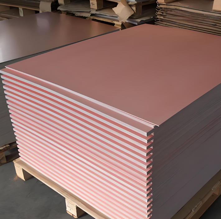
When searching for a reliable multi-layer PCB manufacturer, EBest is your first and best choice. We prioritize your project success with industry-leading delivery speed, uncompromising quality, authoritative certifications, free value-added services, and dedicated support—all designed to streamline your multi-layer PCB design, prototype, and production process.
- Delivery Speed: We offer fast turnaround times for both prototypes and mass production, ensuring your multi-layer PCB projects stay on schedule—no unnecessary delays, even for complex 4-16 layer designs.
- Unmatched Quality: Our multi-layer PCB production adheres to strict quality control standards, with precision layer alignment (±25μm tolerance), uniform copper etching, and bubble-free lamination to guarantee signal integrity and long-term reliability.
- Authoritative Certifications: EBest holds ISO 9001, IPC-6012, and RoHS certifications, ensuring our multi-layer PCB products meet global industry standards for automotive, medical, and industrial applications.
- Cost-Saving Support: We provide free DFM (Design for Manufacturability) analysis for all multi-layer PCB designs, helping you avoid costly reworks, and offer flexible prototype MOQ to support small-batch and startup projects.
- Dedicated Service: Our team of PCB engineers offers 24/7 technical support, guiding you through multi-layer PCB design, material selection, and production—ensuring your project runs smoothly from concept to delivery.
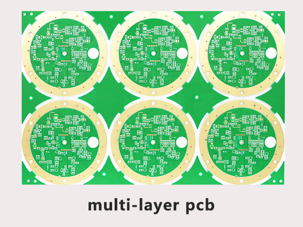
What is a Multi-layer PCB?
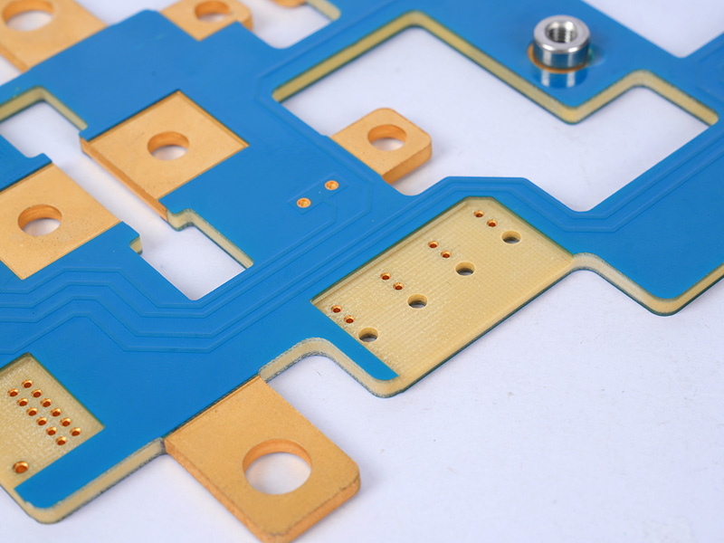
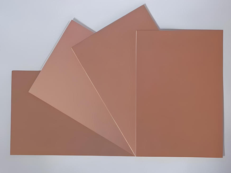
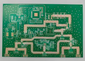
A multi-layer PCB is a printed circuit board composed of three or more conductive copper layers separated by insulating prepreg and core materials, bonded together through high-temperature and high-pressure lamination. Unlike single or double-layer PCBs, multi-layer PCBs use vias (through-holes, blind holes, buried holes) to connect layers, enabling higher component density, better signal integrity, and smaller board size—critical for modern electronic devices.

Most multi-layer PCBs range from 4 to 16 layers (high-layer PCBs have 20+ layers), with a typical thickness of 1.6mm for 4-layer designs. Their core advantage is balancing compactness with performance, making them ideal for devices requiring complex circuitry without sacrificing reliability.
Multi-layer PCB Stackup: A Complete Guide (Table Format)
The multi-layer PCB stackup design—the arrangement of copper layers, prepreg, and core materials—directly impacts signal integrity, power distribution, and thermal performance. Below is a detailed comparison of common stackup configurations for 4, 6, 8, and 10-layer PCBs, tailored to different application needs.
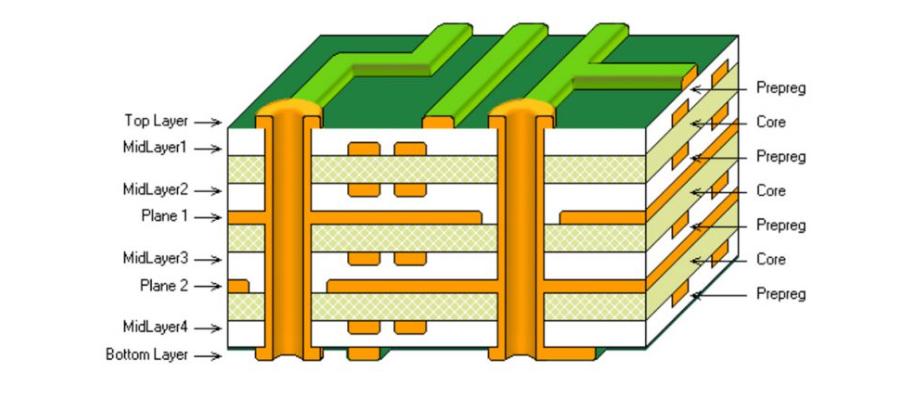
| Number of Layers | Stackup Configuration | Core/Prepreg Thickness | Copper Thickness | Key Application | Signal Integrity Focus |
|---|---|---|---|---|---|
| 4-Layer | Top (Signal) → Prepreg → GND → Core → POWER → Prepreg → Bottom (Signal) | Core: 0.8mm; Prepreg: 0.1mm | Outer: 1oz (35μm); Inner: 0.5oz (18μm) | Consumer Electronics, LED Lighting | Basic impedance control (50Ω) |
| 6-Layer | Top (Signal) → Prepreg → Signal → Prepreg → GND → Core → POWER → Prepreg → Signal → Prepreg → Bottom (Signal) | Core: 0.6mm; Prepreg: 0.1mm | Outer: 1oz; Inner: 0.5oz | Industrial Control, Power Electronics | Reduced crosstalk, improved power distribution |
| 8-Layer | Top (Signal) → Prepreg → Signal → Prepreg → GND → Prepreg → Signal → Core → Signal → Prepreg → GND → Prepreg → Bottom (Signal) | Core: 0.4mm; Prepreg: 0.08mm | Outer: 1oz; Inner: 0.5-1oz | Automotive Electronics, Communication Devices | Strict impedance control, EMC compliance |
| 10-Layer | Top (Signal) → Prepreg → Signal → Prepreg → GND → Prepreg → POWER → Core → POWER → Prepreg → GND → Prepreg → Signal → Prepreg → Bottom (Signal) | Core: 0.3mm; Prepreg: 0.08mm | Outer: 1oz; Inner: 1oz | Medical Electronics, Servers | High-speed signal integrity (DDR, PCIe), low noise |
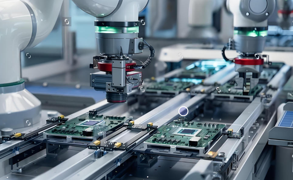
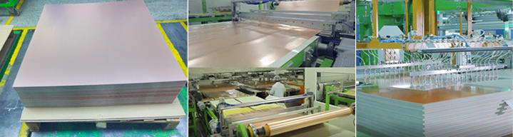
Multi-layer PCB Manufacturing Process: Step-by-Step
The multi-layer PCB manufacturing process requires precision and strict quality control to ensure layer alignment, conductivity, and reliability. Below is a detailed, step-by-step breakdown of the process, as executed by EBest’s expert team.
Step 1: Design Transfer & Panelization
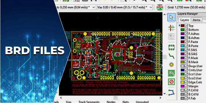
Start with a completed multi-layer PCB design (Gerber/ODB++ files) from your design software. We review the files for manufacturability, then combine individual PCB designs into a panel for efficient production. Fiducial marks and tooling holes are added to ensure precise alignment in subsequent steps.
Step 2: Inner Layer Processing
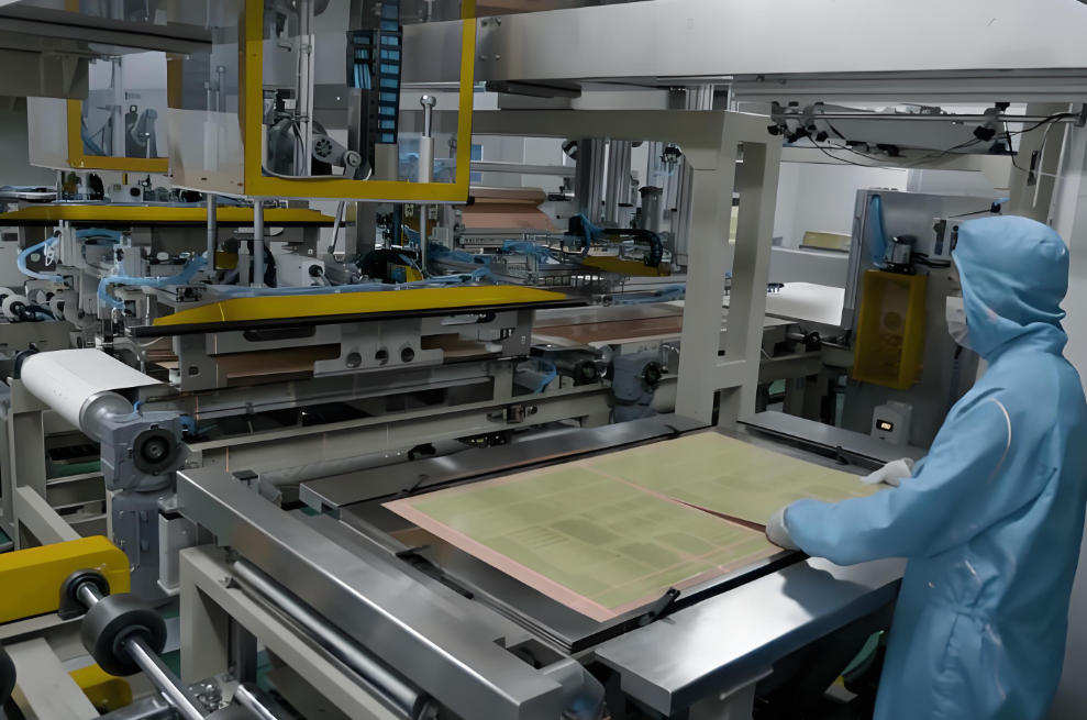
Cut copper-clad laminate sheets to size, clean the copper surfaces, and apply a photosensitive photoresist. Expose the inner layers to UV light through a photomask to transfer the circuit pattern, then develop and etch the layers to remove unwanted copper. Each inner layer is inspected for defects using AOI (Automated Optical Inspection).
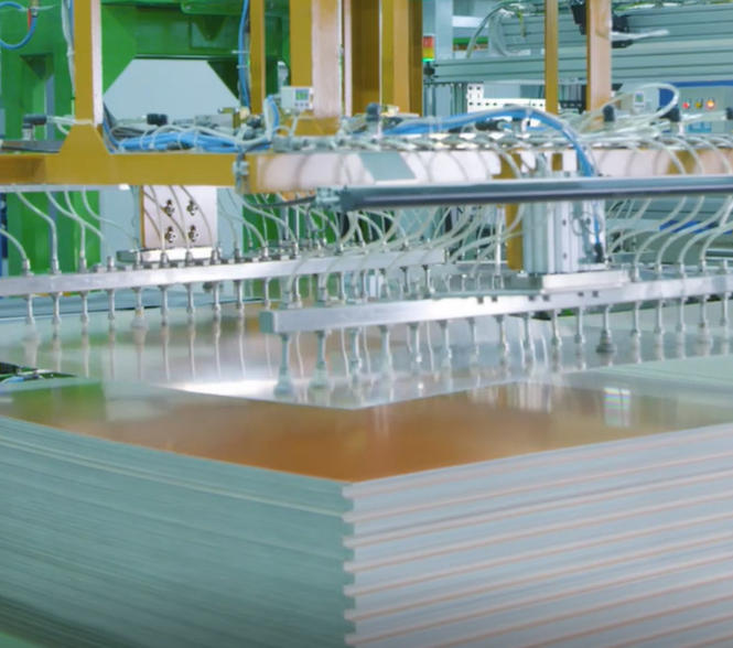
Step 3: Layer Stackup & Lamination
Stack the inner layers, prepreg, and outer copper-clad laminates according to the predetermined multi-layer PCB stackup design. The stack is placed in a lamination press, where heat (up to 180°C) and pressure (≥6kg/cm²) bond the layers together, melting the prepreg to form a solid board. We use low-flow prepreg to prevent layer shifting and bubble formation.
Step 4: Drilling
Use computer-controlled drilling machines to create vias (through-holes, blind holes, buried holes) for layer interconnection. For high-aspect-ratio holes (up to 8:1 in 8-layer PCBs), we use step drills to prevent breakage. The drilled board is cleaned to remove debris and residues.
Step 5: Plating
Electroplating is used to coat the hole walls and copper traces, ensuring electrical conductivity. We use pulse plating to achieve uniform copper thickness (20-35μm) and improve hole wall quality. A final copper plating layer is applied to meet the required thickness for signal and power layers.
Step 6: Outer Layer Processing & Solder Mask Application
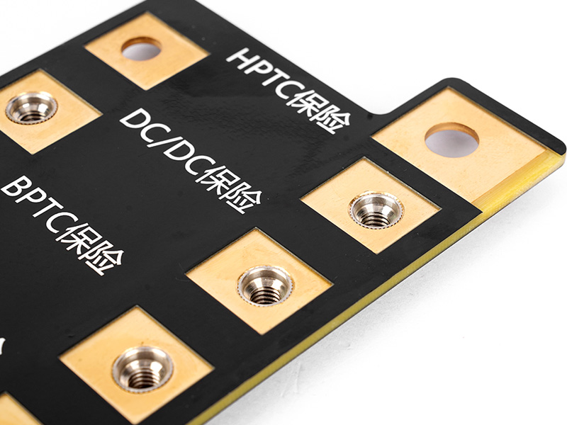
Repeat the photoresist, exposure, and etching process for the outer layers to form the final circuit pattern. A solder mask (green, black, or custom color) is applied to protect the copper traces from oxidation and short circuits. Silkscreen printing adds component labels for assembly.
Step 7: Surface Finish & Final Inspection
Apply the appropriate surface finish (ENIG, HASL, OSP) based on your application. We perform final inspections, including AOI, X-ray (for inner layer defects), and electrical testing (continuity, insulation resistance) to ensure the multi-layer PCB meets all specifications.
Multi-layer PCB Design Guide: Solve Pain Points & Optimize Performance
Designing a multi-layer PCB comes with unique challenges that can derail projects if not addressed properly. Below are the most common design pain points, their impacts, and EBest’s proven solutions—plus why you should trust us for your multi-layer PCB design needs.
Common Multi-layer PCB Design Pain Points & EBest’s Solutions
- Pain Point 1: Signal Integrity Issues (Crosstalk, Reflection, Delay)
High-speed signals (≥100MHz) on multi-layer PCBs often suffer from crosstalk, reflection, or delay, leading to signal distortion and circuit failure. This is especially common in dense designs with closely spaced traces.
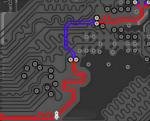
Solution: EBest’s engineers optimize your multi-layer PCB signal integrity optimization by placing signal layers adjacent to ground planes, using differential pair routing (equal length, 3x line width spacing), and adding appropriate termination resistors (50Ω/75Ω). We also use 3D electromagnetic simulation to predict and resolve signal integrity issues before production.
- Pain Point 2: Power Integrity Problems (Voltage Noise, Fluctuations)
Voltage noise and fluctuations on power planes can cause chips to reset or malfunction, especially in multi-layer PCBs with multiple power domains.
Solution: We design multi-layer PCBs with adjacent power and ground planes to form a natural capacitor, reducing noise. We also place decoupling capacitors (0.1μF + 10nF) near chip power pins and split power planes (with proper isolation) for different voltage domains.
- Pain Point 3: Layer Alignment Errors
Poor layer alignment (beyond ±25μm) causes via misalignment, short circuits, or open circuits—especially in 8+ layer multi-layer PCBs.
Solution: EBest uses precision alignment tools during lamination and adds fiducial marks to every panel. We also implement thermal expansion compensation to minimize alignment errors caused by material temperature changes.
- Pain Point 4: Heat Dissipation Challenges (Overheating Components)
High-power components on multi-layer PCBs can overheat, reducing component lifespan and performance—critical in automotive and industrial applications.
Solution: We integrate heat dissipation vias, large copper heat dissipation pads, and (if needed) metal core layers into your multi-layer PCB design. We also optimize component placement to avoid heat concentration and ensure airflow.
Don’t let multi-layer PCB design challenges slow down your project. EBest’s team of design engineers will guide you from concept to final design, ensuring your multi-layer PCB is optimized for performance, manufacturability, and reliability. Choose EBest for your multi-layer PCB design needs—we turn complex designs into actionable solutions.
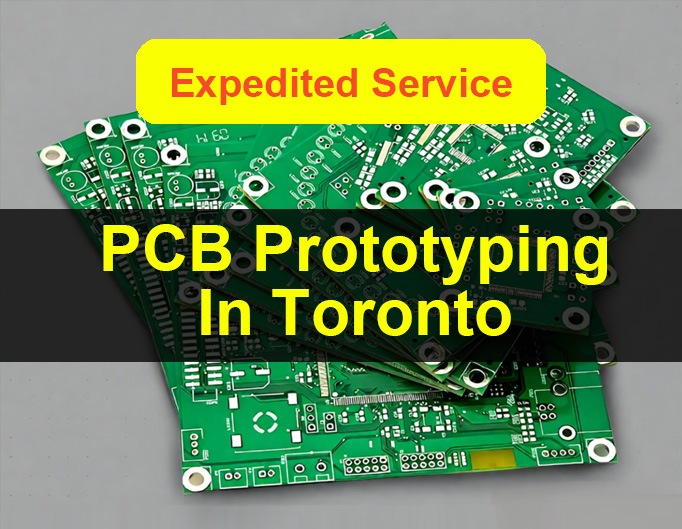
High-Precision Multi-layer PCB Prototype: Fast, Reliable, and Customizable
A high-quality high-precision multi-layer PCB prototype is critical to validating your design, identifying issues early, and accelerating time-to-market. However, many engineers face frustrating pain points when sourcing multi-layer PCB prototypes—here’s how EBest solves them, and why you should choose us for your prototype needs.
Common Multi-layer PCB Prototype Pain Points & EBest’s Solutions
- Pain Point 1: Slow Turnaround Times
Many manufacturers take 7-10 days to deliver high-precision multi-layer PCB prototype, delaying design validation and project timelines.
Solution: EBest offers fast prototype turnaround—48-72 hours for 4-6 layer multi-layer PCB prototypes, and 5-7 days for 8-10 layer designs. We prioritize prototype orders to ensure you get your boards quickly.
- Pain Point 2: Poor Prototype Quality (Misalignment, Defects)
Low-quality multi-layer PCB prototypes (with layer misalignment, etch errors, or poor soldering) lead to incorrect design validation and costly reworks.
Solution: EBest applies the same strict quality control standards to prototypes as mass production. We use LDI (Laser Direct Imaging) for precise circuit patterns, AOI inspection, and X-ray testing to ensure your high-precision multi-layer PCB prototype is defect-free.
- Pain Point 3: Inflexible Customization
Many manufacturers limit customization options for multi-layer PCB prototypes, making it hard to test unique design requirements (e.g., high-frequency materials, custom stackups).
Solution: EBest offers fully customizable high-precision multi-layer PCB prototype—choose layer count (4-16 layers), materials (FR-4, PTFE, high-TG), surface finish, and thickness. We also provide free DFM analysis to ensure your custom prototype is manufacturable.
- Pain Point 4: Lack of Technical Support
When issues arise with your multi-layer PCB prototype, many manufacturers offer little to no technical support, leaving you stuck.
Solution: EBest’s engineers are available 24/7 to answer your multi-layer PCB prototype questions, help troubleshoot design issues, and provide guidance on optimizing your prototype for mass production.
For high-precision, fast, and reliable high-precision multi-layer PCB prototype, choose EBest. Our prototypes are built to the same standards as production boards, ensuring accurate design validation and a smooth transition to mass production. Contact us today to start your multi-layer PCB prototype project.
How to Choose Multi-layer PCB Raw Materials? (Table Comparison)
The choice of raw materials directly impacts the performance, reliability, and cost of your multi-layer PCB. Below is a detailed comparison of common multi-layer PCB material selection, their properties, and ideal applications—helping you make the right choice for your project.
| Material Type | Dielectric Constant (Dk) | Loss Factor (Df) | Thermal Conductivity | Key Properties | Ideal Application |
|---|---|---|---|---|---|
| FR-4 (Standard) | 4.2-4.8 (1GHz) | 0.020-0.025 | 0.3 W/mK | Cost-effective, good mechanical strength, widely available | Consumer Electronics, LED Lighting, Basic Industrial Control |
| FR-4 (High-TG) | 4.0-4.5 (1GHz) | 0.018-0.022 | 0.35 W/mK | High heat resistance (TG >180°C), improved reliability | Automotive Electronics, Servers, Industrial Control |
| PTFE (High-Frequency) | 2.2-3.5 (1GHz) | <0.004 | 0.6-1.2 W/mK | Low loss, excellent high-frequency performance | Communication Devices (5G), Aerospace, Radar |
| Metal Core (Aluminum/Copper) | 4.5-5.0 (1GHz) | 0.030-0.050 | 1-10 W/mK | High thermal conductivity, good heat dissipation | Power Electronics, LED Lighting, High-Power Industrial Devices |
| Copper Foil (ED) | N/A | N/A | 401 W/mK | Cost-effective, rough surface (good adhesion) | Inner Layers of Standard Multi-layer PCBs |
| Copper Foil (RA) | N/A | N/A | 401 W/mK | Smooth surface, low high-frequency loss | High-Speed Multi-layer PCBs (DDR, PCIe) |
EBest’s engineers will help you select the optimal multi-layer PCB material selection for your multi-layer PCB, based on your application, performance requirements, and design constraints. We source high-quality materials from trusted suppliers to ensure consistent quality across all your multi-layer PCB projects.
Multi-layer PCB Applications: Industry Use Cases & Common Issues
Multi-layer PCBs are essential in modern electronic devices, especially in industries requiring compact, high-performance, and reliable circuitry. Below are four popular industries for multi-layer PCBs, real-world case studies, and common application issues with solutions.
1. Consumer Electronics
Case Study: EBest designed and manufactured 4-layer multi-layer PCBs for a smartwatch brand. The PCBs needed to be compact (30x30mm) with high component density, supporting Bluetooth, heart rate monitoring, and battery management.
Common Issue: Signal interference between Bluetooth and heart rate sensor circuits. Solution: We used a 4-layer stackup with separate signal and ground layers, optimized trace routing, and added shielding to minimize interference. The final multi-layer PCBs met all performance requirements and passed FCC testing.
2. Automotive Electronics
Case Study: EBest supplied 8-layer automotive multi-layer PCB manufacturing for an electric vehicle (EV) battery management system (BMS). The PCBs needed to withstand high temperatures (-40°C to 125°C) and support high-current (20A) power distribution.
Common Issue: Thermal degradation and voltage noise. Solution: We used high-TG FR-4 material, integrated heat dissipation vias and large copper pads, and designed adjacent power/ground planes to reduce noise. The automotive multi-layer PCB manufacturing passed automotive qualification (AEC-Q200) and are now in mass production.
3. Medical Electronics
Case Study: EBest developed 10-layer medical multi-layer PCB solutions for a portable ultrasound device. The PCBs needed to support high-speed data transfer (1Gbps) and meet strict medical standards (ISO 13485).
Common Issue: Signal integrity and biocompatibility. Solution: We used low-Df materials, differential pair routing for high-speed signals, and ENIG surface finish (biocompatible). The medical multi-layer PCB solutions met all medical certifications and enabled the device to deliver clear ultrasound images.
4. Industrial Control
Case Study: EBest manufactured 6-layer multi-layer PCBs for a programmable logic controller (PLC). The PCBs needed to resist electromagnetic interference (EMI) and support multiple I/O channels.
Common Issue: EMI interference from industrial equipment. Solution: We designed a 6-layer stackup with full ground planes for shielding, added EMI filters to input/output ports, and optimized trace spacing. The multi-layer PCBs operate reliably in harsh industrial environments.
What Are the Most Common Multi-layer PCB Problems?
Even with careful design and manufacturing, multi-layer PCBs can face common issues that impact performance. Below are the most frequent problems, their causes, and quick solutions—helping you avoid costly reworks and delays.
- Issue: Layer Delamination
Cause: Poor lamination (insufficient heat/pressure), low-quality prepreg, or moisture in materials. Solution: Use high-quality prepreg, ensure proper lamination parameters, and store materials in a dry environment. EBest uses vacuum lamination to prevent delamination.
- Issue: Via Open Circuits
Cause: Drilling errors, poor plating, or debris in holes. Solution: Use precision drilling machines, clean holes thoroughly before plating, and perform electrical testing. EBest uses X-ray testing to detect via defects early.
- Issue: Impedance Mismatch
Cause: Incorrect trace width, spacing, or material Dk. Solution: Calculate trace dimensions based on impedance requirements, use consistent materials, and simulate impedance before production. EBest’s DFM service includes impedance checking.
- Issue: Copper Etching Errors
Cause: Over-etching/under-etching, poor photomask alignment. Solution: Use LDI for precise photomask alignment, control etching time/temperature, and perform AOI inspection. EBest uses automated etching equipment for consistent results.
Multi-layer PCB FAQ: Answers to Common Questions
Below are the most frequently asked questions about multi-layer PCBs, with clear, concise answers—designed to address your most pressing concerns and help you make informed decisions.
1. What is the maximum number of layers for a multi-layer PCB?
EBest can manufacture multi-layer PCBs with up to 24 layers, though the most common range is 4-16 layers. The maximum layer count depends on your design requirements (component density, signal speed) and application. High-layer multi-layer PCBs (20+ layers) are typically used in aerospace and high-end server applications.
2. How long does it take to manufacture a multi-layer PCB?
Turnaround time varies by layer count: 4-6 layer multi-layer PCBs take 5-7 days for mass production, 8-10 layer PCBs take 7-10 days, and 12+ layer PCBs take 10-14 days. Prototypes are faster—48-72 hours for 4-6 layers and 5-7 days for 8+ layers.
3. Can multi-layer PCBs be used for high-frequency applications?
Yes, multi-layer PCBs are ideal for high-frequency applications (≥1GHz) when using low-Df materials (e.g., PTFE, hydrocarbon resin) and optimized stackup. EBest designs high-frequency multi-layer PCBs with controlled impedance, minimal crosstalk, and low signal loss for 5G, radar, and satellite communication devices.
4. How to test the quality of a multi-layer PCB?
Quality testing for multi-layer PCBs includes AOI (for surface defects), X-ray (for inner layer defects and via alignment), electrical testing (continuity, insulation resistance, impedance), and thermal testing (for heat resistance). EBest performs 100% testing on all multi-layer PCBs to ensure compliance with industry standards.
5. What is the difference between blind holes and buried holes in multi-layer PCBs?
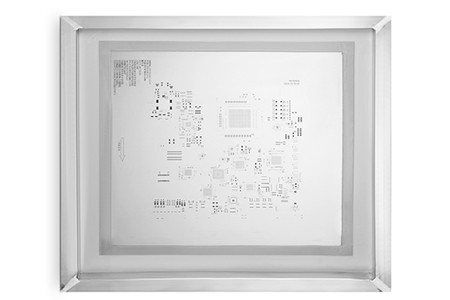
Blind holes connect the outer layer to one or more inner layers (but not all layers), while buried holes connect two or more inner layers (not the outer layers). Both are used in multi-layer PCBs to save space and improve signal integrity, especially in dense designs. EBest can manufacture both blind and buried holes with high precision.
6. Are multi-layer PCBs more reliable than single/double-layer PCBs?
Yes, multi-layer PCBs are more reliable than single/double-layer PCBs for complex applications. They offer better signal integrity, reduced crosstalk, improved power distribution, and higher component density—all of which reduce the risk of circuit failure. They also withstand harsh environments (temperature, humidity, EMI) better than single/double-layer PCBs.
7. How to reduce crosstalk in multi-layer PCB designs?
To reduce crosstalk in multi-layer PCBs, place signal layers adjacent to ground planes, use differential pair routing (equal length, 3x line width spacing), minimize parallel trace length, and increase trace spacing. EBest’s design team uses these techniques and 3D simulation to minimize crosstalk in all multi-layer PCB signal integrity optimization designs.
Choose EBest for Your Multi-layer PCB Needs
At EBest, we specialize in multi-layer PCB design, prototype, and manufacturing—delivering high-quality, reliable, and cost-effective solutions for consumer electronics, automotive, medical, and industrial applications. Our team of expert engineers is dedicated to solving your multi-layer PCB challenges, from design to delivery, and our strict quality control ensures every board meets your specifications.
We provide multi-layer PCB products with fast delivery, free DFM analysis, flexible customization, and 24/7 technical support. Whether you need a high-precision prototype or mass production, EBest is your trusted partner for all multi-layer PCB needs. Contact us today to place your order—send an email to sales@bestpcbs.com and let’s bring your project to life.