It is widely known that BeO with high thermal conductivity (200-250W/m.k).
High dielectric constant 6-7 (0.1MHz) and dielectric loss tangent is 10-4 (0.1GHz).
It is ideal material for ceramic PCB, lots of engineers want to use it as DBC ceramic PCB substrate.
But it is unfeasible, the powder of BeO is extremely poisonous.
The poison gas is produced by the reaction between oxygen, Cu and BeO under
1065-1085 degrees Celsius, so it is limited to make cooper on BeO substrate,
it has caused AlN (Aluminium Nitride) is becoming more and more popular.
Though BeO is unfeasible for DBC technology, but it is feasible for thick film technology.
Because when doing the conductor (Au or AgPd) on BeO substrate, we use silk-screen printing, no need to under high temperature environment, there is no chemical reactions.
Below the manufacturing process for your reference.
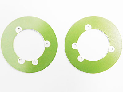
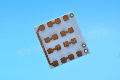
Here is the photo of BeO with AgPd conductor.