Archive for July, 2020

How to avoid circuits issue while the production process ?

Monday, July 13th, 2020

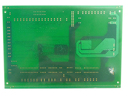
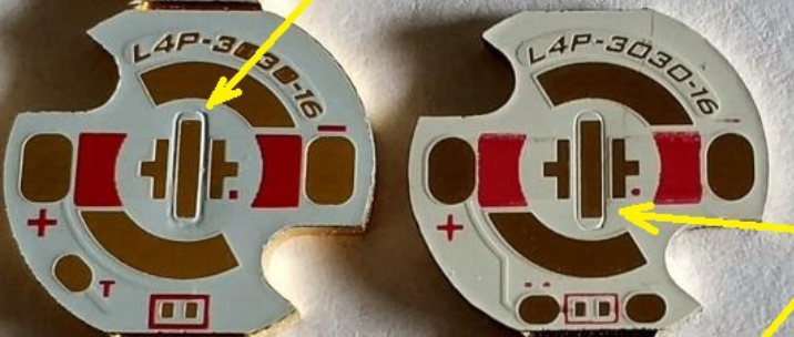
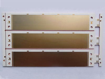
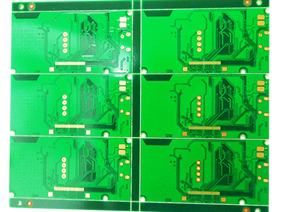
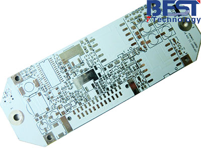
As we all know, the short & open circuits is a very common issues for the Printed Circuits Board, especially for the extra thin PCB, because its substrates thickness are very thin, generally from 0.4mm-0.15mm, so the circuits will be easy to be broken if we didn’t control the production process well.

So, you may want to know, as an experienced PCB manufacturer, what we will do to avoid the circuits issues?

Here let me show you what we do:

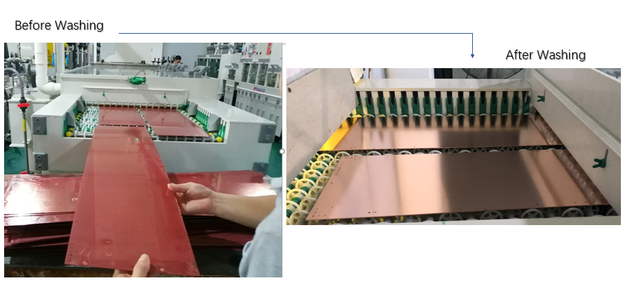
Firstly, after the process of copper plating, we will put the boards into our washing line to remove those drilling burr, surface oxide layer, etc.  To make sure the boards are fully clean before start the traces making process.

pcb washing
pcb washing

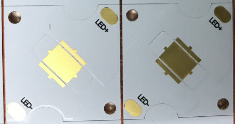
Actually, most of the open and short circuits problem are caused by the film scratching, so each operation while the pattern transfer process is very important.

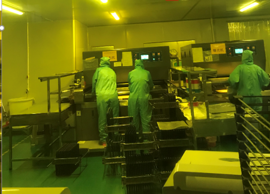
That’s also why the exposure and developing need to be processed in the dust-free workshop. We will use the rack to place each PCB board separately, to avoid the touching between PCB.

pcb explosure and developing

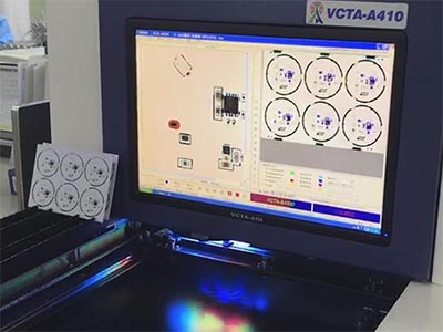
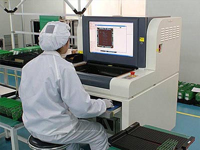
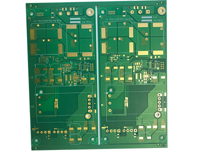
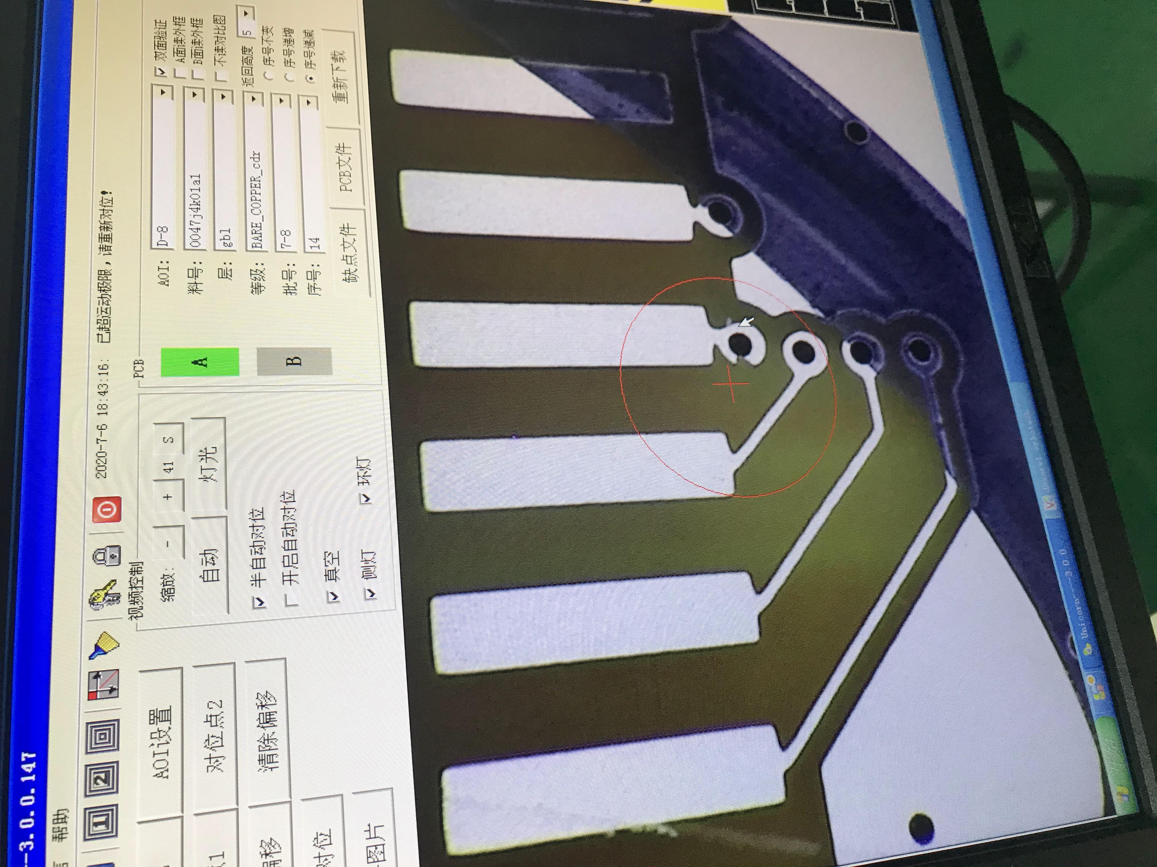
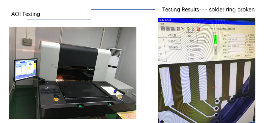
After the circuits etching out, we will take the boards to do the AOI testing, to check if there are any broken circuits, short gaps, protrusions, copper surface garbage and other problems. If there is, our machine will alert the problem, and we will fix the problem or scrap the defectives boards, with this process to prevent the defective boards move to the next step.

Most importantly is that we will do the first article inspection for all the boards, as long as we found the circuits issues while the AOI process, we will not take the whole batch boards go ahead.

aoi testing
aoi testing

Besides, the operation standard while the etching process is also very important for how the traces being. So, our production team will control the running speed of the etching machine very strictly. If it is a PCB with o.5oz bottom copper , only allow walk 1.4 meters at per minute, if 2oz, walk 0.8m one minute.

etching pcb
etching pcb

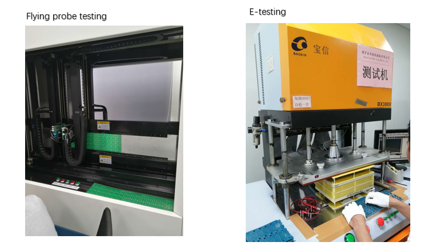
Except above process, all the boards will be required to do a final electrical testing before move to the packing. For prototypes, we will use flying probe testing. For volume, we will open the E-testing fixture to do the testing.

In our company, for the extra thin PCB, if the boards thickness lower than 0.2mm to do the flying probe testing, it needs to be tested before the outline process, because the boards are too thin to support the boards well while the flying probe, it will fall down easily.

flying probe testing and electric testing

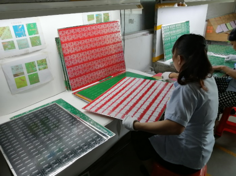
Of course, our QC people will do the double visual inspection to make sure all the boards are being well made.

fr4 pcb inspection
fr4 pcb inspection

We always try our best effort to prevent any defective boards send to customers.  

Quality and Customers Scarification, it is always our company’s pursuit.

You may also like

How to improve the gap between the convexity and LED pad?

Saturday, July 11th, 2020

About the SinkPad copper core PCB, all is known that convexity is very important, the height of convexity is about 0.2mm-0.25mm.

We need to know what’s the reasons caused the gap between the convexity and LED pad is big.

  1. We make the copper core with convexity firstly, then make the circuit/panel board (FR4PCB/BT PCB) and finally do the lamination for cooper core and circuit board.
  2. The tolerance for convexity is +/-0.05mm-0.075mm.
  3. The tolerance for circuit/panel board is +/-0.13mm.

If we do negative tolerance for convexity and positive tolerance for circuit/panel board, then it will cause the gap very big.

See below picture and details.

For example, the size of convexity is 0.5mm, after negative tolerance -0.075mm, it will be 0.425mm and each side will be 0.0375mm smaller.

For the circuit/panel board, the gap between convexity is 0.2mm, after positive tolerance +0.13mm, it will be 0.33mm and each side will be 0.065mm bigger.

So finally, the gap will be 0.2mm+0.0375+0.065mm=0.3025mm. It is about 50% bigger than original size.

sinkpad pcb
sinkpad pcb
sinkpad pcb
Big gap between convexity and LED pad

How to improve that problem?

  1. Making the copper core with convexity according to design.
  2. Measuring the dimension of convexity before making the circuit/panel board, then making the circuit/panel board according to the convexity dimension with compensation design.
  3. Do Positive tolerance for convexity and negative tolerance for circuit/panel board, the gap will be much more smaller.

For example, the size of convexity is 0.5mm, after negative tolerance +0.075mm, it will be 0.575mm and each side will be 0.0375mm bigger

For the circuit/panel board, the gap between convexity is 0.2mm, after positive tolerance -0.13mm, it will be 0.07mm and each side will be 0.065mm smaller.

So finally, the gap will be 0.2mm-0.0375-0.065mm=0.0975mm. It is about 50% smaller than original size.

dtp pcb
dtp pcb
DTP PCB
Good gap between convexity and LED pad

For more information about SinkPad PCB, please click

https://www.bestpcbs.com/products/multi-layer-sinkpad-board.htm

You may also like

How to avoid the negative effects of vias in high-speed PCB design

Wednesday, July 1st, 2020

In high-speed PCB design, the seemingly simple vias often bring great negative effects to the circuit design. In order to reduce the adverse effects caused by the parasitic effects of vias, in the design, you can do as much as possible:

High-Speed PCB Design Principles

1. From the two aspects of cost and signal quality, choose a reasonable size of via size. If necessary, you can consider using different sizes of vias. For example, for power or ground vias, you can consider using larger sizes to reduce impedance. For signal traces, you can use smaller vias. Of course, as the via size decreases, the corresponding cost will increase.

2. The two formulas discussed above can be concluded that the use of thinner PCB boards is beneficial to reducing the two parasitic parameters of vias.

3. The signal traces on the PCB board should not change layers as much as possible, that is to say, try not to use unnecessary vias.

4. The power and ground pins should be drilled through the hole. The shorter the lead between the hole and the pin, the better. You can consider making multiple vias in parallel to reduce the equivalent inductance.

5. Place some grounded vias near the vias for signal changeover to provide the closest loop for the signal. You can even place some extra ground vias on the PCB.

6. For high-density high-speed PCB boards, consider using micro vias.

If you have any questions, or suggestions, welcome to leave your comments.

You may also like